US4901123A - Superluminescent diode - Google Patents
Superluminescent diode Download PDFInfo
- Publication number
- US4901123A US4901123A US07/277,088 US27708888A US4901123A US 4901123 A US4901123 A US 4901123A US 27708888 A US27708888 A US 27708888A US 4901123 A US4901123 A US 4901123A
- Authority
- US
- United States
- Prior art keywords
- light
- waveguide
- current injection
- face
- active layer
- Prior art date
- Legal status (The legal status is an assumption and is not a legal conclusion. Google has not performed a legal analysis and makes no representation as to the accuracy of the status listed.)
- Expired - Lifetime
Links
Images

Classifications
-
- G—PHYSICS
- G01—MEASURING; TESTING
- G01M—TESTING STATIC OR DYNAMIC BALANCE OF MACHINES OR STRUCTURES; TESTING OF STRUCTURES OR APPARATUS, NOT OTHERWISE PROVIDED FOR
- G01M11/00—Testing of optical apparatus; Testing structures by optical methods not otherwise provided for
- G01M11/30—Testing of optical devices, constituted by fibre optics or optical waveguides
- G01M11/31—Testing of optical devices, constituted by fibre optics or optical waveguides with a light emitter and a light receiver being disposed at the same side of a fibre or waveguide end-face, e.g. reflectometers
- G01M11/3172—Reflectometers detecting the back-scattered light in the frequency-domain, e.g. OFDR, FMCW, heterodyne detection
-
- H—ELECTRICITY
- H01—ELECTRIC ELEMENTS
- H01S—DEVICES USING THE PROCESS OF LIGHT AMPLIFICATION BY STIMULATED EMISSION OF RADIATION [LASER] TO AMPLIFY OR GENERATE LIGHT; DEVICES USING STIMULATED EMISSION OF ELECTROMAGNETIC RADIATION IN WAVE RANGES OTHER THAN OPTICAL
- H01S5/00—Semiconductor lasers
- H01S5/10—Construction or shape of the optical resonator, e.g. extended or external cavity, coupled cavities, bent-guide, varying width, thickness or composition of the active region
-
- H—ELECTRICITY
- H10—SEMICONDUCTOR DEVICES; ELECTRIC SOLID-STATE DEVICES NOT OTHERWISE PROVIDED FOR
- H10H—INORGANIC LIGHT-EMITTING SEMICONDUCTOR DEVICES HAVING POTENTIAL BARRIERS
- H10H20/00—Individual inorganic light-emitting semiconductor devices having potential barriers, e.g. light-emitting diodes [LED]
- H10H20/01—Manufacture or treatment
- H10H20/011—Manufacture or treatment of bodies, e.g. forming semiconductor layers
- H10H20/013—Manufacture or treatment of bodies, e.g. forming semiconductor layers having light-emitting regions comprising only Group III-V materials
-
- H—ELECTRICITY
- H10—SEMICONDUCTOR DEVICES; ELECTRIC SOLID-STATE DEVICES NOT OTHERWISE PROVIDED FOR
- H10H—INORGANIC LIGHT-EMITTING SEMICONDUCTOR DEVICES HAVING POTENTIAL BARRIERS
- H10H20/00—Individual inorganic light-emitting semiconductor devices having potential barriers, e.g. light-emitting diodes [LED]
- H10H20/042—Superluminescent diodes
Definitions
- the present invention relates to a superluminescent diode which is effectively used as a light source for an optical fiber gyro, optical disk, or the like, and can radiate coherent light with high intensity and small radiation angle.
- a superluminescent diode for deriving a large coherent light output from an end face of an active layer, it is important to suppress laser oscillation in a Fabry-Perot (FP) mode.
- FP Fabry-Perot
- a countermeasure for reducing a light emission factor at the end face of the active layer such as end face AR (anti-reflecting) coat, formation of a non-excitation region, oblique etching of an end face, end face burying, or the like has been taken.
- end face AR anti-reflecting
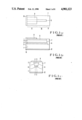
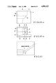
- FIGS. 1a to 1c show a buried superluminescent diode in which a non-excitation region 10 combined with an end face burying region 11 is formed.
- Reference numeral 9 denotes a current injection region; 10, a non-excitation region; and 11, an end face burying region.
- Reference numeral 13 denotes an AR coat formed on a light output surface. Since the width of an active layer 3 of the non-excitation region 10 is the same as that of the current injection region 9, light is effectively guided. Therefore, carriers are excited in the non-excitation region 10, and an absorption coefficient is reduced thereby. Therefore, in order to suppress FP mode oscillation, the length of the non-excitation region 10 must be several times longer substantially than that of the current injection region 9, i.e., must be elongated.
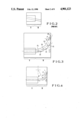
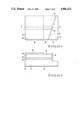
- FIG. 2 is a plan view of a buried superluminescent diode in which a non-excitation region which can solve the drawback of the diode shown in FIGS. 1a to 1c to some extent is formed.
- the feature of this diode is that the axial orientation of a cleavage end face and those of the active layers of the current injection region 9 and the non-excitation region 10 are offset from a vertical direction, and both the end faces do not easily serve as a resonator in laser oscillation.
- a suppression effect of FP mode oscillation is enhanced as the offset in the axial orientation of the active layer is larger at both the end faces and the reflected light at the end faces goes outside the waveguide.
- a light output direction is not perpendicular to the end face, it is difficult to obtain a high coupling efficiency in consideration of coupling with an optical fiber.
- a superluminescent diode comprising: a current injection portion having a current injection electrode formed adjacent to a first end face; a light-absorption portion contiguous with the current injection portion; and a waveguide continuously formed to extend from the current injection portion to the light-absorption portion, wherein the waveguide is constituted by an active layer and a member which completely buries the active layer, has a bandgap larger than that of the active layer, and is formed of a material having a small refractive index, the waveguide of the current injection portion is linearly formed to be perpendicular to the first end face, and the waveguide of the light-absorption portion has an end portion for guiding reflected light in a direction different from a propagation direction of light propagating through the waveguide.
- a measurement apparatus comprising: a light source comprising a superluminescent diode which comprises a current injection portion having a current injection electrode formed adjacent to a first end face, a light-absorption portion contiguous with the current injection portion, and a waveguide continuously formed to extend from the current injection portion to the light-absorption portion, the waveguide being constituted by an active layer and a member which completely buries the active layer, has a bandgap larger than that of the active layer, and is formed of a material having a small refractive index, the waveguide of the current injection portion being linearly formed to be perpendicular to the first end face, and the waveguide of the light-absorption portion having an end portion for guiding reflected light in a direction different from a propagation direction of light propagating through the waveguide; means for receiving light from the light source and causing backward scattered light scattered backward by an obstacle point present in the waveguide to be measured and output from the waveguide
- FIGS. 1a to 1c show a structure of conventional superluminescent diodes in which FIG. 1a is a plan view, FIG. 1b is a sectional view along a stripe direction, and FIG. 1c is a cross-sectional view;
- FIG. 2 is a plan view of another conventional diode
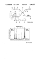
- FIGS. 3 and 4 are plan views for explaining the principle of the present invention.
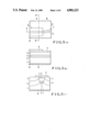
- FIGS. 5a to 5c show an embodiment of the present invention, in which FIG. 5a is a plan view, FIG. 5b is a sectional view taken along a line A--A' in FIG. 5a, and FIG. 5c is a sectional view of a light-emitting portion taken along a line B--B' in FIG. 5a;
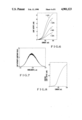
- FIG. 6 is a graph showing a temperature dependency of a light output of a superluminescent diode
- FIG. 7 is a graph showing a spectrum of the superluminescent diode
- FIG. 8 is a graph showing light coupled with a single mode fiber
- FIGS. 9a to 9c show another embodiment of the present invention, in which FIG. 9a is a plan view, FIG. 9b is a sectional view of a light guide layer, and FIG. 9c is a sectional view of a light-emitting portion;
- FIGS. 10a and 10b show still another embodiment of the present invention, in which FIG. 10a is a plan view and FIG. 10b is a side view of FIG. 10a;
- FIGS. 11a and 11b show still another embodiment of the present invention, in which FIG. 11a is a plan view an FIG. 11b is a side view of FIG. 11a;
- FIGS. 12 and 13 are plan views showing still another embodiment of the present invention.
- FIG. 14 is a diagram showing an obstacle point searching apparatus for a light waveguide utilizing the superluminescent diode of the present invention as a light source;
- FIG. 15 is a graph showing a result of obstacle point searching of an SiO 2 light waveguide by the apparatus shown in FIG. 14.
- FIG. 3 is a plan view showing the structure and principle of a superluminescent diode according to the present invention.
- the diode as a whole has a box shape.
- An active layer of a current injection region 9 is linearly formed to be perpendicular to a cleavage end face or an end face formed by polishing.
- a non-excitation region or light-absorption region 10 is formed by repeating small axial offset angles ⁇ 1 , ⁇ 2 , ⁇ 3 , . . . , ⁇ n so that almost all light emitted from the current injection region 9 can be guided with a small loss in a direction different from an extending axis of the current injection region.
- the amount of leakage of the components (1) is determined by a bending angle of the waveguide and a difference in refractive index of the active layer and a buried layer in the guide structure. As the bending angle is smaller and the refractive index difference is larger, the amount of leakage of the components (1) is small. Since the leaking light components are diffused in the buried layer and are reflected by the end face, the amount of light components which are returned to the current injection layer 9 and subjected to coupling again is small.
- the light components (2) guided to the end face are reflected by the end face, and can be escaped in a direction where the escaped light components are not coupled to the current injection region 9 at all.
- FIG. 4 is a plan view showing a case wherein the waveguide is part of a circle.
- a bent waveguide reaches a surface opposite to the output end face. If the bent waveguide reaches a side surface, the same effect as described above can be obtained.
- FIGS. 5a to 5c show an embodiment of the present invention using an InP/GaInAsP material.
- an n-type GaInAsP light guide layer ( ⁇ : 1.1 ⁇ m composition) 2
- a non-doped GaInAsP active layer ( ⁇ : 1.3 ⁇ m composition) 3
- a p-type InP cladding layer 4 and a p-type GaInAsP electrode layer ( ⁇ : 1.1 ⁇ m composition) 5 were grown on an n-type InP substrate 1 by LPE (Liquid Phase epitaxy) and VPE (Vapor Phase Epitaxy; e.g., MO-CVD (Metal Oxide-Chemical Vapor Deposition)) or MBE (Molecular Beam Epitaxy).
- LPE Liquid Phase epitaxy
- VPE Vapor Deposition
- MBE Molecular Beam Epitaxy
- an SiO 2 or SiN thin film was formed on the entire surface of the p-type GaInAsP electrode layer 5 by RF (Radio Frequency) bipolar sputterig or CVD.
- the thin film was patterned by photoetching as follows.
- the layers 5, 4, 3, and 2 were etched by a brome methanol 4% solution using the SiO 2 or SiN stripe thin layer as a mask until the substrate 1 was exposed, thereby forming an inverted mesa multilayered structure.
- a p-type InP layer 6 and an n-type InP layer 7 were buried by LPE to regulate a current in a portion removed by etching.
- An Au-Zn layer was deposited on the upper surface of the resultant wafer, and a p-type ohmic electrode 8 was formed on only the current injection region 9 by photoetching.
- an Au-Ge-Ni layer was deposited on the substrate to form an n-type ohmic electrode 12 on the entire surface.
- the structures of the layers of the resultant element in the state of FIG. 5 are as follows, and the respective crystalline layers match with an InP lattice constant:
- An nti-reflecting coat 13 comprising a multilayered film of SiO 2 and TiO 2 was formed on the light output end face so as to obtain a reflectivity of 0.5% or less with respect to light having a wavelength of 1.3 ⁇ m.
- the element was divided into uniform pellets having a total length of 600 ⁇ m and a width of 400 ⁇ m, each pellet was mounted on a heat sink by AuSn soldering, and a current and light output characteristics with respect to light having a wavelength of 1.3 ⁇ m were measured. As a result, a light output was increased without causing oscillation along with current injection in a 25° C. continuous operation, and an incoherent light output of 12 mW could be obtained at 200 mA.
- the total element length could be shortened to 1/4 or less of that of the conventional element, and FP mode oscillation could be sufficiently suppressed.
- FIG. 6 shows a temperature dependency of the superluminescent diode of the structure shown in FIG. 5.
- a light output of 3 mW is available at a high temperature of 50° C. and a current of 200 mA.
- FIG. 7 shows a spectrum of the superluminescent diode shown in FIG. 5.
- FP mode oscillation can be sufficiently suppressed at a high output of 10 mW.
- a coherence length is as short as about 30 ⁇ m at an output of 10 mW.
- a far field pattern determining a radiation angle of light was measured, it was as narrow as 52° in a direction perpendicular to the active layer and 48° in a direction parallel to the active layer. Thus, sharp directivity could be obtained.
- FIG. 8 shows results of a light input test by lens coupling to a single mode fiber having a core diameter of 10 ⁇ m.
- a high light input of 800 ⁇ W could be obtained at 25° C. and 150 mA.
- this embodiment employs the n-type InP substrate.
- a p-type InP substrate is used.
- n- and p-type regions are replaced.
- a BH (Buried Hetero) type or buried type superluminescent diode has been exemplified.
- the same effect as described above can be obtained if the present invention is applied to a DCPBH (Double Channel Planar Buried Heterostructure laser) or VSB (V-grooved Substrate Buried-Heterostructure laser) type diode.
- DCPBH Double Channel Planar Buried Heterostructure laser
- VSB V-grooved Substrate Buried-Heterostructure laser
- the lenth of the electrode 8 of the current injection portion is 400 ⁇ m.
- a superluminescent diode having a wide spectrum could be realized.
- FIGS. 9a to 9c show another embodiment of the present invention using a GaAs/AlGaAs material.
- various growth techniques are available as in Embodiment 1.
- a 0.5- ⁇ m thick n-type GaAs buffer layer 15 in a first growth, a 0.5- ⁇ m thick n-type GaAs buffer layer 15, a 1- ⁇ m thick n-type Al 0 .35 Ga 0 .65 As cladding layer 16, a 0.5- ⁇ m thick non-doped Al 0 .05 Ga 0 .95 As active layer 17, a 0.10- ⁇ m thick p-type Al 0 .20 Ga 0 .80 As light guide layer 18, a 2- ⁇ m thick p-type Al 0 .35 Ga 0 .65 As cladding layer 19, and a 0.5- ⁇ m thick p-type GaAs electrode layer 20 were sequentially grown on an n-type GaAs substrate 14.
- an inverted mesa multilayered structure was formed following the same procedures as in Embodiment 1 to perform burying growth in the subsequent process.
- a p-type Al 0 .35 Ga 0 .65 As layer 21 and an n-type Al 0 .35 Ga 0 .65 As layer 22 were buried by LPE in a portion removed by etching so as to obtain current regulating and optical confinement effects.
- the structures of the respectively layers of the resultant element in FIGS. 9a to 9c are as follows, and the respectively crystalline layers match with a GaAs lattice constant:
- the resultant wafer was subjected to formation of a p-type ohmic electrode, substrate polishing, and formation of an n-type ohmic electrode, and thereafter was mounted on a heat sink.
- Current-light output characteristics and a light-emission spectrum of the wafer were measured.
- a light output was increased along with an increase in injected current, and a light output of 18 mW could be obtained at 150 mA.
- a element having an AR coat on its light extraction surface could provide a light output of twice to three times, and recorded 38 mW at 150 mA.
- As for the light-emission spectrum an incoherent light output having a half-width of 200 ⁇ could be obtained while suppressing FP mode oscillation as in Embodiment 1, and the light-emission center wavelength was 0.83 ⁇ m.
- the GaInAsP element having a wavelength of 1.3 ⁇ m and the GaAs/GaAlAs element having a wavelength of 0.83 ⁇ m have been exemplified.
- the present invention can be applied to incoherent light-emitting elements using other wavelength ranges and different semiconductors.
- FIGS. 10a and 10b show still another embodiment of the present invention using an InP/GaInAsP material.
- an n-type GaInAsP light guide layer ( ⁇ : 1.1 ⁇ m composition) 32, a non-doped GaInAsP active layer ( ⁇ : 1.3 ⁇ m composition) 33, a p-type InP cladding layer 34, and a p-type GaInAsP electrode layer ( ⁇ : 1.1 ⁇ m composition) 35 were grown on an n-type InP substrate 31 by LPE and VPE or MBE.
- An SiO 2 or SiN thin film was formed on the entire surface of the p-type GaInAsP electrode layer 35 by RF bipolar sputter or CVD. Thereafter, in order to bury the active layer, the thin film was linearly patterned by photoetching in a stripe shape along a ⁇ 110> direction to have a width of 4 to 5 ⁇ m. Thereafter, the layers 35, 34, 33, and 32 were etched to expose the substrate 31 by a brome methanol 4% solution using the SiO 2 or SiN stripe thin film as a mask, thereby forming an inverted mesa multilayered structure.
- a p-type InP layer 36 and an n-type InP layer 37 were buried by LPE in a portion removed by etching to obtain a current regulating effect.
- An Au-Zn layer was deposited on the upper surface of the resultant wafer, and an electrode pattern on one end face was formed by photoetching to have an angle with a light-radiation direction of 20° so that a p-type ohmic electrode 38 was formed on only the current injection region 9.
- the substrate 31 was polished to have a total thickness of about 80 ⁇ m, and thereafter, an Au-Ge-Ni layer was deposited thereon to form an n-type ohmic electrode 42 on the entire surface.
- the structures of the respective layers of the resultant element in FIGS. 10a and 10b are as follows, and the respectively crystalline layers match with an InP lattice constant:
- an SiO 2 film was formed on the entire surface on the side of the p-type electrode, and was patterned by photoetching to be left on only the current injection region 9.
- the resultant structure was etched using a Br-based gas by an RIE (Reactive Ion Etching) apparatus using SiO 2 film pattern as a mask to etch a region 44 excluding the region 9 until the substrate was exposed, thus forming an FP mode oscillation suppression end face 45 serving as a light-absorption portion.
- RIE Reactive Ion Etching
- An anti-reflecting coat comprising a multilayered film of SiO 2 and TiO 2 was formed on the light output end face to obtain a reflectivity of 0.5% or less with respect to light having a wavelength of 1.3 ⁇ m.
- the resultant element was divided into uniform pellets having a total length of 500 ⁇ m and a width of 400 ⁇ m, and a 400- ⁇ m wide current injection region 9. Each pellet was monted on a heat sink by AuSn soldering, and its current and light output characteristics at a wavelength of 1.3 ⁇ m were measured. As a result, a light output was increased without causing oscillation along with current injection in a 25° C. continuous operation, and an incoherent light output of 12 mW could be obtained at 200 mA.
- a light output of 1 mW could be obtained at an injection current of 175 mA upon coupling with an SLM (single mode) fiber having a core diameter of 10 ⁇ m through a lens.
- a structure wherein a mesa structure including an active portion is buried with an organic material such as polyimide or low-melting point glass is available as well as a structure wherein the mesa structure is buried with a group III-V single crystalline epitaxial layer.
- an organic material such as polyimide or low-melting point glass
- a structure wherein the mesa structure is buried with a group III-V single crystalline epitaxial layer since a difference in refractive index between the active portion and a buried portion is large, a loss is small even if an angle ⁇ of the bent guide portion or the bending angle of the waveguide portion is large. Thus, light can be effectively guided to the end face by the non-excitation portion and can be reflected at a large incident angle so as not to be returned to the active portion.
- a structure wherein the active layer of the non-excitation portion is tapered, and the tapered end is buried in the end face is available.
- a leading end E of a waveguide of the light-absorption portion 10 is separated from all the end faces.
- most part of the waveguide of the light-absorption portion 10 is linearly formed, and a predetermined bending angle P is formed at a connecting portion with an excitation portion, e.g., the current injection portion 9 so as to offset the optical axes of the current injection portion 9 and the light-absorption portion 10.
- a non-current injection portion for guiding light in a direction different from an extending axis of a current injection portion is formed contiguous with the linear current injection portion, return of light from the end face to a light-emitting portion can be sufficiently prevented, and hence, FP mode oscillation can be sufficiently suppressed.
- the suppression effect of FP mode oscillation has two characteristic features, that is, a light-absorption effect at the non-current injection portion and guiding of light in a direction quite different from the extending axis direction of the light-emitting portion. Since FP mode oscillation can be efficiently suppressed, the element length can be reduced.
- the active layer or the waveguide has an MQW (Multi Quantum Well) structure, a wave length shift at an absorption end upon current injection immediately occurs. Thus, the effect of oblique reflection at the end face is conspicuous.
- MQW Multi Quantum Well
- the superluminescent diode of the present invention can be applied as a light source for a variety of optical measurement equipment.
- FIG. 14 shows the light waveguide obstacle searching apparatus.
- a light source having a large spectrum width is used, and light emitted from the light source is guided to become incident on a light waveguide to be measured.
- Backward scattered light which is scattered backward at obstacle points scattered in the light waveguide and propagates toward an incident direction is caused to interfere with reference light to provide a delay time or an optical path difference to the backward scattered light and the reference light.
- An interfered portion with respect to each delay time is measured to detect power of light scattered in the light waveguide, thus obtaining the positions of the obstacle points.
- reference numeral 133 denotes a focusing lens; 134, a fiber type photocoupler; 135, a cylindrical electrostrictive oscillator; 136, a total reflection mirror; 137, a collimator lens; and 138, a total reflection mirror.
- a light-emitting diode 123 is one described in the above embodiments, and light emitted from the diode is collimated to parallel light by a collimatorlens 124. Thereafter, the parallel light is incident on the fiber type photocoupler 134 through the fcusing lens 133.
- the fiber type photocoupler 134 can distribute light incident from one branch portion C 1 in two directions, i.e., toward branch portions C 2 and C 3 .
- An output end of the branch portion C 2 of the photocoupler 134 is arranged to excite a propagation mode of a light waveguide 128 to be measured. Light incident on the branch portion C 2 is incident on the light waveguide 128 from the output end of the fiber of the branch portion C 2 .
- Backward scattered light generated in this light waveguide is incident again on the fiber of the branch portion C 2 , and is output from the fiber of a branch portion C 4 through the branch portion C 4 .
- Light incident from the branch portion C 1 and distributed to the branch portion C 3 is totally reflected by the total reflection mirror 136 arranged at the fiber output end of the branch portion C 3 , and propagates toward the branch portion C 3 again.
- This light is mixed with the backward scattered light scattered in the light waveguide 128 and returned through the branch portion C 2 .
- the mixed light is output through the branch portion C 4 , and is collimated to parallel light by the collimator lens 137. Thereafter, the parallel light is split into two directions by a beam splitter 125.
- the light passing through the beam splitter 125 is reflected by a total reflection mirror 126 and is then reflected by the beam splitter 125.
- the reflected light is mixed with light which is reflected by the beam splitter 125 and is then reflected by the total reflection mirror 138 to be returned to the beam splitter 125.
- the mixed light is incident on a photodetector 129.
- the fiber of the branch portion C 2 of the fiber type photocoupler is wound around the cylindrical electrostrictive oscillator 135.
- the electrostrictive oscillator 135 is AC-driven at a resonance frequency of 20 kHz, and light propagating through the fiber of the branch portion C 3 is phase-modulated. Therefore, the backward scattered light propagating through the branch portion C 2 is also phase-modulated.
- the phase-modulated backward scattered light is caused to interfere with reference light which propagates through the branch portion C 3 , is reflected by the total reflection mirror 136, and propagates through the branch portion C 3 again, the amplitude of an interference intensity is oscillated at 20 kHz.
- the 20-kHz component is detected by a selection level meter 131.
Landscapes
- Physics & Mathematics (AREA)
- Optics & Photonics (AREA)
- General Physics & Mathematics (AREA)
- Chemical & Material Sciences (AREA)
- Analytical Chemistry (AREA)
- Condensed Matter Physics & Semiconductors (AREA)
- Electromagnetism (AREA)
- Led Devices (AREA)
Abstract
Description
Claims (8)
Applications Claiming Priority (6)
| Application Number | Priority Date | Filing Date | Title |
|---|---|---|---|
| JP30329687 | 1987-12-02 | ||
| JP20602488 | 1988-08-19 | ||
| JP63-206024 | 1988-08-19 | ||
| JP62-303296 | 1988-08-19 | ||
| JP63-249627 | 1988-10-03 | ||
| JP24962788A JPH0682863B2 (en) | 1987-12-02 | 1988-10-03 | Light emitting diode |
Publications (1)
| Publication Number | Publication Date |
|---|---|
| US4901123A true US4901123A (en) | 1990-02-13 |
Family
ID=27328575
Family Applications (1)
| Application Number | Title | Priority Date | Filing Date |
|---|---|---|---|
| US07/277,088 Expired - Lifetime US4901123A (en) | 1987-12-02 | 1988-11-28 | Superluminescent diode |
Country Status (4)
| Country | Link |
|---|---|
| US (1) | US4901123A (en) |
| EP (1) | EP0318947B1 (en) |
| JP (1) | JPH0682863B2 (en) |
| DE (1) | DE3887840T2 (en) |
Cited By (24)
| Publication number | Priority date | Publication date | Assignee | Title |
|---|---|---|---|---|
| US5008889A (en) * | 1989-11-06 | 1991-04-16 | Wilson Keith E | High-accuracy wavelength stabilization of angled-stripe super luminescent laser diode sources |
| US5034955A (en) * | 1988-11-30 | 1991-07-23 | Oki Electric Industry Co., Ltd. | Superluminescent diode |
| US5093884A (en) * | 1990-06-13 | 1992-03-03 | Commissariat A L'energie Atomique | Integrated monomode spatial optical filter and its method of embodiment |
| US5223722A (en) * | 1991-03-26 | 1993-06-29 | Mitsubishi Denki Kabushiki Kaisha | Superluminescent diode |
| US5329134A (en) * | 1992-01-10 | 1994-07-12 | International Business Machines Corporation | Superluminescent diode having a quantum well and cavity length dependent threshold current |
| US5357124A (en) * | 1992-07-22 | 1994-10-18 | Mitsubishi Precision Co. Ltd | Superluminescent diode with stripe shaped doped region |
| US5396511A (en) * | 1991-11-07 | 1995-03-07 | Hitachi, Ltd. | Semiconductor laser apparatus with curved waveguide |
| US5737352A (en) * | 1995-11-08 | 1998-04-07 | U.S. Philips Corporation | Semiconductor diode laser, in particular a laser amplifier, and method of manufacturing this laser |
| US6091755A (en) * | 1997-11-21 | 2000-07-18 | Sdl, Inc. | Optically amplifying semiconductor diodes with curved waveguides for external cavities |
| US6184542B1 (en) | 1998-06-16 | 2001-02-06 | Princeton Lightwave | Superluminescent diode and optical amplifier with extended bandwidth |
| US6262415B1 (en) | 1999-07-29 | 2001-07-17 | Litton Systems, Inc. | Orientation sensor system with high precision optical interrogation and dense multiplexing |
| US20020003825A1 (en) * | 2000-07-07 | 2002-01-10 | Per Granestrand | Optical device and fabrication thereof |
| US20030026573A1 (en) * | 2001-08-01 | 2003-02-06 | Matsushita Electric Industrial Co., Ltd. | Optical waveguide device and coherent light source and optical apparatus using the same |
| US6593602B2 (en) * | 2000-08-30 | 2003-07-15 | Stanley Electric Co., Ltd. | Edge emission type semiconductor device for emitting super luminescent light, its manufacture and spatial optical communication device |
| US20040126063A1 (en) * | 2000-02-25 | 2004-07-01 | Alphonse Gerard A | Multi-pass, arcuate bent waveguide, high power super luminescent diode |
| US20040238828A1 (en) * | 2003-03-14 | 2004-12-02 | Sumitomo Electric Industries, Ltd. | Semiconductor optical integrated device |
| US6839376B2 (en) * | 2000-12-07 | 2005-01-04 | Fuji Photo Film Co., Ltd. | Laser light source |
| US20100238962A1 (en) * | 2009-03-23 | 2010-09-23 | Electronics And Telecommunications Research Institute | External cavity laser light source |
| US20110090557A1 (en) * | 2009-10-15 | 2011-04-21 | Citizen Holdings Co., Ltd. | Laser source |
| US20110103418A1 (en) * | 2009-11-03 | 2011-05-05 | The Regents Of The University Of California | Superluminescent diodes by crystallographic etching |
| CN104485403A (en) * | 2014-12-31 | 2015-04-01 | 中国科学院半导体研究所 | Curved waveguide quantum dot super-luminescent diode with gradually-varied curvature and manufacturing method thereof |
| US11125689B2 (en) * | 2018-07-13 | 2021-09-21 | The Government Of The United States Of America, As Represented By The Secretary Of The Navy | Highly stable semiconductor lasers and sensors for III-V and silicon photonic integrated circuits |
| CN116093238A (en) * | 2023-02-23 | 2023-05-09 | 河南仕佳光子科技股份有限公司 | Super-radiation light-emitting diode |
| US20230283046A1 (en) * | 2020-08-20 | 2023-09-07 | Nippon Telegraph And Telephone Corporation | Semiconductor Chip and Optical Module |
Families Citing this family (10)
| Publication number | Priority date | Publication date | Assignee | Title |
|---|---|---|---|---|
| US5252839A (en) * | 1992-06-10 | 1993-10-12 | Hewlett-Packard Company | Superluminescent light-emitting diode with reverse biased absorber |
| AU4887596A (en) * | 1995-03-07 | 1996-09-23 | British Telecommunications Public Limited Company | A laser |
| US6034380A (en) * | 1997-10-07 | 2000-03-07 | Sarnoff Corporation | Electroluminescent diode with mode expander |
| GB0215669D0 (en) * | 2002-07-05 | 2002-08-14 | Denselight Semiconductors Pte | Superluminescent diode |
| US20040061122A1 (en) * | 2002-09-27 | 2004-04-01 | Gerard Alphonse | Light emitting device with low back facet reflections |
| WO2012150647A1 (en) * | 2011-05-02 | 2012-11-08 | パナソニック株式会社 | Super-luminescent diode |
| JP5403305B2 (en) * | 2013-01-23 | 2014-01-29 | セイコーエプソン株式会社 | Light emitting device |
| PL224641B1 (en) * | 2014-06-03 | 2017-01-31 | Wrocławskie Centrum Badań Eit + Spółka Z Ograniczoną | AlInGaN-based superluminescent diode |
| PL228006B1 (en) | 2015-09-23 | 2018-02-28 | Inst Wysokich Ciśnień Polskiej Akademii Nauk | AlInGaN-based superluminescent diode |
| EP3893326B1 (en) * | 2020-04-06 | 2026-02-18 | Nokia Technologies Oy | Apparatus comprising a waveguide for radio frequency signals |
Citations (4)
| Publication number | Priority date | Publication date | Assignee | Title |
|---|---|---|---|---|
| US4634928A (en) * | 1985-04-19 | 1987-01-06 | Trw Inc. | Superluminescent light-emitting diode and related method |
| US4718070A (en) * | 1985-01-22 | 1988-01-05 | Massachusetts Institute Of Technology | Surface emitting diode laser |
| US4730331A (en) * | 1985-04-03 | 1988-03-08 | Xerox Corporation | Superluminescent LED source |
| US4799229A (en) * | 1986-05-15 | 1989-01-17 | Canon Kabushiki Kaisha | Semiconductor laser array |
Family Cites Families (1)
| Publication number | Priority date | Publication date | Assignee | Title |
|---|---|---|---|---|
| JPS5743485A (en) * | 1980-08-13 | 1982-03-11 | Agency Of Ind Science & Technol | Semiconductor ring laser device |
-
1988
- 1988-10-03 JP JP24962788A patent/JPH0682863B2/en not_active Expired - Lifetime
- 1988-11-28 US US07/277,088 patent/US4901123A/en not_active Expired - Lifetime
- 1988-11-30 DE DE3887840T patent/DE3887840T2/en not_active Expired - Lifetime
- 1988-11-30 EP EP88119963A patent/EP0318947B1/en not_active Expired - Lifetime
Patent Citations (4)
| Publication number | Priority date | Publication date | Assignee | Title |
|---|---|---|---|---|
| US4718070A (en) * | 1985-01-22 | 1988-01-05 | Massachusetts Institute Of Technology | Surface emitting diode laser |
| US4730331A (en) * | 1985-04-03 | 1988-03-08 | Xerox Corporation | Superluminescent LED source |
| US4634928A (en) * | 1985-04-19 | 1987-01-06 | Trw Inc. | Superluminescent light-emitting diode and related method |
| US4799229A (en) * | 1986-05-15 | 1989-01-17 | Canon Kabushiki Kaisha | Semiconductor laser array |
Non-Patent Citations (6)
| Title |
|---|
| OFS 88 FDD 2 1, pp. 451 454 (1988), Jan.) N. S. K. Kwong et al. * |
| OFS'88 FDD 2-1, pp. 451-454 (1988), Jan.) N. S. K. Kwong et al. |
| OQE87 39, pp. 71 75, 1987 by Tanioka et al. * |
| OQE87-39, pp. 71-75, 1987 by Tanioka et al. |
| SPIE vol. 719, Fiber Optic Gyros: 10th Anniversary Conference 1986 pp. 208 215. * |
| SPIE vol. 719, Fiber Optic Gyros: 10th Anniversary Conference 1986 pp. 208-215. |
Cited By (37)
| Publication number | Priority date | Publication date | Assignee | Title |
|---|---|---|---|---|
| US5034955A (en) * | 1988-11-30 | 1991-07-23 | Oki Electric Industry Co., Ltd. | Superluminescent diode |
| US5008889A (en) * | 1989-11-06 | 1991-04-16 | Wilson Keith E | High-accuracy wavelength stabilization of angled-stripe super luminescent laser diode sources |
| US5093884A (en) * | 1990-06-13 | 1992-03-03 | Commissariat A L'energie Atomique | Integrated monomode spatial optical filter and its method of embodiment |
| US5223722A (en) * | 1991-03-26 | 1993-06-29 | Mitsubishi Denki Kabushiki Kaisha | Superluminescent diode |
| US5396511A (en) * | 1991-11-07 | 1995-03-07 | Hitachi, Ltd. | Semiconductor laser apparatus with curved waveguide |
| US5329134A (en) * | 1992-01-10 | 1994-07-12 | International Business Machines Corporation | Superluminescent diode having a quantum well and cavity length dependent threshold current |
| US5556795A (en) * | 1992-01-10 | 1996-09-17 | International Business Machines Corporation | Quantum well superluminescent diode |
| US5357124A (en) * | 1992-07-22 | 1994-10-18 | Mitsubishi Precision Co. Ltd | Superluminescent diode with stripe shaped doped region |
| US5737352A (en) * | 1995-11-08 | 1998-04-07 | U.S. Philips Corporation | Semiconductor diode laser, in particular a laser amplifier, and method of manufacturing this laser |
| US6091755A (en) * | 1997-11-21 | 2000-07-18 | Sdl, Inc. | Optically amplifying semiconductor diodes with curved waveguides for external cavities |
| US6118802A (en) * | 1997-11-21 | 2000-09-12 | Sdl, Inc. | Optically amplifying semiconductor diodes with curved waveguides for external cavities |
| US6118803A (en) * | 1997-11-21 | 2000-09-12 | Sdl, Inc. | Optically amplifying semiconductor diodes with curved waveguides for external cavities |
| US6184542B1 (en) | 1998-06-16 | 2001-02-06 | Princeton Lightwave | Superluminescent diode and optical amplifier with extended bandwidth |
| US6262415B1 (en) | 1999-07-29 | 2001-07-17 | Litton Systems, Inc. | Orientation sensor system with high precision optical interrogation and dense multiplexing |
| US20040126063A1 (en) * | 2000-02-25 | 2004-07-01 | Alphonse Gerard A | Multi-pass, arcuate bent waveguide, high power super luminescent diode |
| US6937780B2 (en) | 2000-02-25 | 2005-08-30 | Trumpf Photonics, Inc. | Multi-pass, arcuate bent waveguide, high power super luminescent diode |
| US20020003825A1 (en) * | 2000-07-07 | 2002-01-10 | Per Granestrand | Optical device and fabrication thereof |
| US6914924B2 (en) | 2000-07-07 | 2005-07-05 | Telefonaktiebolaget Lm Ericsson (Publ) | Optical device and fabrication thereof |
| WO2002005398A1 (en) * | 2000-07-07 | 2002-01-17 | Telefonaktiebolaget Lm Ericsson | Optical device and fabrication thereof |
| US6593602B2 (en) * | 2000-08-30 | 2003-07-15 | Stanley Electric Co., Ltd. | Edge emission type semiconductor device for emitting super luminescent light, its manufacture and spatial optical communication device |
| US6839376B2 (en) * | 2000-12-07 | 2005-01-04 | Fuji Photo Film Co., Ltd. | Laser light source |
| US20030026573A1 (en) * | 2001-08-01 | 2003-02-06 | Matsushita Electric Industrial Co., Ltd. | Optical waveguide device and coherent light source and optical apparatus using the same |
| US6785457B2 (en) * | 2001-08-01 | 2004-08-31 | Matsushita Electric Industrial Co., Ltd. | Optical waveguide device and coherent light source and optical apparatus using the same |
| US20040238828A1 (en) * | 2003-03-14 | 2004-12-02 | Sumitomo Electric Industries, Ltd. | Semiconductor optical integrated device |
| US8107508B2 (en) * | 2009-03-23 | 2012-01-31 | Electronics And Telecommunications Research Institute | External cavity laser light source |
| US20100238962A1 (en) * | 2009-03-23 | 2010-09-23 | Electronics And Telecommunications Research Institute | External cavity laser light source |
| US20110090557A1 (en) * | 2009-10-15 | 2011-04-21 | Citizen Holdings Co., Ltd. | Laser source |
| US8451530B2 (en) | 2009-10-15 | 2013-05-28 | Citizen Holdings Co., Ltd. | Laser source |
| US20110103418A1 (en) * | 2009-11-03 | 2011-05-05 | The Regents Of The University Of California | Superluminescent diodes by crystallographic etching |
| CN104485403A (en) * | 2014-12-31 | 2015-04-01 | 中国科学院半导体研究所 | Curved waveguide quantum dot super-luminescent diode with gradually-varied curvature and manufacturing method thereof |
| US11125689B2 (en) * | 2018-07-13 | 2021-09-21 | The Government Of The United States Of America, As Represented By The Secretary Of The Navy | Highly stable semiconductor lasers and sensors for III-V and silicon photonic integrated circuits |
| US20210389242A1 (en) * | 2018-07-13 | 2021-12-16 | The Government Of The United States Of America, As Represented By The Secretary Of The Navy | Highly Stable Semiconductor Lasers and Sensors for III-V and Silicon Photonic Integrated Circuits |
| US20210404957A1 (en) * | 2018-07-13 | 2021-12-30 | The Government Of The United States Of America, As Represented By The Secretary Of The Navy | Highly Stable Semiconductor Lasers and Sensors for III-V and Silicon Photonic Integrated Circuits |
| US11709135B2 (en) * | 2018-07-13 | 2023-07-25 | The Government of the United States of America, as represented by the Secretary of the Naw | Highly stable semiconductor lasers and sensors for III-V and silicon photonic integrated circuits |
| US11761892B2 (en) * | 2018-07-13 | 2023-09-19 | The Government Of The United States Of America, As Represented By The Secretary Of The Navy | Highly stable semiconductor lasers and sensors for III-V and silicon photonic integrated circuits |
| US20230283046A1 (en) * | 2020-08-20 | 2023-09-07 | Nippon Telegraph And Telephone Corporation | Semiconductor Chip and Optical Module |
| CN116093238A (en) * | 2023-02-23 | 2023-05-09 | 河南仕佳光子科技股份有限公司 | Super-radiation light-emitting diode |
Also Published As
| Publication number | Publication date |
|---|---|
| DE3887840D1 (en) | 1994-03-24 |
| EP0318947B1 (en) | 1994-02-16 |
| DE3887840T2 (en) | 1994-09-22 |
| JPH02146778A (en) | 1990-06-05 |
| EP0318947A2 (en) | 1989-06-07 |
| JPH0682863B2 (en) | 1994-10-19 |
| EP0318947A3 (en) | 1990-06-13 |
Similar Documents
| Publication | Publication Date | Title |
|---|---|---|
| EP0318947B1 (en) | Superluminescent diode | |
| US4821277A (en) | Super-luminescent diode | |
| US4063189A (en) | Leaky wave diode laser | |
| US4894835A (en) | Surface emitting type semiconductor laser | |
| US4958355A (en) | High performance angled stripe superluminescent diode | |
| JPH0277185A (en) | Grating coupled type surface emitting laser element and modulation thereof | |
| US6593602B2 (en) | Edge emission type semiconductor device for emitting super luminescent light, its manufacture and spatial optical communication device | |
| US4821276A (en) | Super-luminescent diode | |
| US4615032A (en) | Self-aligned rib-waveguide high power laser | |
| US4045749A (en) | Corrugation coupled twin guide laser | |
| JPS59144193A (en) | Semiconductor laser | |
| JPH0497206A (en) | Semiconductor optical element | |
| US4679200A (en) | Semiconductor laser | |
| JP2778985B2 (en) | Super luminescent diode | |
| US4718069A (en) | Semiconductor laser array with single lobed output | |
| JP2022501815A (en) | Gain-guided semiconductor laser and its manufacturing method | |
| JPS6140159B2 (en) | ||
| KR100576299B1 (en) | Semiconductor laser and element for optical communication | |
| JP3685925B2 (en) | Super luminescent diode | |
| JPH11284223A (en) | Superluminascent diode | |
| JPH055391B2 (en) | ||
| JP2759275B2 (en) | Light emitting diode and method of manufacturing the same | |
| US4847847A (en) | Semiconductor laser array | |
| JP3208860B2 (en) | Semiconductor laser device | |
| JP2011192856A (en) | Semiconductor light-emitting element and optical pulse tester using the same |
Legal Events
| Date | Code | Title | Description |
|---|---|---|---|
| AS | Assignment |
Owner name: NIPPON TELEGRAPH AND TELEPHONE CORPORATION, 1-6, U Free format text: ASSIGNMENT OF ASSIGNORS INTEREST.;ASSIGNORS:NOGUCHI, YOSHIO;NAGAI, HARUO;TAKADA, KAZUMASA;AND OTHERS;REEL/FRAME:004988/0040 Effective date: 19881118 Owner name: NIPPON TELEGRAPH AND TELEPHONE CORPORATION, A CORP Free format text: ASSIGNMENT OF ASSIGNORS INTEREST;ASSIGNORS:NOGUCHI, YOSHIO;NAGAI, HARUO;TAKADA, KAZUMASA;AND OTHERS;REEL/FRAME:004988/0040 Effective date: 19881118 |
|
| STCF | Information on status: patent grant |
Free format text: PATENTED CASE |
|
| FEPP | Fee payment procedure |
Free format text: PAYOR NUMBER ASSIGNED (ORIGINAL EVENT CODE: ASPN); ENTITY STATUS OF PATENT OWNER: LARGE ENTITY |
|
| FPAY | Fee payment |
Year of fee payment: 4 |
|
| AS | Assignment |
Owner name: NIPPON TELGRAPH AND TELEPHONE CORPORATION, JAPAN Free format text: CHANGE OF ADDRESS;ASSIGNOR:NIPPON TELEGRAPH AND TELEPHONE CORPORATION;REEL/FRAME:008067/0690 Effective date: 19960322 |
|
| FPAY | Fee payment |
Year of fee payment: 8 |
|
| FPAY | Fee payment |
Year of fee payment: 12 |