US4878192A - Arithmetic processor and divider using redundant signed digit arithmetic - Google Patents
Arithmetic processor and divider using redundant signed digit arithmetic Download PDFInfo
- Publication number
- US4878192A US4878192A US07/070,565 US7056587A US4878192A US 4878192 A US4878192 A US 4878192A US 7056587 A US7056587 A US 7056587A US 4878192 A US4878192 A US 4878192A
- Authority
- US
- United States
- Prior art keywords
- digit
- bit
- signal
- bit signal
- arithmetic
- Prior art date
- Legal status (The legal status is an assumption and is not a legal conclusion. Google has not performed a legal analysis and makes no representation as to the accuracy of the status listed.)
- Expired - Lifetime
Links
Images
Classifications
-
- G—PHYSICS
- G06—COMPUTING OR CALCULATING; COUNTING
- G06F—ELECTRIC DIGITAL DATA PROCESSING
- G06F7/00—Methods or arrangements for processing data by operating upon the order or content of the data handled
- G06F7/38—Methods or arrangements for performing computations using exclusively denominational number representation, e.g. using binary, ternary, decimal representation
- G06F7/48—Methods or arrangements for performing computations using exclusively denominational number representation, e.g. using binary, ternary, decimal representation using non-contact-making devices, e.g. tube, solid state device; using unspecified devices
- G06F7/4824—Methods or arrangements for performing computations using exclusively denominational number representation, e.g. using binary, ternary, decimal representation using non-contact-making devices, e.g. tube, solid state device; using unspecified devices using signed-digit representation
-
- G—PHYSICS
- G06—COMPUTING OR CALCULATING; COUNTING
- G06F—ELECTRIC DIGITAL DATA PROCESSING
- G06F7/00—Methods or arrangements for processing data by operating upon the order or content of the data handled
- G06F7/38—Methods or arrangements for performing computations using exclusively denominational number representation, e.g. using binary, ternary, decimal representation
- G06F7/48—Methods or arrangements for performing computations using exclusively denominational number representation, e.g. using binary, ternary, decimal representation using non-contact-making devices, e.g. tube, solid state device; using unspecified devices
- G06F7/52—Multiplying; Dividing
- G06F7/535—Dividing only
- G06F7/537—Reduction of the number of iteration steps or stages, e.g. using the Sweeny-Robertson-Tocher [SRT] algorithm
- G06F7/5375—Non restoring calculation, where each digit is either negative, zero or positive, e.g. SRT
Definitions
- the present invention relates to an arithmetic processor capable of high-speed arithmetic operation and to an arithmetic addition/subtraction unit therefor, and, more particularly, to a high-speed arithmetic processor which has a cellular array structure including a number of such arithmetic addition/subtraction units which may be compactly fabricated on an LSI chip.
- a high speed adder, multiplier and divider are respectively discussed in Trans. of IECE Japan, No.2, 1986, pp.187; Trans. of IECE Japan, Vol.J66-D, No.6, 1983, pp.683 to 690; and Trans. of IECE Japan, Vol.J67-D, No.4, 1984, pp.450 to 457.
- Those arithmetic units execute multiplication or division by means of combinational circuitry using the redundant binary expression (a kind of signed digit expression) in which each digit is represented by a set of elements ⁇ -1, 0, 1 ⁇ .
- a prior art divider of the shift, subtract restore type uses the redundant binary expression and is implemented by ECL (emitter-coupled-logic) circuitry. While that prior art divider has faster arithmetic processing speeds than other types of conventional dividers, no consideration has been given to factors which are important for fabricating such a divider commercially, such as a reduction in the number and size of transistors and use of other types of circuitry, e.g., CMOS.
- Dividers in wide use today are sequential circuits each having a subtracter (adder) and a shifter.
- adder subtracter
- shifter shifter
- large-size computers having high-speed multipliers often employ multiplication-type division in which division is performed by repetition of multiplication.
- implementation of such multiplication-type division by combinational circuitry requires large numbers of hardware elements, and is therefore impractical.
- the OR circuit is implemented by elements formed in two stages, that is, a NOR gate and an inverter, and the number of stages or gates required in the arithmetic circuit increases correspondingly, resulting in an increase in operation time.
- an arithmetic processor and an addition/subtraction unit therefor are provided, the arithmetic processor comprising a plurality of the addition/subtraction units arranged in parallel, each unit being capable of carrying out addition (or subtraction) with respect to respective digits of two operands.
- An addition/subtraction unit comprises a first circuit and a second circuit coupled to receive binary signals each representing a respective digit of the operands. At least a first of the two binary signals is a 2-bit signal representing a signed digit expression, one bit of which (“the sign bit”) represents the sign of one of the digits of the operands and the other bit of which (“the magnitude bit”) represents the magnitude of that one digit of the operands.
- the first circuit provides a bindary signal representing an intermediate carry (or borrow) and the second circuit provides a binary signal representing an intermediate sum (or difference) from the two binary signals representing the digits of the operands.
- the addition/subtraction unit further comprises a third circuit which is coupled to receive the intermediate sum (or difference) binary signal output from the second circuit and a binary signal representing an intermediate carry (or borrow) from a next-lower-order digit, and outputs a 2-bit binary signal representing an addend (or subtrahend).
- That 2-bit signal output by the third circuit represents a signed digit expression, one bit, i.e., the sign bit, of which represents the sign of the addend (or subtrahend) and the other bit, i.e., the magnitude bit, of which represents the magnitude of the addend (or subtrahend).
- the arithmetic processor also includes first means for receiving the first binary signal and a 1-bit control signal, and for providing an output signal which is either the same as the first binary signal or is inverted in sign with respect to the first binary signal depending on the 1-bit control signal.
- the first means comprises an exclusive logical OR circuit having inputs coupled to receive the sign bit of the 2-bit first binary signal, and the 1-bit control signal, and having an output on which one bit (the sign bit) of the first means output signal is provided.
- the first means output signal is a 2-bit signal, the second bit of which is the magnitude bit of the first binary signal.
- the arithmetic processor includes second means for receiving a second of the two binary signals representing a respective digit of the operands and a 1-bit control signal, and for selectively converting the second binary signal to an output signal which is a logical "0" in response to the 1-bit control signal.
- the second means comprises a logical NOR circuit having inputs which receive the second binary signal and the control signal, and an output on which the second means output signal is provided as a logical "0" when the control signal is a logical "1".
- the second circuit comprises an exclusive logical OR circuit having inputs coupled to receive one bit of each of the two binary signals representing respective digits of the operands.
- One input of the OR circuit receives, as an augend (or minuend), the magnitude bit of the 2-bit first binary signal which represents one of the respective digits of the operands, and the other input receives, as an addend (or subtrahend), that bit of the second binary signal which represents the magnitude of the other of the respective digits of the operands.
- the logical OR circuit has an output on which the intermediate sum (or difference) binary signal is provided as a 1-bit signal.
- the third circuit includes an exclusive logical NOR circuit having inputs coupled to receive the 1-bit intermediate sum (or difference) signal from the second circuit and, as a 1-bit signal, the binary signal representing the intermediate carry (or borrow) from a next-lower-order digit, the exclusive logical NOR circuit having an output on which the magnitude bit of the 2-bit binary signal representing the magnitude of the addend is provided.
- the first circuit includes a switch circuit coupled to receive the output signal of the first means, the magnitude bit of the 2-bit first binary signal and the output signal of the second means.
- the switch circuit has an output on which the intermediate carry (or borrow) signal is provided as either the output of the first means or the output of the second means depending upon that one magnitude bit of the 2-bit first binary signal.
- the arithmetic processor described above performs arithmetic operations utilizing internal addition and subtraction with respect to the respective digits of the operands, and comprises a quotient determining means and a partial remainder determining means corresponding to the quotient determining means.
- the partial remainder determining means includes a first step arithmetic circuit including the first circuit and the second circuit, and a second step arithmetic circuit including the third circuit. The first and second step arithmetic circuits carry out the required arithmetic operations using addition (or subtraction) only.
- the quotient determining means outputs a 1-bit binary control signal to the partial remainder determining means in response to which the first step arithmetic circuit performs addition (or subtraction) or digit shifting.
- the quotient determining means is coupled to receive a 3-bit binary signal representing the three most significant digits of a partial remainder signal output by a partial remainder determining means of a preceding stage and a 1-bit binary signal output from a next-higher-order digit of the quotient determined by a quotient determining means of a receding stage, and provides a quotient in response thereto.
- the addition/subtraction unit is obtained mathematically as follows. Addition and subtraction used to carry out internal arithmetic operations including multiplication, division, addition and subtraction, may be described using the signed digit expression (hereinafter referred to as "SD expression") in which each digit is expressed by one of the following elements: "0", a positive integer; and a negative integer corresponding to the positive integer. In the SD expression, each digit is expressed by any of the following elements:
- An intermediate carry (or borrow) and an intermediate sum (or difference) of a digit, even of a lower order digit, may be determined so that the final sum (or difference) of the intermediate sum (or difference) of that digit and the carry (or borrow) from the next lower order digit may be obtained in a single digit.
- the shift-subtract/restore division method is generally represented by the following recurrence formula:
- R.sup.(j+1) partial remainder after determination of q j .
- the divider can be realized in the form of combinational circuitry by providing, for each exponent j of the recurrence formula, a quotient-determining circuit for determining the quotient q j and a partial remainder determining circuit which subtracts or does not subtract D from r ⁇ R.sup.(j) in accordance with the value of q j .
- an internal operand may be expressed using the SD expression.
- a high-speed divider may be implemented using the SD expression for the arithmetic operations described above. For example, if an SD expression of radix 2 and a signless binary number X consisting of one bit for the integer part and n bits for the decimal part is expressed as follows:
- X may be expressed as follows: ##EQU1## where each digit x i is expressed as an element in the set ⁇ -1, 0, 1 ⁇ .
- the partial remainder R.sup.(j+1) can be determined after determination of the j-th decimal digit q j , i.e., the j-th digit from a decimal point, by addition using only the SD expression, in accordance with the value of q j by a means (e.g., the first means) for inverting the sign of an internal operand in the SD expression and a means (e.g., the second means) for assigning "0" to an internal operand, as follows:
- P.sup.(j) in the above relationship is a function for sign inversion, and D.sup.(j) and P.sup.(j) may be set in a variety of ways, two of which are as follows: ##EQU2##
- D and X are numbers obtained by inverting the signs of D and X, respectively, in the SD expression.
- the sign inversion in the SD expression is effected in such a manner that, if the digit is 1, the digit is changed to -1; if the digit is -1, it is changed to 1; and if the digit is 0, it is left unchanged.
- the sign inversion can be effected by the 2's complement binary representation.
- T.sup.(j) is a function defined by the following equation for the SD expression number X:
- each digit is always non-negative for Case (II), and most digits except the most significant digit can be made non-negative in Case (I) by expressing D in a 2's complement binary number.
- an addition means which have an augend expressed in an SD expression number (i.e., a redundant binary expression number) and an addend of digits expressed in a non-negative expression number (i.e., a binary expression number).
- an intermediate sum determining means for each digit may be implemented by a circuit performing the exclusive logic sum B.C+B.C from a 1-bit binary signal B representing the magnitude of the redundant binary member T.sup.(j) (a i+1 j ) and a 1-bit binary signal C representing a binary number d i j .
- Intermediate carry means for each digit may be implemented by a circuit performing the logic operation A.B+C.B from a 1-bit signal A representing the sign of the redundant binary number T.sup.(j) (a i+1 j ), a 1-bit binary signal C representing the binary number d i j and a 1-bit binary signal B representing the magnitude of the redundant binary number T.sup.(j) (a i+1 j ), and providing either the signal A or C depending upon the value of the signal B.
- the 1-bit signal expressing the magnitude of the redundant binary number a i- .sup.(j+1) can be determined by a means (e.g., the third circuit) performing the exclusive logic sum:
- the 1-bit signal representing the sign of the number a i .sup.(j+1) can be determined by a means for performing the operation:
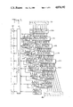
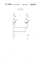
- FIG. 1 is a block diagram of a divider in accordance with one embodiment of the invention.
- FIG. 2 is a block diagram of one embodiment of each of the partial remainder determining circuits of the divider of FIG. 1;
- FIG. 3 is a circuit diagram showing a CMOS circuit which defines the basic cell shown in FIG. 2;
- FIG. 4 is a circuit diagram of an embodiment of the transfer gate shown within broken lines in FIG. 3;
- FIG. 5 is a circuit diagram of an embodiment of the initial partial remainder determining circuit of FIG. 1;
- FIG. 6 is a circuit diagram showing a CMOS circuit which defines the quotient-determining circuit shown in FIG. 1.
- a dividend within the broken-line block 20 (hereinafter referred to as "dividend 20") is input to an initial partial remainder determining circuit 100 in the form of signals respectively corresponding to values x 1 , x 2 , . . . , x n for the 1st, 2nd, . . . , n-th digits to the right of the decimal point.
- a divisor within the broken-line box 40 (hereinafter referred to as "divisor 40") is input to the initial partial remainder determining circuit 100 and to the partial remainder determining circuits 101, 102, 103, 104, 105, . . . in the form of signals representing values y 1 , y 2 , . . . , y n for the 1st, 2nd, . . . , n-th digits to the right of the decimal point.
- a quotient within broken-line block 60 (hereinafter referred to as "quotient 60") is output from an r-radix conversion circuit 10 in the form of an r-radix number consisting of the 1st integral digit z 0 and the 1st decimal digit z 1 , the second decimal digit z 2 , . . . , the n-th decimal digit z n .
- the initial partial remainder determining circuit 100 receives dividend 20, [0.x 1 x 2 . . . x n ] r , and divisor 40, [0.y 1 y 2 . . .
- Each of the partial remainder determining circuits 101, 102, 103, 104, 105 . . . receives the output of a respective partial remainder determining circuit (or the initial partial remainder determining circuit 100) which is immediately above it as viewed in FIG. 1, together with the divisor 40 and a respective control signal 251, 252, 253, 254, 255 . . . which is output from a respective quotient-determining cell 201, 202, 203, 204, 205 . . . disposed adjacent to a respective partial remainder determining circuit 101, 102, 103, 104, 105 . . . , and outputs a partial remainder or a value obtained by inverting the sign of the partial remainder, which is then input to a subsequent (i.e., lower) partial remainder determining circuit.
- Each of the quotient-determining cells 201, 202, 203, 204, 205 . . . receives at its inputs the three most significant digits of a partial remainder, or a value obtained by inverting the sign of this partial remainder, output from the partial remainder determining circuit immediately above the respective quotient-determining cell (e.g., from the (j-1)th partial remainder determining circuit), together with the value of the j-1th decimal digit of the quotient in the SD expression which has been determined in the quotient-determining cell immediately above (i.e., the (j-1)th quotient-determining cell), and outputs the value for the j-th decimal digit of the quotient, together with the respective control signal 251, 252, 253, 254, 255 . . . , which is supplied to the partial remainder determining circuit in the same stage (i.e., the j-th stage).
- the r-radix conversion circuit 10 receives at its inputs the digits of a quotient in the SD expression which have been determined in quotient-determining cells 201, 202, 203, 204, 205 . . . , respectively, and outputs a quotient 60, [z 0 .z 1 z 2 . . . z n ] r , which is an ordinary r-radix number in which each digit is non-negative.
- A.sup.(1) is determined in initial partial remainder determining circuit 100 as follows:
- the j-th decimal q j of the quotient is determined in accordance with the value of the most significant three digits [a 0 j .a 1 j a 2 j ] SD2 of the partial remainder A.sup.(j) and the j-1th decimal digit q j-1 of the quotient in the j-th cell of the quotient-determining cells 201, 202, 203, 204, 205 . . . .
- D.sup.(j) is a binary number in both cases.
- each digit is a non-negative redundant binary number.
- each of the partial remainder determining circuits 101, 102, 103, 104, 105 . . . can be implemented using an addition circuit which handles redundant binary number and a conventional binary number each digit of which is non-negative, a circuit which inverts a redundant binary number and a circuit which determines an addend.
- each of the control signals 251, 252, 253, 254, 255 . . . which are delivered to the corresponding partial remainder determining circuits is formed in accordance with the magnitude of the corresponding quotient digit q j and as to whether or not -q j and -q j-1 are different from each other in terms of sign.
- the converter 10 executes a normal subtraction (Q + -Q - ) of a non-signed binary number Q - , which is obtained by setting only the -1 digits of the quotient Q in the redundant binary expression to 1, from a non-signed binary number Q + , which is obtained by setting only the 1 digits of the quotient Q to 1, and can be implemented by ripple-carry addition circuitry or carry look ahead addition circuitry.
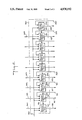
- FIG. 2 is a block diagram showing an embodiment of the partial remainder determining circuits 101, 102, 103, 104, 105 . . . of FIG. 1.
- a partial remainder determining circuit 300 is defined by an array of n+1 redundant addition cells 310, 311, 312, 313 . . . 329, 330. Assuming that partial remainder determining circuit 300 is the j-th partial remainder determining circuit in the embodiment shown in FIG. 1, inputs 340, 341, 342, 340, 341, 342, 343, . . . 359 corresponding to augends respectively represent values for digits a 1 j , a 2 j , . . .
- Control signal 390 is one of the control signals 251, 252 . . . shown in FIG. 1 and is determined in accordance with the previously determined digit q j or q j-1 of the quotient in the quotient-determining cell in the same stage (i.e., the j-th stage).
- Outputs 410, 411, 412, . . . , 430 of redundant addition cells 310, 311, 312, . . . , 330 respectively represent the values of digits a 0 j+1 , a 1 j+1 , a 2 j+1 , . . . , a n j+1 of the partial remainder.
- the carry 450 from the final digit may also be omitted.
- Redundant addition cells 310, 311, 312, 313, . . . , 329, 330 determine the 1st integral digit, the 1st decimal digit, the 2nd decimal digit, . . . , the n-th decimal digit, respectively, of the partial remainder A.sup.(j+1). Of these redundant addition cells, cells 312, 313, . . .
- 329 for the 2nd decimal digit to the (n-1)th decimal digit may be constituted by basic cells for the purpose of reducing the number of elements required, and cells 310 and 311 for the most two significant digits and cell 330 for the least significant digit (i.e., the n-th decimal digit) may be constituted by higher order cells.
- redundant addition cells 310 and 311 for the two most significant digits may be combined with the quotient-determining cell in the same stage (i.e., the j-th stage) to form a single cell, or redundant addition cell 330 for the least significant digit in the j-th stage and redundant addition cell 329 for the n-1th decimal digit in the j+1th stage may be combined together to form a single cell, for the purpose of reducing the number of elements. It is also possible to omit redundant addition cells for each 2 ⁇ (n-j+1)th decimal digit in the j-th partial remainder determining circuit for integers j in the range n/2 ⁇ j ⁇ n-1. FIG. 1 shows a first embodiment with such redundant addition cells omitted.
- One digit a i j , or q j in a redundant binary expression is expressed by two bits a i+ j a i- j , or q j+ q j- , respectively, and -1, 0 and 1 binary-coded into 11, 10 and 01, respectively.
- the magnitude and sign of the j-th decimal digit q j of the quotient can be represented by q j- and q j+ , respectively.
- the signal which indicates whether or not there is a difference in sign between the j-th decimal digit q j and (j-1)th decimal digit q j-1 of the quotient is denoted t j .
- q j- and q j+ can be determined according to the following equations, respectively: ##EQU5## where ".”, “+” and “ ⁇ ” represent logical product (AND), logical sum (OR) and exclusive logical sum (EX-OR), respectively, and ##EQU6## are operators representing logical negation a i- j +a i+ j and q j- , respectively.
- the i-th decimal digit d i j of the addend D.sup.(j), the intermediate sum S i j , and the intermediate carry C i j can be determined according to the following equations, respectively: ##EQU7##
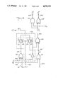
- FIG. 3 is a circuit diagram of an embodiment of a basic addition cell 312, 313, . . . 329 of FIG. 2 implemented by CMOS circuitry by virtue of the binary coding described above.
- Gates 611 and 625 are EX-OR gates.
- Gate 612 is an inverter
- gate 613 is two-input NOR gate
- gate 631 is a two-input NAND gate
- gate 632 is an EX-NOR gate.
- a p-channel transistor 621/n-channel transistor 622 pair and p-channel transistor 623/n-channel transistor 624 pair constitute transfer gates, respectively.
- a i+1+ j on input 601 and a i-1+ j on input 602 constitute in combination the 2-bit input signal 340, 341, . . . 359 to the i+1th redundant addition cell shown in FIG. 2, and logical negation y i on input 603 of the i-th decimal digit digit y i is the 1-bit input signal 361, 362 . . . 380 to that cell, as shown in FIG. 2.
- Signals q j- on input 604 and t j on input 605 constitute in combination the 2-bit control signal 390 shown in FIG. 2.
- Signal on output 614 of gate 613 corresponds to the addend d i j .
- the signals on line 615 (input of gate 611) and on line 602 (output of transistor pairs) represent data corresponding to the augend T.sup.(j) (a i+1 j ).
- Signal S i j on output 626 is a 1-bit signal which represents an intermediate sum.
- Signals C i j on output 627 of the transistor pair indicates whether there is an intermediate carry, and signal C i+1 j on inputs 628 to gates 631 and 632 indicates whether or not there is an intermediate carry from the next lower order digit.
- Signals a 1+ j+1 on output 633 of gate 631 and a 1- j+1 on output 634 of gate 632 constitute in combination 2-bit signals 410, 411, 412 . . . 430 representing the i-th decimal digit of the partial remainder.
- the added determining means for outputting the divisor y i in place of 0 in response to the 1-bit signal g j- representing the magnitude of the j-th decimal digit g j of the quotient is implemented by NOR gate 613.
- the means for inverting the sign of the augend is implemented by exclusive OR gate 611.
- the intermediate sum determining circuit is constructed of exclusive OR gate 625 and the inverter 612, and the intermediate carry determining circuit (first circuit) is construced of switch circuitry composed of the transfer gates 621 and 622, transfer gates 623 and 624, and inverter 612.
- the circuit which receives the 1-bit signal S 1 j representing the intermediate sum and the 1-bit signal C i+1 j representing the intermediate carry from the lower-order digits and which outputs the final sum 2-bit signal a i+ j+1 and a i- j-1 is constructed of the NAND gate 631 and the exclusive NOR gate 632.
- FIG. 4 shows an embodiment of the transfer gate portion 700 of the circuit shown in FIG. 3 in which portion 700 is constituted by NOR gates.
- Gates 701, 702 and 703 are 2-input NOR gates, while gates 701, 702 and 703 with inverter 612 constitute an intermediate carry determining circuit.
- composite gates may be employed to implement circuit portion 700 of FIG. 3.
- the initial partial remainder determining circuit 100 may have its individual cells simplified by always setting the intermediate carry of each digit at 0, because of ordinary redundant subtraction of binary numbers or redundant addition of non-positive redundant binary numbers.
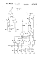
- FIG. 5 depicts an embodiment of a redundant subtraction circuit (or cell) for binary numbers (i.e., x i and y i ) which may be used in the construction of the initial partial remainder determining circuit 100.
- Signal 711 is a 1-bit signal x i representing the i-th decimal digit of the dividend
- signal 712 is a 1-bit signal y i representing the logical negation of the i-th decimal digit of the divisor
- signals 731 and 732 are 2-bit signals a i+ 1 and a i- 1 representing the i-th decimal digit of the initial partial remainder A.sup.(1).
- the redundant subtraction circuit (or cell) is constructed of 2-input NAND circuit 721 and exclusive NOR circuit 722.
- gate 811 is an inverter
- gates 813 and 823 are two-input NOR gates
- gates 814, 815 and 822 are three-input NOR gates
- gates 812 and 821 are four-input NOR gates
- gate 831 is an EX-NOR gate.
- Signal a 0+ j on input 801 and signal a 0- j on input 802 constitute in combination the 2-bit input signal 410 shown in FIG. 2; signal a 1+ j on output 803 and signal a 1- j on output 804 constitute the 2-bit input signal 411; and signal a 2+ j on input 805 and signal a 2- j on input 806 constitute the 2-bit input signal 412.
- Signal q j-1+ on output 807 corresponds to input signals 271, 272, 273 . . . , from higher-order quotient determining cells shown in FIG. 1.
- Signal q j+ on output 832 and signal q j- on output 833 constitute in combination a 2-bit signal representing the j-th decimal digit of the quotient; and signal q j- on output 833 and signal t j on output 834 constitute the 2-bit signal for controlling the redundant addition cells 310, 311, 312, . . . 350 in the j-th stage.
- Quotient determining means may comprise inverter 811 and NOR gates 813, 814, 822 and 815 in FIG. 6, and sign inversion means may comprise NOR gate 823 and EX-NOR gate 831 in FIG. 6.
- the 1-bit signal t j of the 2-bit control signal 390 is provided by inverter 811 and NOR gates 812, 813, 814 and 821.
- the 1-bit signal q j- 833 representing the magnitude of the quotient is used as it is for the remaining 1-bit control signal.
- CMOS circuit Although in the above-described embodiment of a CMOS circuit, the same sign is assigned to the partial remainder a i j and the quotient q j in the binary coding, these values may be binary-coded so as to have different signs. Although addition of a redundant binary number and an ordinary binary number alone has been described above, a similar embodiment can be formed with respect to subtraction.
- the number of transistors is 32, and the number of gates on the critical path is 3.
- the number of transistors is 50, and the number of gates on the critical path is 2.
- a divider can be realized by combinational CMOS circuitry having an array structure formed from regularly arranged basic cells and quotient determining cells.
- Each basic cell involves a delay in arithmetic operations required per digit of a quotient equivalent to 5 gates and includes about 30 transistors, and each quotient determining cell includes about 50 transistors.
- the divider according to the present invention has a reduced number of transistors which is substantially half of that in the conventional shift, subtract restore, divide units using prior art ripple-carry addition units, and the computing time (the number of transfer gates) is reduced to about 1/12 and about 1/24 of those of the prior art in the case of division operations with 32 bits and 64 bits, respectively. Further, the number of transistors required in the divider according to the present invention is substantially half of that of the conventional shift, subtract, restore divide units using prior art redundant binary addition and subtraction units.
- the present invention is effective in reducing the number of circuit elements required to form a divider, enabling a divider to be realized compactly on an LSI chip and increasing operational speed.
- addition and subtraction in an arithmetic operation such as division or multiplication can be implemented by combinational circuitry using either a redundant addition circuit employing, for example, numbers in the signed digit (SD) expression in which each digit is allowed to have a negative value, or a redundant subtraction circuit, and it is possible to minimize carry or borrow propagation in addition or subtraction to one digit at most, thus providing the following advantages:
- SD signed digit
- the arithmetic processor can readily and economically be realized compactly on an LSI chip.
Landscapes
- Physics & Mathematics (AREA)
- General Physics & Mathematics (AREA)
- Engineering & Computer Science (AREA)
- Computational Mathematics (AREA)
- Mathematical Analysis (AREA)
- Mathematical Optimization (AREA)
- Pure & Applied Mathematics (AREA)
- Theoretical Computer Science (AREA)
- Computing Systems (AREA)
- General Engineering & Computer Science (AREA)
- Complex Calculations (AREA)
Abstract
Description
{-1, 0, 1}; {-2, -1, 0, 1, 2}; {-N, . . . , -1, 0, 1, . . . , N},
R.sup.(j+1) =r×R.sup.(j) -q.sub.j ×D,
X=[x.sub.0.x.sub.1 . . . x.sub.n ].sub.SD2,
R.sup.(j+1) =P.sup.(j) (P.sup.(j) (r×R.sup.(j))+D.sup.(j)).
A.sup.(j+1) =T.sup.(j) (2×A.sup.(j))+D.sup.(j).
T.sup.(j) (X)=p.sup.(j) (P.sup.(j-1) (X)).
              TABLE 1
______________________________________
           Augend (Redundant Binary)
           -1       0       1
______________________________________
Addend     0     -1         0     -1
(Binary)   1     0          -1    0
______________________________________
              TABLE 2
______________________________________
           Augend (Redundant Binary)
           -1       0       1
______________________________________
Addend     0     0          0     1
(Binary)   1     0          1     1
______________________________________
K.(B.C+B.C)+K.(B.C+B.C),
K+(B.C+B.C).
A.sup.(1) =[0.x.sub.1 x.sub.2 . . . x.sub.n ].sub.SD2 +[0.y.sub.1 y.sub.2 . . . y.sub.n ].sub.SD2.
A.sup.(j+1) =T.sup.(j) (2×A.sup.(j))+D.sup.(j)
T.sup.(j) (2×A.sup.(j))=[a.sub.0.sup.j a.sub.1.sup.j.a.sub.2.sup.j . . . a.sub.n.sup.j 0].sub.SD2 ;
T.sup.(j) (2×A.sup.(j))=[b.sub.0.sup.j b.sub.1.sup.j.b.sub.2.sup.j . . . b.sub.n.sup.j 0].sub.SD2 ;
D.sup.(j) =[0.y.sub.1 y.sub.2 . . . y.sub.n ].sub.SD2 ;
D.sup.(j) =[0.00 . . . 0].sub.SD2.
t.sub.j =a.sub.0+.sup.j.(a.sub.0-.sup.j +a.sub.1+.sup.j).(a.sub.0-.sup.j +a.sub.1-.sup.j +a.sub.2+.sup.j).(a.sub.0-.sup.j +a.sub.1-.sup.j +a.sub.2-.sup.j +q.sub.j-1+).
Claims (23)
Applications Claiming Priority (4)
| Application Number | Priority Date | Filing Date | Title |
|---|---|---|---|
| JP61-164091 | 1986-07-11 | ||
| JP61164090A JPH0614317B2 (en) | 1986-07-11 | 1986-07-11 | Processor |
| JP61-164090 | 1986-07-11 | ||
| JP61164091A JPH0614318B2 (en) | 1986-07-11 | 1986-07-11 | Processor |
Related Parent Applications (2)
| Application Number | Title | Priority Date | Filing Date |
|---|---|---|---|
| US07/066,817 Continuation-In-Part US4873660A (en) | 1986-06-27 | 1987-06-25 | Arithmetic processor using redundant signed digit arithmetic |
| US07/074,892 Continuation-In-Part US4866655A (en) | 1986-07-18 | 1987-07-17 | Arithmetic processor and divider using redundant signed digit |
Related Child Applications (7)
| Application Number | Title | Priority Date | Filing Date |
|---|---|---|---|
| US07/066,817 Continuation-In-Part US4873660A (en) | 1986-06-27 | 1987-06-25 | Arithmetic processor using redundant signed digit arithmetic |
| US07/074,892 Continuation-In-Part US4866655A (en) | 1986-07-18 | 1987-07-17 | Arithmetic processor and divider using redundant signed digit |
| US07/086,967 Continuation-In-Part US4866657A (en) | 1986-07-18 | 1987-08-18 | Adder circuitry utilizing redundant signed digit operands |
| US07/136,365 Continuation-In-Part US4935892A (en) | 1986-12-24 | 1987-12-22 | Divider and arithmetic processing units using signed digit operands |
| US19931888A Continuation-In-Part | 1987-05-27 | 1988-05-26 | |
| US03/239,243 Continuation-In-Part US5031136A (en) | 1986-06-27 | 1990-05-07 | Signed-digit arithmetic processing units with binary operands |
| US07/599,275 Continuation-In-Part US5153847A (en) | 1986-06-27 | 1990-10-16 | Arithmetic processor using signed digit representation of internal operands |
Publications (1)
| Publication Number | Publication Date |
|---|---|
| US4878192A true US4878192A (en) | 1989-10-31 |
Family
ID=26489318
Family Applications (1)
| Application Number | Title | Priority Date | Filing Date |
|---|---|---|---|
| US07/070,565 Expired - Lifetime US4878192A (en) | 1986-07-11 | 1987-07-07 | Arithmetic processor and divider using redundant signed digit arithmetic |
Country Status (1)
| Country | Link |
|---|---|
| US (1) | US4878192A (en) |
Cited By (16)
| Publication number | Priority date | Publication date | Assignee | Title |
|---|---|---|---|---|
| US4985861A (en) * | 1988-01-29 | 1991-01-15 | Nec Corporation | High speed digital signal processor for signed digit numbers |
| US5031136A (en) * | 1986-06-27 | 1991-07-09 | Matsushita Electric Industrial Co., Ltd. | Signed-digit arithmetic processing units with binary operands |
| US5097434A (en) * | 1990-10-03 | 1992-03-17 | The Ohio State University Research Foundation | Hybrid signed-digit/logarithmic number system processor |
| US5282156A (en) * | 1991-01-31 | 1994-01-25 | Matsushita Electric Industrial Co., Ltd. | Leading one anticipator and floating point addition/subtraction apparatus employing same |
| US5323347A (en) * | 1991-02-19 | 1994-06-21 | Mitsubishi Denki Kabushiki Kaisha | Semiconductor memory device storing two types of binary number data and method of operating the same |
| US5365471A (en) * | 1991-08-08 | 1994-11-15 | Mitsubishi Denki Kabushiki Kaisha | Divider for performing signed division using a redundant signed digit |
| US5416733A (en) * | 1994-01-26 | 1995-05-16 | United Microelectronics Corp. | Apparatus for finding quotient in a digital system |
| US5488315A (en) * | 1995-01-05 | 1996-01-30 | Texas Instruments Incorporated | Adder-based base cell for field programmable gate arrays |
| US5847983A (en) * | 1995-08-24 | 1998-12-08 | Matsushita Electric Industrial Co., Ltd. | Full subtracter |
| US20010056454A1 (en) * | 1999-12-23 | 2001-12-27 | Bharat Bhushan | Method and apparatus for performing subtraction in redundant form arithmetic |
| US20020147755A1 (en) * | 1999-12-23 | 2002-10-10 | Bharat Bhushan | Method and apparatus for a fast comparison in redundant form arithmetic |
| US6763368B2 (en) | 1999-12-23 | 2004-07-13 | Intel Corporation | Method and apparatus for performing single-cycle addition or subtraction and comparison in redundant form arithmetic |
| US6813628B2 (en) | 1999-12-23 | 2004-11-02 | Intel Corporation | Method and apparatus for performing equality comparison in redundant form arithmetic |
| US6848043B1 (en) | 2000-04-27 | 2005-01-25 | Intel Corporation | Optimal redundant arithmetic for microprocessors design |
| US20070088774A1 (en) * | 2003-04-17 | 2007-04-19 | Zhizhong Li | Computer technical solution of mixed q-nary and carry line digital engineering method |
| US20080201394A1 (en) * | 2004-11-08 | 2008-08-21 | Zhizhong Li | Computer Technical Solution Of The Digital Engineering Method Of Hybrid Numeral Carry System And Carry Line |
-
1987
- 1987-07-07 US US07/070,565 patent/US4878192A/en not_active Expired - Lifetime
Non-Patent Citations (30)
| Title |
|---|
| A Class of Binary Divisions Yielding Minimally Represented Quotients, Metze, IRE Transactions of Electronic Computers, pp. 761 764, 12/62. * |
| A Class of Binary Divisions Yielding Minimally Represented Quotients, Metze, IRE Transactions of Electronic Computers, pp. 761-764, 12/62. |
| A New Class of Digital Division Methods, James Robertson, IRE Transactions on Electronic Computers, pp. 218 222, 9/58. * |
| A New Class of Digital Division Methods, James Robertson, IRE Transactions on Electronic Computers, pp. 218-222, 9/58. |
| A VLSI Oriented High Speed Divider Using Redundant Binary Representation, Takagi et al., IECE Japan, vol. 167.D, 4, pp. 450 457, 4/84. * |
| A VLSI Oriented High Speed Multiplier Using Redundant Binary Adder Tree, Takagi et al., IECE Japan, vol. J66.d, pp. 683 690, 6/84. * |
| A VLSI-Oriented High-Speed Divider Using Redundant Binary Representation, Takagi et al., IECE Japan, vol. 167.D, #4, pp. 450-457, 4/84. |
| A VLSI-Oriented High-Speed Multiplier Using Redundant Binary Adder Tree, Takagi et al., IECE Japan, vol. J66.d, pp. 683-690, 6/84. |
| Atkins, "Design of the Arithmetic Units of ILLIAC III: Use of Redundancy & Higher Radix Methods", IEEE Trans. on Computers, vol. C-19, No. 8, Aug. 1977, pp. 720-733. |
| Atkins, Design of the Arithmetic Units of ILLIAC III: Use of Redundancy & Higher Radix Methods , IEEE Trans. on Computers, vol. C 19, No. 8, Aug. 1977, pp. 720 733. * |
| Avizienis, "Binary-Compatible Signed-Digit Arithmetic", Proceedings-Fall Joint Computer Conference, 1964, pp. 663-672. |
| Avizienis, Binary Compatible Signed Digit Arithmetic , Proceedings Fall Joint Computer Conference, 1964, pp. 663 672. * |
| Concise Papers, Lyon, IEEE Transactions on Communications, pp. 418 425, 4/76. * |
| Concise Papers, Lyon, IEEE Transactions on Communications, pp. 418-425, 4/76. |
| Design of High Speed MOS Multiplier and Divider Using Redundant Binary Representation, Kuninobu et al., Proceedings 8th Symposium on Computer Arithmetic, pp. 80 86, 5/87. * |
| Design of High Speed MOS Multiplier and Divider Using Redundant Binary Representation, Kuninobu et al., Proceedings 8th Symposium on Computer Arithmetic, pp. 80-86, 5/87. |
| Design of the Arithmetic Units of ILLIAC III, Redundancy & Higher Radix Methods, Atkins, IEEE Transacts. on Computers, vol. C 19, pp. 720 732, 8/70. * |
| Design of the Arithmetic Units of ILLIAC III, Redundancy & Higher Radix Methods, Atkins, IEEE Transacts. on Computers, vol. C-19, pp. 720-732, 8/70. |
| High Speed Multiplier Using A Redundant Binary Adder Tree, Harata et al., IEEE International Conference on Computer Design, pp. 165 170, 1984. * |
| High Speed Multiplier Using A Redundant Binary Adder Tree, Harata et al., IEEE International Conference on Computer Design, pp. 165-170, 1984. |
| High Speed VLSI Multiplication Algorithm with a Redundant Binary Addition Tree, Takagi et al., IEEE Transactions on Computers, vol. C 34, No. 9, pp. 1789 1795, 9/85. * |
| High Speed VLSI Multiplication Algorithm with a Redundant Binary Addition Tree, Takagi et al., IEEE Transactions on Computers, vol. C-34, No. 9, pp. 1789-1795, 9/85. |
| Multiple OPerand Addition and Multiplication, Shanker Singh et al., IEEE Transactions on Computers, vol. C 22, No. 2, pp. 113 120, 2/73. * |
| Multiple OPerand Addition and Multiplication, Shanker Singh et al., IEEE Transactions on Computers, vol. C-22, No. 2, pp. 113-120, 2/73. |
| Real Time Processing Gains Ground with Fast Digital Multiplier, Waser et al., Electronics, pp. 93 99, 9/77. * |
| Real-Time Processing Gains Ground with Fast Digital Multiplier, Waser et al., Electronics, pp. 93-99, 9/77. |
| Signed Digit Number Representations for Fast Parallel Arithmetic, Avizienis, IRE Transactions on Electronic Computers, pp. 389 400, 9/61. * |
| Signed-Digit Number Representations for Fast Parallel Arithmetic, Avizienis, IRE Transactions on Electronic Computers, pp. 389-400, 9/61. |
| Tung, "Division Algorithm for Signed-Digit Arithmetic", IEEE Trans. on Computers, Sep. 1968, pp. 887-889. |
| Tung, Division Algorithm for Signed Digit Arithmetic , IEEE Trans. on Computers, Sep. 1968, pp. 887 889. * |
Cited By (21)
| Publication number | Priority date | Publication date | Assignee | Title |
|---|---|---|---|---|
| US5031136A (en) * | 1986-06-27 | 1991-07-09 | Matsushita Electric Industrial Co., Ltd. | Signed-digit arithmetic processing units with binary operands |
| US4985861A (en) * | 1988-01-29 | 1991-01-15 | Nec Corporation | High speed digital signal processor for signed digit numbers |
| US5097434A (en) * | 1990-10-03 | 1992-03-17 | The Ohio State University Research Foundation | Hybrid signed-digit/logarithmic number system processor |
| US5282156A (en) * | 1991-01-31 | 1994-01-25 | Matsushita Electric Industrial Co., Ltd. | Leading one anticipator and floating point addition/subtraction apparatus employing same |
| US5323347A (en) * | 1991-02-19 | 1994-06-21 | Mitsubishi Denki Kabushiki Kaisha | Semiconductor memory device storing two types of binary number data and method of operating the same |
| US5365471A (en) * | 1991-08-08 | 1994-11-15 | Mitsubishi Denki Kabushiki Kaisha | Divider for performing signed division using a redundant signed digit |
| US5416733A (en) * | 1994-01-26 | 1995-05-16 | United Microelectronics Corp. | Apparatus for finding quotient in a digital system |
| US5488315A (en) * | 1995-01-05 | 1996-01-30 | Texas Instruments Incorporated | Adder-based base cell for field programmable gate arrays |
| US5847983A (en) * | 1995-08-24 | 1998-12-08 | Matsushita Electric Industrial Co., Ltd. | Full subtracter |
| US20020147755A1 (en) * | 1999-12-23 | 2002-10-10 | Bharat Bhushan | Method and apparatus for a fast comparison in redundant form arithmetic |
| US20010056454A1 (en) * | 1999-12-23 | 2001-12-27 | Bharat Bhushan | Method and apparatus for performing subtraction in redundant form arithmetic |
| US6754689B2 (en) * | 1999-12-23 | 2004-06-22 | Intel Corporation | Method and apparatus for performing subtraction in redundant form arithmetic |
| US6763368B2 (en) | 1999-12-23 | 2004-07-13 | Intel Corporation | Method and apparatus for performing single-cycle addition or subtraction and comparison in redundant form arithmetic |
| US6813628B2 (en) | 1999-12-23 | 2004-11-02 | Intel Corporation | Method and apparatus for performing equality comparison in redundant form arithmetic |
| US6826588B2 (en) * | 1999-12-23 | 2004-11-30 | Intel Corporation | Method and apparatus for a fast comparison in redundant form arithmetic |
| US20040267863A1 (en) * | 1999-12-23 | 2004-12-30 | Bharat Bhushan | Method and apparatus for performing single-cycle addition or subtraction and comparison in redundant form arithmetic |
| US7395304B2 (en) | 1999-12-23 | 2008-07-01 | Intel Corporation | Method and apparatus for performing single-cycle addition or subtraction and comparison in redundant form arithmetic |
| US6848043B1 (en) | 2000-04-27 | 2005-01-25 | Intel Corporation | Optimal redundant arithmetic for microprocessors design |
| US20070088774A1 (en) * | 2003-04-17 | 2007-04-19 | Zhizhong Li | Computer technical solution of mixed q-nary and carry line digital engineering method |
| US20080201394A1 (en) * | 2004-11-08 | 2008-08-21 | Zhizhong Li | Computer Technical Solution Of The Digital Engineering Method Of Hybrid Numeral Carry System And Carry Line |
| US8341203B2 (en) | 2004-11-08 | 2012-12-25 | Zhizhong Li | Computer technical solution of the digital engineering method of hybrid numeral carry system and carry line |
Similar Documents
| Publication | Publication Date | Title |
|---|---|---|
| US4878192A (en) | Arithmetic processor and divider using redundant signed digit arithmetic | |
| US3610906A (en) | Binary multiplication utilizing squaring techniques | |
| US4363107A (en) | Binary multiplication cell circuit | |
| JP3436994B2 (en) | Shift device | |
| US4873660A (en) | Arithmetic processor using redundant signed digit arithmetic | |
| US4866655A (en) | Arithmetic processor and divider using redundant signed digit | |
| JPH08161152A (en) | Floating point arithmetic unit | |
| Ganguly et al. | A unified flagged prefix constant addition-subtraction scheme for design of area and power efficient binary floating-point and constant integer arithmetic circuits | |
| US4866657A (en) | Adder circuitry utilizing redundant signed digit operands | |
| US4935892A (en) | Divider and arithmetic processing units using signed digit operands | |
| US4890127A (en) | Signed digit adder circuit | |
| US5206825A (en) | Arithmetic processor using signed-digit representation of external operands | |
| US5153847A (en) | Arithmetic processor using signed digit representation of internal operands | |
| US5031136A (en) | Signed-digit arithmetic processing units with binary operands | |
| US3462589A (en) | Parallel digital arithmetic unit utilizing a signed-digit format | |
| US4979140A (en) | Signed digit adder circuit | |
| JPH0528407B2 (en) | ||
| JPH0582609B2 (en) | ||
| JPH06230933A (en) | Processor | |
| JPH061437B2 (en) | Processor | |
| JPH061435B2 (en) | Processor | |
| JPH0614318B2 (en) | Processor | |
| JPH061433B2 (en) | Processor | |
| JP2681968B2 (en) | Arithmetic processing unit | |
| Bindal | Review of Combinational Logic Circuits |
Legal Events
| Date | Code | Title | Description |
|---|---|---|---|
| AS | Assignment |
Owner name: MATSUSHITA ELECTRIC INDUSTRIAL CO., LTD., 1006 OAZ Free format text: ASSIGNMENT OF ASSIGNORS INTEREST.;ASSIGNORS:NISHIYAMA, TAMOTSU;KUNINOBU, SHIGEO;REEL/FRAME:004759/0517 Effective date: 19870701 Owner name: MATSUSHITA ELECTRIC INDUSTRIAL CO.,JAPAN Free format text: ASSIGNMENT OF ASSIGNORS INTEREST;ASSIGNORS:NISHIYAMA, TAMOTSU;KUNINOBU, SHIGEO;REEL/FRAME:004759/0517 Effective date: 19870701 |
|
| STCF | Information on status: patent grant |
Free format text: PATENTED CASE |
|
| FEPP | Fee payment procedure |
Free format text: PAYOR NUMBER ASSIGNED (ORIGINAL EVENT CODE: ASPN); ENTITY STATUS OF PATENT OWNER: LARGE ENTITY |
|
| FEPP | Fee payment procedure |
Free format text: PAYER NUMBER DE-ASSIGNED (ORIGINAL EVENT CODE: RMPN); ENTITY STATUS OF PATENT OWNER: LARGE ENTITY Free format text: PAYOR NUMBER ASSIGNED (ORIGINAL EVENT CODE: ASPN); ENTITY STATUS OF PATENT OWNER: LARGE ENTITY |
|
| FPAY | Fee payment |
Year of fee payment: 4 |
|
| CC | Certificate of correction | ||
| FPAY | Fee payment |
Year of fee payment: 8 |
|
| FPAY | Fee payment |
Year of fee payment: 12 |