US4835112A - CMOS salicide process using germanium implantation - Google Patents
CMOS salicide process using germanium implantation Download PDFInfo
- Publication number
- US4835112A US4835112A US07/165,678 US16567888A US4835112A US 4835112 A US4835112 A US 4835112A US 16567888 A US16567888 A US 16567888A US 4835112 A US4835112 A US 4835112A
- Authority
- US
- United States
- Prior art keywords
- drain regions
- semiconductor substrate
- source
- dopant
- dielectric layer
- Prior art date
- Legal status (The legal status is an assumption and is not a legal conclusion. Google has not performed a legal analysis and makes no representation as to the accuracy of the status listed.)
- Expired - Lifetime
Links
Images


Classifications
-
- H10P30/204—
-
- H—ELECTRICITY
- H10—SEMICONDUCTOR DEVICES; ELECTRIC SOLID-STATE DEVICES NOT OTHERWISE PROVIDED FOR
- H10D—INORGANIC ELECTRIC SEMICONDUCTOR DEVICES
- H10D30/00—Field-effect transistors [FET]
- H10D30/01—Manufacture or treatment
- H10D30/021—Manufacture or treatment of FETs having insulated gates [IGFET]
- H10D30/0223—Manufacture or treatment of FETs having insulated gates [IGFET] having source and drain regions or source and drain extensions self-aligned to sides of the gate
- H10D30/0227—Manufacture or treatment of FETs having insulated gates [IGFET] having source and drain regions or source and drain extensions self-aligned to sides of the gate having both lightly-doped source and drain extensions and source and drain regions self-aligned to the sides of the gate, e.g. lightly-doped drain [LDD] MOSFET or double-diffused drain [DDD] MOSFET
-
- H—ELECTRICITY
- H10—SEMICONDUCTOR DEVICES; ELECTRIC SOLID-STATE DEVICES NOT OTHERWISE PROVIDED FOR
- H10D—INORGANIC ELECTRIC SEMICONDUCTOR DEVICES
- H10D30/00—Field-effect transistors [FET]
- H10D30/60—Insulated-gate field-effect transistors [IGFET]
-
- H—ELECTRICITY
- H10—SEMICONDUCTOR DEVICES; ELECTRIC SOLID-STATE DEVICES NOT OTHERWISE PROVIDED FOR
- H10D—INORGANIC ELECTRIC SEMICONDUCTOR DEVICES
- H10D62/00—Semiconductor bodies, or regions thereof, of devices having potential barriers
- H10D62/10—Shapes, relative sizes or dispositions of the regions of the semiconductor bodies; Shapes of the semiconductor bodies
- H10D62/13—Semiconductor regions connected to electrodes carrying current to be rectified, amplified or switched, e.g. source or drain regions
- H10D62/149—Source or drain regions of field-effect devices
- H10D62/151—Source or drain regions of field-effect devices of IGFETs
-
- H—ELECTRICITY
- H10—SEMICONDUCTOR DEVICES; ELECTRIC SOLID-STATE DEVICES NOT OTHERWISE PROVIDED FOR
- H10D—INORGANIC ELECTRIC SEMICONDUCTOR DEVICES
- H10D84/00—Integrated devices formed in or on semiconductor substrates that comprise only semiconducting layers, e.g. on Si wafers or on GaAs-on-Si wafers
- H10D84/01—Manufacture or treatment
- H10D84/0123—Integrating together multiple components covered by H10D12/00 or H10D30/00, e.g. integrating multiple IGBTs
- H10D84/0126—Integrating together multiple components covered by H10D12/00 or H10D30/00, e.g. integrating multiple IGBTs the components including insulated gates, e.g. IGFETs
- H10D84/0165—Integrating together multiple components covered by H10D12/00 or H10D30/00, e.g. integrating multiple IGBTs the components including insulated gates, e.g. IGFETs the components including complementary IGFETs, e.g. CMOS devices
- H10D84/0172—Manufacturing their gate conductors
- H10D84/0174—Manufacturing their gate conductors the gate conductors being silicided
-
- H—ELECTRICITY
- H10—SEMICONDUCTOR DEVICES; ELECTRIC SOLID-STATE DEVICES NOT OTHERWISE PROVIDED FOR
- H10D—INORGANIC ELECTRIC SEMICONDUCTOR DEVICES
- H10D84/00—Integrated devices formed in or on semiconductor substrates that comprise only semiconducting layers, e.g. on Si wafers or on GaAs-on-Si wafers
- H10D84/01—Manufacture or treatment
- H10D84/02—Manufacture or treatment characterised by using material-based technologies
- H10D84/03—Manufacture or treatment characterised by using material-based technologies using Group IV technology, e.g. silicon technology or silicon-carbide [SiC] technology
- H10D84/038—Manufacture or treatment characterised by using material-based technologies using Group IV technology, e.g. silicon technology or silicon-carbide [SiC] technology using silicon technology, e.g. SiGe
-
- H10P30/208—
-
- H10P30/212—
-
- H10P32/00—
-
- Y—GENERAL TAGGING OF NEW TECHNOLOGICAL DEVELOPMENTS; GENERAL TAGGING OF CROSS-SECTIONAL TECHNOLOGIES SPANNING OVER SEVERAL SECTIONS OF THE IPC; TECHNICAL SUBJECTS COVERED BY FORMER USPC CROSS-REFERENCE ART COLLECTIONS [XRACs] AND DIGESTS
- Y10—TECHNICAL SUBJECTS COVERED BY FORMER USPC
- Y10S—TECHNICAL SUBJECTS COVERED BY FORMER USPC CROSS-REFERENCE ART COLLECTIONS [XRACs] AND DIGESTS
- Y10S257/00—Active solid-state devices, e.g. transistors, solid-state diodes
- Y10S257/90—MOSFET type gate sidewall insulating spacer
Definitions
- the invention relates to the fabrication of metal-oxide-semiconductor (MOS) transistors, and more particularly relates, in one aspect, to the fabrication of MOS transistors having source/drain regions with shallow junction depths and a refractory metal silicide contact to the source/drain regions.
- MOS metal-oxide-semiconductor
- HCI hot carrier instability
- HCI into gate insulators is a universal problem for small geometry FETs (channel lengths less than or equal to 1 ⁇ m), since most hot carriers are trapped within approximately 100 ⁇ of the semiconductor surface.
- GSD graded drain structure
- a heavily doped drain of phosphorous or arsenic surrounded by a lighter doping of phosphorus is used to gradually extend the drain region into the channel region to reduce the electric field strength right at the drain.
- this approach can be undesirable in that it causes larger overlap capacitance with the gate, larger lateral diffusion and channel shortening.
- merely the deeper junction of the drain produces more disadvantageous short channel effects, such as an abrupt drop off of threshold voltage with the effective channel length (L eff ).
- the drain is preferred to be shallow and laterally graded as to profile as well as concentration. That is, it is desired for the drain profile to have a gradual decrease in surface concentration from the n + regions to the channel region. Less desirable is the profile shape where the source/drain regions exhibit similar lateral grading but with deeper vertical junctions. With deeper junctions, there is a wider subsurface depletion effect and it is easier for the field lines to go from the drain to the source, which causes "punchthrough current" problems and shorts out the device.
- LDDs lightly doped drains
- LDDs consist of a lightly doped source/drain region that is driven just under the gate region, while the heavily doped drain region is laterally displaced away from the gate by used of a sidewall spacer on the gate.
- LDDs are advantageous because they do not have problems with excess lateral or vertical impurity diffusion.
- the process for making LDDs can be complex, and typically requires the formation of a sidewall spacer on the gate to provide the exact horizontal and/or lateral displacement of the lightly and heavily doped drain sections. That is, in LDDs, the n - portion of the source/drain region is aligned to the polysilicon gate edge, and the n + portion of the source/drain region is aligned to a spacer edge.
- DDD double diffused drain
- arsenic and phosphorus are implanted together, or are introduced into the same area, and are diffused together to form the source/drain structure. That is, both the n - and n + portions of the source/drain regions are aligned to the polysilicon gate edge.
- the process for making DDDs is very simple compared to that for making graded source/drains or LDDs in that the impurity introduction is performed essentially all at one time, and the anneal for both phosphorus and arsenic is performed together.
- the disadvantage with the DDD structure is that due to cooperative diffusion effects, phosphorus tends to diffuse faster in the presence of high arsenic doping, even faster than phosphorus diffuses alone. This undesirable effect that enhances the phosphorus diffusion discourages the use of arsenic and phosphorus together in a DDD, and phosphorus alone or GSDs and LDDs are used instead.
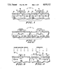
- FIG. 2 Shown in FIG. 2 is a pair of prior art MOSFETs 10 on a semiconductor substrate 12, such as silicon, covered by a thin gate dielectric material 14.
- the substrate 12 may be a well within a wafer or expitaxial layer, or an epitaxial layer itself, and that for PMOS devices the substrate 12 is n-type as shown in the right side of FIG. 1 and for NMOS devices, the substrate 12 is p-type as shown on the left.
- Upon the thin gate dielectric material 14 is a patterned gate material 15 having opposing sides adjacent which are source/drain regions 16 through 19.
- the source/drain regions 16, and especially n - and p - source/drain regions 17 are deeper than desired due to the accelerated phosphorus diffusion of heavily doped phosphorus, and thus these LDDs suffer from the same disadvantages as the graded source/drains with deep junctions discussed above.
- the same accelerated diffusion phenomenon is observed for boron in the source/drain regions 18 and 19 of the PMOS devices, but to a lesser degree.
- a particular need is to provide a workable salicided twin-tub CMOS process.
- salicide and “silicidation” as used herein refer to the formation of a self-aligned refractory metal silicide on a silicon surface through the reaction of a refractory metal with the silicon surface.
- the surface may be amorphous, polycrystalline or monocrystalline silicon.
- Salicidation of shallow junctions has been shown to result in increased leakage current with can be aggravated by the isolation edge pull back for a LOCOS (local oxidation of silicon) based isolation. Additional source/drain implantation after titanium deposition either before or after silicidation have been proposed to minimize these problems.
- LOCOS local oxidation of silicon
- the high dose phosphorus and boron implants which are performed through the silicide layer to form the n + and p + regions result in an enhanced diffusivity in the n - and p - regions causing anomalously deep source/drain junctions with degraded device punchthrough leakage.
- This is confirmed by electrical measurements in which an increase in the electrical channel length by 0.15 ⁇ m and a corresponding decrease in punchthrough leakage are observed when arsenic is used instead of phosphorus for the n + source/drain implant.
- high implant energies such as 190 keV are required to see improvements in short-channel effects while maintaining low diode leakage and contact resistance.
- arsenic may be employed in a salicided CMOS process by implantation through the silicided layers after the phosphorus has been placed if a thin enough silicide is used.
- such thin silicide layers have the disadvantage of high sheet resistance which is not desired for the circuit speed.
- CMOS FETs with low junction leakage and good short-channel effects.
- the MOSFET 10 would have source/drain regions with a profile more like the shallow profiles shown by n + source/drain regions 44 and n - source/drain regions 42 in the improved MOSFET 20 of the invention illustrated in FIG. 1.
- the source/drain regions 42 and 44 have the desired profile, satisfactory lateral grading with shallow vertical junction depths.
- the presence of germanium in regions 42 and 44 helps retard the phosphorus diffusions.
- Corresponding regions 46 and 48 for the PMOS devices are also shallower, although as noted earlier the compensating effect of the germanium is not as great for boron.
- the edges of the source/drain regions also have sufficient concentration just beneath the gate. In the LDD structures of FIG.
- the n-type and p-type impurity regions 17 and 19, respectively, are deeper into the substrate 12 region. It will be appreciated that in the structure of FIG. 1, the primary impurity concentration remains at the surface of the semiconductor substrate, rather than undesirably deeper as in prior structures. It would thus be advantageous if a process could be devised with would produce source/drain regions that would help solve HCI effects, but also be less susceptible to unwanted diffusion, as well as be easy to manufacture.
- a process for fabricating a FET on a semiconductor substrate involving first providing a semiconductor substrate having a surface and then providing a dielectric layer over the surface of the semiconductor substrate. Next, a conductive gate is provided on the dielectric layer. Then, germanium is introduced into selected regions of the semiconductor substrate on either side of the conductive gate in future source/drain regions. At least a portion of the dielectric layer is removed over the future source/drain regions to form openings. Refractory metal silicide layers are next formed in the openings in the dielectric layer over the future source/drain regions. A conductivity altering dopant is then introduced into the future source/drain regions in the substrate. Finally, the substrate is annealed to drive-in the conductivity altering dopant to form source/drain regions, whereby the diffusion of the dopant is retarded by the presence of the germanium.
- FIG. 1 is a cross sectional illustration of the CMOS FET structure of the present invention in its finished state
- FIG. 2 is a cross sectional illustration of a prior art CMOS FET structure
- FIG. 3 is a cross sectional illustration of one half of CMOS FET structure of the invention being fabricated at early stage;
- FIG. 4 is a cross sectional illustration of the CMOS FET under construction from FIG. 3 during the germanium introduction in one of the process aspects;
- FIG. 5 is a cross sectional illustration of the CMOS FET of FIG. 4 after a refractory metal has been provided thereon;
- FIG. 6 is a cross sectional illustration of the CMOS FET of FIG. 5 during introduction of the high impurity level source/drain regions;
- FIG. 7 is a cross sectional illustration of an alternate process embodiment where the germanium is introduced early in the fabrication process
- FIG. 8 is a cross sectional illustration of another alternate process aspect of the invention where the germanium is co-introduced into the substrate through the refractory metal silicide along with the dopant for the relatively heavily doped source/drain regions;
- FIG. 9 is a plot of dopant concentration with junction depth for simulated and experimental cases of phosphorus only, and phosphorus plus germanium for an n + source/drain profile
- FIG. 10 is histogram plot of the number of die with a particular L eff for NMOS devices with phosphorus only source/drains as compared with NMOS devices with both germanium and phosphorus in the source/drains;
- FIG. 11 is histogram plot of the number of die with a particular off current (I off ) as a function of leakage capacitance for NMOS devices with phosphorus only source/drains as compared with NMOS devices with both germanium and phosphorus in the source/drains.
- n + and p + dopants after titanium salicidation are employed to fabricate devices with low junction leakage and good short-channel effects.
- the diffusion for the n + junction depths can be limited even if phosphorus is the only dopant used.
- LTO low temperature oxide
- a germanium implant with doses ranging from 1E15 to 5E15 cm -2 is performed prior to the refractory metal deposition, which may be titanium, for example, and salicidation. Phosphorus and boron are then selectively implanted through the titanium silicide layer to form the n + and p + source/drain regions, respectively.
- Split wafer lots on the n + and p + implant energy were fabricated to examine trade-offs between junction quality and short-channel device behavior. As the implant energy increased, junction leakage and contact resistance are reduced at the expense of degraded short-channel effects due to the deeper junctions caused by additional dopant which is implanted through the silicide layer into the silicon substrate.
- FIG. 3 The starting point of one embodiment of the process for fabricating the CMOS FETs 20 of the present invention is shown in FIG. 3. Fabrication of only one of the device types will be described, since the processing steps for the devices of the other type is essentially identical except for the dopants used.
- FIGS. indicate in parentheses that the impurity of the other conductivity type will form the devices of the other type.
- a semiconductor substrate 22 is provided over which a dielectric layer 24 is formed.
- Semiconductor substrate has two lightly doped portions or wells 22A and 22B, which are p-wells and n-wells, respectively, for NMOS and PMOS devices, respectively.
- Conductive gates 26 are then provided on the dielectric layer 24 by forming a uniform layer and then patterning with conventional photolithographic techniques.
- the substrate 22 may be monocrystalline silicon
- the dielectric layer 24 may be silicon dioxide or silicon nitride or a combination of the two
- the conductive gates may be doped polycrystalline silicon, although it will be appreciated that the process and structure herein is not limited to these particular materials and that others may be used within the scope of the invention.
- FIG. 3 further depicts the implantation of phosphorus for the formation of implanted n - regions 28. As indicated, for the PMOS devices, boron would be implanted for corresponding p - regions.
- FIG. 4 Shown in FIG. 4 is the structure of FIG. 3 after a sidewall spacer 30 has been formed thereon.
- Sidewall spacer 30 may be formed by conventional techniques, such as providing a conformal layer over the entire wafer surface and then performing an anisotropic etch to leave only the spacers 30.
- spacers may be silicon dioxide, such as LTO, but it will be appreciated that other materials, such as silicon nitride or undoped poly may be used.
- germanium is blanket implanted on either side of the conductive gates 26 into future source/drain regions 32. The depth of region of germanium implant 34 may not actually extend beyond that of implanted phosphorus 28 as shown, but would have the lateral relationship thereto as shown.
- FIG. 5 Shown in FIG. 5 is the structure of FIG. 4 after the portions of the thin dielectric layer 24 over the future source/drain regions 32 has been removed by etching or other means to form openings, and a refractory metal layer 36 has been selectively provided in the openings over the future source/drain regions 32 and the conductive gate 26.
- the sidewall spacer 30 is LTO or other oxide
- the thin dielectric layer 24 may be removed to form openings in the same step as the anisotropic etch that forms sidewalls 30.
- the layer 36 may be formed by a selective process that only forms the refractory metal material on a silicon surface, such as amorphous, polycrystalline or monocrystalline silicon, or upon whatever material the substrate and the conductive gate happen to be.
- the process of the present invention anticipates that the refractory metal silicide layers 38 shown in FIG. 6 may also be formed by depositing a uniform layer of the refractory metal and then thermally reacting the portions of the refractory metal over the silicon to form the silicides 38. Subsequently, the unreacted refractory metal may be selectively removed, leaving only the silicide layers. Even if the refractory metal layers 36 may be selectively provided, some reaction must take place to convert them to the silicides shown in FIG. 6. Of course, this reaction consumes some of the underlying silicon. Suitable refractory metals include titanium, tungsten, platinum, cobalt, among others.
- n + regions 40 are self-aligned to the sidewall spacer 30.
- boron would be introduced.
- implanted germanium and phosphorus regions 40 are formed in the future source/drain regions.
- Implanted germanium regions 34 are incorporated or superimposed on these regions.
- the implanted regions 28 and 40 are driven in by a thermal drive-in or anneal step to form n - source/drain extensions or LDDs 42 and n + source/drain regions 44 as shown in FIG. 1.
- the PMOS devices on the right side of FIG. 1 may be provided in a manner similar to that described above.
- the PMOS devices will have p - regions 46 and p + regions 48. Note that the source/drain regions 42, 44, 46 and 48 which have had their diffusions affected by germanium are considerably shallower than corresponding regions 17, 16, 19 and 18 of the CMOS devices 10 seen in prior art FIG. 2.
- Diode leakage was less than 10 nA/cm 2 for a 5V bias at room temperature for both cases.
- germanium implantation prior to titanium deposition combined with post source/drain implantation can be used to form shallow low-leakage source/drain junctions for submicron CMOS technologies.
- the projected implantation range for phosphorus is greater than arsenic, thicker titanium silicide layers with lower sheet resistance are possible with the method of this invention.
Landscapes
- Insulated Gate Type Field-Effect Transistor (AREA)
Abstract
Description
Claims (14)
Priority Applications (1)
| Application Number | Priority Date | Filing Date | Title |
|---|---|---|---|
| US07/165,678 US4835112A (en) | 1988-03-08 | 1988-03-08 | CMOS salicide process using germanium implantation |
Applications Claiming Priority (1)
| Application Number | Priority Date | Filing Date | Title |
|---|---|---|---|
| US07/165,678 US4835112A (en) | 1988-03-08 | 1988-03-08 | CMOS salicide process using germanium implantation |
Publications (1)
| Publication Number | Publication Date |
|---|---|
| US4835112A true US4835112A (en) | 1989-05-30 |
Family
ID=22599968
Family Applications (1)
| Application Number | Title | Priority Date | Filing Date |
|---|---|---|---|
| US07/165,678 Expired - Lifetime US4835112A (en) | 1988-03-08 | 1988-03-08 | CMOS salicide process using germanium implantation |
Country Status (1)
| Country | Link |
|---|---|
| US (1) | US4835112A (en) |
Cited By (99)
| Publication number | Priority date | Publication date | Assignee | Title |
|---|---|---|---|---|
| US4925807A (en) * | 1988-06-30 | 1990-05-15 | Kabushiki Kaisha Toshiba | Method of manufacturing a semiconductor device |
| US4983536A (en) * | 1989-11-24 | 1991-01-08 | Gte Laboratories Incorporated | Method of fabricating junction field effect transistor |
| US5006911A (en) * | 1989-10-02 | 1991-04-09 | Motorola, Inc. | Transistor device with high density contacts |
| US5023191A (en) * | 1988-12-01 | 1991-06-11 | Fuji Electric Co., Ltd. | Method of producing a semiconductor device using a single mask method for providing multiple masking patterns |
| US5108954A (en) * | 1991-09-23 | 1992-04-28 | Micron Technology, Inc. | Method of reducing contact resistance at silicide/active area interfaces and semiconductor devices produced according to the method |
| US5126805A (en) * | 1989-11-24 | 1992-06-30 | Gte Laboratories Incorporated | Junction field effect transistor with SiGe contact regions |
| US5134447A (en) * | 1989-09-22 | 1992-07-28 | At&T Bell Laboratories | Neutral impurities to increase lifetime of operation of semiconductor devices |
| US5137838A (en) * | 1991-06-05 | 1992-08-11 | National Semiconductor Corporation | Method of fabricating P-buried layers for PNP devices |
| US5177025A (en) * | 1992-01-24 | 1993-01-05 | Hewlett-Packard Company | Method of fabricating an ultra-thin active region for high speed semiconductor devices |
| US5217923A (en) * | 1989-02-13 | 1993-06-08 | Kabushiki Kaisha Toshiba | Method of fabricating a semiconductor device having silicided source/drain regions |
| US5245208A (en) * | 1991-04-22 | 1993-09-14 | Mitsubishi Denki Kabushiki Kaisha | Semiconductor device and manufacturing method thereof |
| US5258637A (en) * | 1991-09-23 | 1993-11-02 | Micron Technology, Inc. | Semiconductor devices produced according to a method which reduces contact resistance at silicide/active area interfaces |
| US5268317A (en) * | 1991-11-12 | 1993-12-07 | Siemens Aktiengesellschaft | Method of forming shallow junctions in field effect transistors |
| US5296386A (en) * | 1991-03-06 | 1994-03-22 | National Semiconductor Corporation | Method of providing lower contact resistance in MOS transistor structures |
| US5296387A (en) * | 1991-03-06 | 1994-03-22 | National Semiconductor Corporation | Method of providing lower contact resistance in MOS transistor structures |
| US5298435A (en) * | 1990-04-18 | 1994-03-29 | National Semiconductor Corporation | Application of electronic properties of germanium to inhibit n-type or p-type diffusion in silicon |
| US5350711A (en) * | 1993-06-25 | 1994-09-27 | Hall John H | Method of fabricating high temperature refractory metal nitride contact and interconnect structure |
| US5360749A (en) * | 1993-12-10 | 1994-11-01 | Advanced Micro Devices, Inc. | Method of making semiconductor structure with germanium implant for reducing short channel effects and subthreshold current near the substrate surface |
| US5373178A (en) * | 1992-07-29 | 1994-12-13 | Kawasaki Steel Corporation | MOSFET with sidewall spacer on gate section |
| US5401674A (en) * | 1994-06-10 | 1995-03-28 | Advanced Micro Devices | Germanium implant for use with ultra-shallow junctions |
| US5413969A (en) * | 1993-11-23 | 1995-05-09 | Vlsi Technology, Inc. | Differential treatment to selectively avoid silicide formation on ESD I/O transistors in a salicide process |
| US5420055A (en) * | 1992-01-22 | 1995-05-30 | Kopin Corporation | Reduction of parasitic effects in floating body MOSFETs |
| US5426069A (en) * | 1992-04-09 | 1995-06-20 | Dalsa Inc. | Method for making silicon-germanium devices using germanium implantation |
| US5439831A (en) * | 1994-03-09 | 1995-08-08 | Siemens Aktiengesellschaft | Low junction leakage MOSFETs |
| US5470794A (en) * | 1994-02-23 | 1995-11-28 | Advanced Micro Devices | Method for forming a silicide using ion beam mixing |
| US5561072A (en) * | 1993-11-22 | 1996-10-01 | Nec Corporation | Method for producing shallow junction in surface region of semiconductor substrate using implantation of plasma ions |
| US5576244A (en) * | 1993-08-26 | 1996-11-19 | Fujitsu Limited | Method of manufacturing semiconductor devices having silicide electrodes |
| US5633177A (en) * | 1993-11-08 | 1997-05-27 | Advanced Micro Devices, Inc. | Method for producing a semiconductor gate conductor having an impurity migration barrier |
| US5698869A (en) * | 1994-09-13 | 1997-12-16 | Kabushiki Kaisha Toshiba | Insulated-gate transistor having narrow-bandgap-source |
| US5858846A (en) * | 1997-08-04 | 1999-01-12 | Taiwan Semiconductor Manufacturing Company, Ltd. | Salicide integration method |
| US5898202A (en) * | 1996-12-03 | 1999-04-27 | Advanced Micro Devices, Inc. | Selective spacer formation for optimized silicon area reduction |
| US5900666A (en) * | 1996-12-03 | 1999-05-04 | Advanced Micro Devices, Inc. | Ultra-short transistor fabrication scheme for enhanced reliability |
| US5912492A (en) * | 1995-12-29 | 1999-06-15 | Taiwan Semiconductor Manufacturing Company, Ltd. | Integrated circuit structure incorporating a metal oxide semiconductor field effect transistor (MOSFET) having improved hot carrier immunity |
| US5917223A (en) * | 1995-12-04 | 1999-06-29 | Kabushiki Kaisha Toshiba | Semiconductor device having salicide layer |
| US5920103A (en) * | 1997-06-20 | 1999-07-06 | Advanced Micro Devices, Inc. | Asymmetrical transistor having a gate dielectric which is substantially resistant to hot carrier injection |
| US5923983A (en) * | 1996-12-23 | 1999-07-13 | Advanced Micro Devices, Inc. | Integrated circuit gate conductor having a gate dielectric which is substantially resistant to hot carrier effects |
| US5926714A (en) * | 1996-12-03 | 1999-07-20 | Advanced Micro Devices, Inc. | Detached drain MOSFET |
| US5994191A (en) * | 1998-07-09 | 1999-11-30 | Advanced Micro Devices, Inc. | Elevated source/drain salicide CMOS technology |
| US6013546A (en) * | 1997-12-19 | 2000-01-11 | Advanced Micro Devices, Inc. | Semiconductor device having a PMOS device with a source/drain region formed using a heavy atom p-type implant and method of manufacture thereof |
| US6015752A (en) * | 1998-06-30 | 2000-01-18 | Advanced Micro Devices, Inc. | Elevated salicide technology |
| US6020232A (en) * | 1996-12-03 | 2000-02-01 | Advanced Micro Devices, Inc. | Process of fabricating transistors having source and drain regions laterally displaced from the transistors gate |
| US6030863A (en) * | 1998-09-11 | 2000-02-29 | Taiwan Semiconductor Manufacturing Company | Germanium and arsenic double implanted pre-amorphization process for salicide technology |
| US6030874A (en) * | 1997-01-21 | 2000-02-29 | Texas Instruments Incorporated | Doped polysilicon to retard boron diffusion into and through thin gate dielectrics |
| US6033978A (en) * | 1994-07-05 | 2000-03-07 | Nec Corporation | Process of selectively producing refractory metal silicide uniform in thickness regardless of conductivity type of silicon thereunder |
| US6087209A (en) * | 1998-07-31 | 2000-07-11 | Advanced Micro Devices, Inc. | Formation of low resistance, ultra shallow LDD junctions employing a sub-surface, non-amorphous implant |
| US6096628A (en) * | 1998-11-06 | 2000-08-01 | Advanced Micro Devices, Inc. | Method of controlling effective channel length of semiconductor device by non-doping implantation at elevated energies |
| US6124610A (en) * | 1998-06-26 | 2000-09-26 | Advanced Micro Devices, Inc. | Isotropically etching sidewall spacers to be used for both an NMOS source/drain implant and a PMOS LDD implant |
| US6146934A (en) * | 1997-12-19 | 2000-11-14 | Advanced Micro Devices, Inc. | Semiconductor device with asymmetric PMOS source/drain implant and method of manufacture thereof |
| US6150243A (en) * | 1998-11-05 | 2000-11-21 | Advanced Micro Devices, Inc. | Shallow junction formation by out-diffusion from a doped dielectric layer through a salicide layer |
| US6171919B1 (en) * | 1999-07-27 | 2001-01-09 | Advanced Micro Devices, Inc. | MOS Transistor formation process including post-spacer etch surface treatment for improved silicide formation |
| US6194259B1 (en) * | 1997-06-27 | 2001-02-27 | Advanced Micro Devices, Inc. | Forming retrograde channel profile and shallow LLDD/S-D extensions using nitrogen implants |
| USRE37158E1 (en) * | 1990-08-09 | 2001-05-01 | Micron Technology, Inc. | High performance sub-micron P-channel transistor with germanium implant |
| US6265293B1 (en) | 1999-08-27 | 2001-07-24 | Advanced Micro Devices, Inc. | CMOS transistors fabricated in optimized RTA scheme |
| US6265291B1 (en) | 1999-01-04 | 2001-07-24 | Advanced Micro Devices, Inc. | Circuit fabrication method which optimizes source/drain contact resistance |
| US6284611B1 (en) | 1999-12-20 | 2001-09-04 | Taiwan Semiconductor Manufacturing Company | Method for salicide process using a titanium nitride barrier layer |
| US6297115B1 (en) * | 1998-11-06 | 2001-10-02 | Advanced Micro Devices, Inc. | Cmos processs with low thermal budget |
| US6331468B1 (en) * | 1998-05-11 | 2001-12-18 | Lsi Logic Corporation | Formation of integrated circuit structure using one or more silicon layers for implantation and out-diffusion in formation of defect-free source/drain regions and also for subsequent formation of silicon nitride spacers |
| US6331458B1 (en) | 1994-10-11 | 2001-12-18 | Advanced Micro Devices, Inc. | Active region implant methodology using indium to enhance short channel performance of a surface channel PMOS device |
| US6352912B1 (en) | 2000-03-30 | 2002-03-05 | International Business Machines Corporation | Reduction of reverse short channel effects by deep implantation of neutral dopants |
| US6368949B1 (en) | 1999-09-24 | 2002-04-09 | Advanced Micro Devices, Inc. | Post-spacer etch surface treatment for improved silicide formation |
| US6372566B1 (en) * | 1997-07-03 | 2002-04-16 | Texas Instruments Incorporated | Method of forming a silicide layer using metallic impurities and pre-amorphization |
| US6376372B1 (en) * | 1995-06-02 | 2002-04-23 | Texas Instruments Incorporated | Approaches for mitigating the narrow poly-line effect in silicide formation |
| US6399450B1 (en) | 2000-07-05 | 2002-06-04 | Advanced Micro Devices, Inc. | Low thermal budget process for manufacturing MOS transistors having elevated source and drain regions |
| US6403434B1 (en) | 2001-02-09 | 2002-06-11 | Advanced Micro Devices, Inc. | Process for manufacturing MOS transistors having elevated source and drain regions and a high-k gate dielectric |
| US6482719B1 (en) | 1994-06-03 | 2002-11-19 | Advanced Micro Devices, Inc. | Semiconductor field region implant methodology |
| US6495437B1 (en) | 2001-02-09 | 2002-12-17 | Advanced Micro Devices, Inc. | Low temperature process to locally form high-k gate dielectrics |
| KR20030003381A (en) * | 2001-06-30 | 2003-01-10 | 주식회사 하이닉스반도체 | Method of manufacturing of PMOS FET |
| US6511873B2 (en) * | 2001-06-15 | 2003-01-28 | International Business Machines Corporation | High-dielectric constant insulators for FEOL capacitors |
| US6521502B1 (en) | 2000-08-07 | 2003-02-18 | Advanced Micro Devices, Inc. | Solid phase epitaxy activation process for source/drain junction extensions and halo regions |
| US6537886B2 (en) | 1997-11-12 | 2003-03-25 | International Business Machines Corporation | Ultra-shallow semiconductor junction formation |
| US6551885B1 (en) | 2001-02-09 | 2003-04-22 | Advanced Micro Devices, Inc. | Low temperature process for a thin film transistor |
| US6620665B1 (en) * | 1998-09-14 | 2003-09-16 | Matsushita Electric Industrial Co., Ltd. | Method for fabricating semiconductor device |
| US6630386B1 (en) | 2000-07-18 | 2003-10-07 | Advanced Micro Devices, Inc | CMOS manufacturing process with self-amorphized source/drain junctions and extensions |
| US6696729B2 (en) * | 2001-12-18 | 2004-02-24 | Kabushiki Kaisha Toshiba | Semiconductor device having diffusion regions with different junction depths |
| US20040038468A1 (en) * | 2002-06-20 | 2004-02-26 | Jack Hwang | Forming strained source drain junction field effect transistors |
| US6720627B1 (en) * | 1995-10-04 | 2004-04-13 | Sharp Kabushiki Kaisha | Semiconductor device having junction depths for reducing short channel effect |
| FR2847383A1 (en) * | 2002-11-14 | 2004-05-21 | St Microelectronics Sa | METHOD FOR MANUFACTURING A REDUCED GRID LENGTH MOS TRANSISTOR, AND INTEGRATED CIRCUIT COMPRISING SUCH A TRANSISTOR |
| US6756277B1 (en) | 2001-02-09 | 2004-06-29 | Advanced Micro Devices, Inc. | Replacement gate process for transistors having elevated source and drain regions |
| US20040132241A1 (en) * | 2000-08-24 | 2004-07-08 | Hitachi, Ltd. | Insulated gate field effect transistor and method of fabricating the same |
| US6787436B1 (en) * | 2002-05-15 | 2004-09-07 | Advanced Micro Devices, Inc. | Silicide-silicon contacts for reduction of MOSFET source-drain resistances |
| US6787424B1 (en) | 2001-02-09 | 2004-09-07 | Advanced Micro Devices, Inc. | Fully depleted SOI transistor with elevated source and drain |
| US20050073014A1 (en) * | 2003-10-07 | 2005-04-07 | International Business Machines Corporation | Split poly-SiGe/poly-Si alloy gate stack |
| US20050167738A1 (en) * | 2001-07-02 | 2005-08-04 | Hiroyuki Tanaka | Semiconductor device and manufacturing method of the same |
| US20050247977A1 (en) * | 2004-05-07 | 2005-11-10 | Matsushita Electric Industrial Co., Ltd. | Semiconductor device and method for fabricating the same |
| KR100513803B1 (en) * | 1998-10-13 | 2005-12-05 | 주식회사 하이닉스반도체 | Contact formation method of semiconductor device |
| US20050275069A1 (en) * | 1999-08-02 | 2005-12-15 | Nadim Haddad | Method to harden shallow trench isolation against total ionizing dose radiation |
| US20050285191A1 (en) * | 2004-06-29 | 2005-12-29 | Kabushiki Kaisha Toshiba | Semiconductor device and method of fabricating the same |
| US20060030094A1 (en) * | 2004-08-05 | 2006-02-09 | Chartered Semiconductor Manufacturing Ltd. | Method of manufacturing a semiconductor device with a strained channel |
| US20060197121A1 (en) * | 2005-03-04 | 2006-09-07 | Bae Systems Information And Electronic Systems Integration Inc. | Abrupt channel doping profile for fermi threshold field effect transistors |
| US20070123010A1 (en) * | 2005-11-30 | 2007-05-31 | Jan Hoentschel | Technique for reducing crystal defects in strained transistors by tilted preamorphization |
| US7312125B1 (en) | 2004-02-05 | 2007-12-25 | Advanced Micro Devices, Inc. | Fully depleted strained semiconductor on insulator transistor and method of making the same |
| US20090032766A1 (en) * | 2005-10-05 | 2009-02-05 | Advanced Technology Materials, Inc. | Composition and method for selectively etching gate spacer oxide material |
| CN100536064C (en) * | 2006-01-18 | 2009-09-02 | St微电子(克偌林斯2)股份有限公司 | Method for the selective removal of an unsilicided metal |
| US8748256B2 (en) * | 2012-02-06 | 2014-06-10 | Texas Instruments Incorporated | Integrated circuit having silicide block resistor |
| US8969932B2 (en) | 2012-12-12 | 2015-03-03 | Globalfoundries Inc. | Methods of forming a finfet semiconductor device with undoped fins |
| US20170186868A1 (en) * | 2015-12-28 | 2017-06-29 | International Business Machines Corporation | Silicon germanium fin immune to epitaxy defect |
| US20180069119A1 (en) * | 2002-11-20 | 2018-03-08 | Renesas Electronics Corporation | Semiconductor device including gate electrode for applying tensile stress to silicon substrate, and method of manufacturing the same |
| US10411120B2 (en) * | 2016-08-12 | 2019-09-10 | International Business Machines Corporation | Self-aligned inner-spacer replacement process using implantation |
| US20220285158A1 (en) * | 2021-03-05 | 2022-09-08 | SK Hynix Inc. | Method for fabricating semiconductor device |
Citations (7)
| Publication number | Priority date | Publication date | Assignee | Title |
|---|---|---|---|---|
| US4111719A (en) * | 1976-12-06 | 1978-09-05 | International Business Machines Corporation | Minimization of misfit dislocations in silicon by double implantation of arsenic and germanium |
| US4385938A (en) * | 1981-09-10 | 1983-05-31 | The United States Of America As Represented By The Secretary Of The Air Force | Dual species ion implantation into GaAs |
| US4558507A (en) * | 1982-11-12 | 1985-12-17 | Nec Corporation | Method of manufacturing semiconductor device |
| US4617066A (en) * | 1984-11-26 | 1986-10-14 | Hughes Aircraft Company | Process of making semiconductors having shallow, hyperabrupt doped regions by implantation and two step annealing |
| US4616399A (en) * | 1983-04-11 | 1986-10-14 | Nec Corporation | Method of manufacturing an insulated gate field effect transistor |
| US4622735A (en) * | 1980-12-12 | 1986-11-18 | Tokyo Shibaura Denki Kabushiki Kaisha | Method for manufacturing a semiconductor device utilizing self-aligned silicide regions |
| US4683645A (en) * | 1985-06-28 | 1987-08-04 | Northern Telecom Limited | Process of fabricating MOS devices having shallow source and drain junctions |
-
1988
- 1988-03-08 US US07/165,678 patent/US4835112A/en not_active Expired - Lifetime
Patent Citations (7)
| Publication number | Priority date | Publication date | Assignee | Title |
|---|---|---|---|---|
| US4111719A (en) * | 1976-12-06 | 1978-09-05 | International Business Machines Corporation | Minimization of misfit dislocations in silicon by double implantation of arsenic and germanium |
| US4622735A (en) * | 1980-12-12 | 1986-11-18 | Tokyo Shibaura Denki Kabushiki Kaisha | Method for manufacturing a semiconductor device utilizing self-aligned silicide regions |
| US4385938A (en) * | 1981-09-10 | 1983-05-31 | The United States Of America As Represented By The Secretary Of The Air Force | Dual species ion implantation into GaAs |
| US4558507A (en) * | 1982-11-12 | 1985-12-17 | Nec Corporation | Method of manufacturing semiconductor device |
| US4616399A (en) * | 1983-04-11 | 1986-10-14 | Nec Corporation | Method of manufacturing an insulated gate field effect transistor |
| US4617066A (en) * | 1984-11-26 | 1986-10-14 | Hughes Aircraft Company | Process of making semiconductors having shallow, hyperabrupt doped regions by implantation and two step annealing |
| US4683645A (en) * | 1985-06-28 | 1987-08-04 | Northern Telecom Limited | Process of fabricating MOS devices having shallow source and drain junctions |
Non-Patent Citations (6)
| Title |
|---|
| B. Davari et al., "Very Shallow Junctions for Submicron CMOS Technology Using Implanted Ti for Silicidation", ULSI Science and Technology/1987, Proceedings, vol. 87-11, pp. 368-380. |
| B. Davari et al., Very Shallow Junctions for Submicron CMOS Technology Using Implanted Ti for Silicidation , ULSI Science and Technology /1987, Proceedings, vol. 87 11, pp. 368 380. * |
| R. A. Chapman et al., "An 0.8 μm CMOS Technology for High Performance Logic Applications", IEDM 87 Technical Digest, Dec. 1987, pp. 362-365. |
| R. A. Chapman et al., An 0.8 m CMOS Technology for High Performance Logic Applications , IEDM 87 Technical Digest, Dec. 1987, pp. 362 365. * |
| T. Yoshida et al., "Self-Aligned Titanium Silicided Junctions Formed by Rapid Thermal Annealing in Vacuum", J. Electrochem. Soc.: Solid-State Science and Tech., vol. 135, No. 2, pp. 481-486. |
| T. Yoshida et al., Self Aligned Titanium Silicided Junctions Formed by Rapid Thermal Annealing in Vacuum , J. Electrochem. Soc.: Solid State Science and Tech., vol. 135, No. 2, pp. 481 486. * |
Cited By (132)
| Publication number | Priority date | Publication date | Assignee | Title |
|---|---|---|---|---|
| US4925807A (en) * | 1988-06-30 | 1990-05-15 | Kabushiki Kaisha Toshiba | Method of manufacturing a semiconductor device |
| US5023191A (en) * | 1988-12-01 | 1991-06-11 | Fuji Electric Co., Ltd. | Method of producing a semiconductor device using a single mask method for providing multiple masking patterns |
| US5217923A (en) * | 1989-02-13 | 1993-06-08 | Kabushiki Kaisha Toshiba | Method of fabricating a semiconductor device having silicided source/drain regions |
| US5134447A (en) * | 1989-09-22 | 1992-07-28 | At&T Bell Laboratories | Neutral impurities to increase lifetime of operation of semiconductor devices |
| US5006911A (en) * | 1989-10-02 | 1991-04-09 | Motorola, Inc. | Transistor device with high density contacts |
| US5126805A (en) * | 1989-11-24 | 1992-06-30 | Gte Laboratories Incorporated | Junction field effect transistor with SiGe contact regions |
| US4983536A (en) * | 1989-11-24 | 1991-01-08 | Gte Laboratories Incorporated | Method of fabricating junction field effect transistor |
| US5298435A (en) * | 1990-04-18 | 1994-03-29 | National Semiconductor Corporation | Application of electronic properties of germanium to inhibit n-type or p-type diffusion in silicon |
| USRE37158E1 (en) * | 1990-08-09 | 2001-05-01 | Micron Technology, Inc. | High performance sub-micron P-channel transistor with germanium implant |
| US5296386A (en) * | 1991-03-06 | 1994-03-22 | National Semiconductor Corporation | Method of providing lower contact resistance in MOS transistor structures |
| US5296387A (en) * | 1991-03-06 | 1994-03-22 | National Semiconductor Corporation | Method of providing lower contact resistance in MOS transistor structures |
| US5245208A (en) * | 1991-04-22 | 1993-09-14 | Mitsubishi Denki Kabushiki Kaisha | Semiconductor device and manufacturing method thereof |
| US5137838A (en) * | 1991-06-05 | 1992-08-11 | National Semiconductor Corporation | Method of fabricating P-buried layers for PNP devices |
| US5108954A (en) * | 1991-09-23 | 1992-04-28 | Micron Technology, Inc. | Method of reducing contact resistance at silicide/active area interfaces and semiconductor devices produced according to the method |
| US5258637A (en) * | 1991-09-23 | 1993-11-02 | Micron Technology, Inc. | Semiconductor devices produced according to a method which reduces contact resistance at silicide/active area interfaces |
| US5268317A (en) * | 1991-11-12 | 1993-12-07 | Siemens Aktiengesellschaft | Method of forming shallow junctions in field effect transistors |
| US5420055A (en) * | 1992-01-22 | 1995-05-30 | Kopin Corporation | Reduction of parasitic effects in floating body MOSFETs |
| US5578865A (en) * | 1992-01-22 | 1996-11-26 | Kopin Corporation | Reduction of parasitic effects in floating body mosfets |
| US5177025A (en) * | 1992-01-24 | 1993-01-05 | Hewlett-Packard Company | Method of fabricating an ultra-thin active region for high speed semiconductor devices |
| EP0552561A3 (en) * | 1992-01-24 | 1995-08-02 | Hewlett Packard Co | Method of fabricating an ultra-thin active region for high speed semiconductor devices |
| US5426069A (en) * | 1992-04-09 | 1995-06-20 | Dalsa Inc. | Method for making silicon-germanium devices using germanium implantation |
| US5373178A (en) * | 1992-07-29 | 1994-12-13 | Kawasaki Steel Corporation | MOSFET with sidewall spacer on gate section |
| US5350711A (en) * | 1993-06-25 | 1994-09-27 | Hall John H | Method of fabricating high temperature refractory metal nitride contact and interconnect structure |
| US5576244A (en) * | 1993-08-26 | 1996-11-19 | Fujitsu Limited | Method of manufacturing semiconductor devices having silicide electrodes |
| US5633177A (en) * | 1993-11-08 | 1997-05-27 | Advanced Micro Devices, Inc. | Method for producing a semiconductor gate conductor having an impurity migration barrier |
| US5561072A (en) * | 1993-11-22 | 1996-10-01 | Nec Corporation | Method for producing shallow junction in surface region of semiconductor substrate using implantation of plasma ions |
| US5413969A (en) * | 1993-11-23 | 1995-05-09 | Vlsi Technology, Inc. | Differential treatment to selectively avoid silicide formation on ESD I/O transistors in a salicide process |
| US5360749A (en) * | 1993-12-10 | 1994-11-01 | Advanced Micro Devices, Inc. | Method of making semiconductor structure with germanium implant for reducing short channel effects and subthreshold current near the substrate surface |
| US5470794A (en) * | 1994-02-23 | 1995-11-28 | Advanced Micro Devices | Method for forming a silicide using ion beam mixing |
| US5439831A (en) * | 1994-03-09 | 1995-08-08 | Siemens Aktiengesellschaft | Low junction leakage MOSFETs |
| US6482719B1 (en) | 1994-06-03 | 2002-11-19 | Advanced Micro Devices, Inc. | Semiconductor field region implant methodology |
| US5401674A (en) * | 1994-06-10 | 1995-03-28 | Advanced Micro Devices | Germanium implant for use with ultra-shallow junctions |
| US6033978A (en) * | 1994-07-05 | 2000-03-07 | Nec Corporation | Process of selectively producing refractory metal silicide uniform in thickness regardless of conductivity type of silicon thereunder |
| US5698869A (en) * | 1994-09-13 | 1997-12-16 | Kabushiki Kaisha Toshiba | Insulated-gate transistor having narrow-bandgap-source |
| US6331458B1 (en) | 1994-10-11 | 2001-12-18 | Advanced Micro Devices, Inc. | Active region implant methodology using indium to enhance short channel performance of a surface channel PMOS device |
| US6376372B1 (en) * | 1995-06-02 | 2002-04-23 | Texas Instruments Incorporated | Approaches for mitigating the narrow poly-line effect in silicide formation |
| US6720627B1 (en) * | 1995-10-04 | 2004-04-13 | Sharp Kabushiki Kaisha | Semiconductor device having junction depths for reducing short channel effect |
| US20050045962A1 (en) * | 1995-10-04 | 2005-03-03 | Sharp Kabushiki Kaisha | Semiconductor device having junction depths for reducing short channel effect |
| US5917223A (en) * | 1995-12-04 | 1999-06-29 | Kabushiki Kaisha Toshiba | Semiconductor device having salicide layer |
| US5912492A (en) * | 1995-12-29 | 1999-06-15 | Taiwan Semiconductor Manufacturing Company, Ltd. | Integrated circuit structure incorporating a metal oxide semiconductor field effect transistor (MOSFET) having improved hot carrier immunity |
| US6388298B1 (en) | 1996-12-03 | 2002-05-14 | Advanced Micro Devices, Inc. | Detached drain MOSFET |
| US6017802A (en) * | 1996-12-03 | 2000-01-25 | Advanced Micro Devices, Inc. | Ultra-short transistor fabrication scheme for enhanced reliability |
| US6020232A (en) * | 1996-12-03 | 2000-02-01 | Advanced Micro Devices, Inc. | Process of fabricating transistors having source and drain regions laterally displaced from the transistors gate |
| US5898202A (en) * | 1996-12-03 | 1999-04-27 | Advanced Micro Devices, Inc. | Selective spacer formation for optimized silicon area reduction |
| US5926714A (en) * | 1996-12-03 | 1999-07-20 | Advanced Micro Devices, Inc. | Detached drain MOSFET |
| US6121099A (en) * | 1996-12-03 | 2000-09-19 | Advanced Micro Devices, Inc. | Selective spacer formation for optimized silicon area reduction |
| US5900666A (en) * | 1996-12-03 | 1999-05-04 | Advanced Micro Devices, Inc. | Ultra-short transistor fabrication scheme for enhanced reliability |
| US5923983A (en) * | 1996-12-23 | 1999-07-13 | Advanced Micro Devices, Inc. | Integrated circuit gate conductor having a gate dielectric which is substantially resistant to hot carrier effects |
| US6030874A (en) * | 1997-01-21 | 2000-02-29 | Texas Instruments Incorporated | Doped polysilicon to retard boron diffusion into and through thin gate dielectrics |
| US5920103A (en) * | 1997-06-20 | 1999-07-06 | Advanced Micro Devices, Inc. | Asymmetrical transistor having a gate dielectric which is substantially resistant to hot carrier injection |
| US6194259B1 (en) * | 1997-06-27 | 2001-02-27 | Advanced Micro Devices, Inc. | Forming retrograde channel profile and shallow LLDD/S-D extensions using nitrogen implants |
| US6372566B1 (en) * | 1997-07-03 | 2002-04-16 | Texas Instruments Incorporated | Method of forming a silicide layer using metallic impurities and pre-amorphization |
| US5858846A (en) * | 1997-08-04 | 1999-01-12 | Taiwan Semiconductor Manufacturing Company, Ltd. | Salicide integration method |
| US6537886B2 (en) | 1997-11-12 | 2003-03-25 | International Business Machines Corporation | Ultra-shallow semiconductor junction formation |
| US6013546A (en) * | 1997-12-19 | 2000-01-11 | Advanced Micro Devices, Inc. | Semiconductor device having a PMOS device with a source/drain region formed using a heavy atom p-type implant and method of manufacture thereof |
| US6146934A (en) * | 1997-12-19 | 2000-11-14 | Advanced Micro Devices, Inc. | Semiconductor device with asymmetric PMOS source/drain implant and method of manufacture thereof |
| US6331468B1 (en) * | 1998-05-11 | 2001-12-18 | Lsi Logic Corporation | Formation of integrated circuit structure using one or more silicon layers for implantation and out-diffusion in formation of defect-free source/drain regions and also for subsequent formation of silicon nitride spacers |
| US6124610A (en) * | 1998-06-26 | 2000-09-26 | Advanced Micro Devices, Inc. | Isotropically etching sidewall spacers to be used for both an NMOS source/drain implant and a PMOS LDD implant |
| US6316302B1 (en) | 1998-06-26 | 2001-11-13 | Advanced Micro Devices, Inc. | Isotropically etching sidewall spacers to be used for both an NMOS source/drain implant and a PMOS LDD implant |
| US6015752A (en) * | 1998-06-30 | 2000-01-18 | Advanced Micro Devices, Inc. | Elevated salicide technology |
| US5994191A (en) * | 1998-07-09 | 1999-11-30 | Advanced Micro Devices, Inc. | Elevated source/drain salicide CMOS technology |
| US6087209A (en) * | 1998-07-31 | 2000-07-11 | Advanced Micro Devices, Inc. | Formation of low resistance, ultra shallow LDD junctions employing a sub-surface, non-amorphous implant |
| US6030863A (en) * | 1998-09-11 | 2000-02-29 | Taiwan Semiconductor Manufacturing Company | Germanium and arsenic double implanted pre-amorphization process for salicide technology |
| US6620665B1 (en) * | 1998-09-14 | 2003-09-16 | Matsushita Electric Industrial Co., Ltd. | Method for fabricating semiconductor device |
| KR100513803B1 (en) * | 1998-10-13 | 2005-12-05 | 주식회사 하이닉스반도체 | Contact formation method of semiconductor device |
| US6150243A (en) * | 1998-11-05 | 2000-11-21 | Advanced Micro Devices, Inc. | Shallow junction formation by out-diffusion from a doped dielectric layer through a salicide layer |
| US6297115B1 (en) * | 1998-11-06 | 2001-10-02 | Advanced Micro Devices, Inc. | Cmos processs with low thermal budget |
| US6096628A (en) * | 1998-11-06 | 2000-08-01 | Advanced Micro Devices, Inc. | Method of controlling effective channel length of semiconductor device by non-doping implantation at elevated energies |
| US6265291B1 (en) | 1999-01-04 | 2001-07-24 | Advanced Micro Devices, Inc. | Circuit fabrication method which optimizes source/drain contact resistance |
| US6171919B1 (en) * | 1999-07-27 | 2001-01-09 | Advanced Micro Devices, Inc. | MOS Transistor formation process including post-spacer etch surface treatment for improved silicide formation |
| US8389370B2 (en) * | 1999-08-02 | 2013-03-05 | Schilmass Co. L.L.C. | Radiation-tolerant integrated circuit device and method for fabricating |
| US20050275069A1 (en) * | 1999-08-02 | 2005-12-15 | Nadim Haddad | Method to harden shallow trench isolation against total ionizing dose radiation |
| US6265293B1 (en) | 1999-08-27 | 2001-07-24 | Advanced Micro Devices, Inc. | CMOS transistors fabricated in optimized RTA scheme |
| US6368949B1 (en) | 1999-09-24 | 2002-04-09 | Advanced Micro Devices, Inc. | Post-spacer etch surface treatment for improved silicide formation |
| US6284611B1 (en) | 1999-12-20 | 2001-09-04 | Taiwan Semiconductor Manufacturing Company | Method for salicide process using a titanium nitride barrier layer |
| US6352912B1 (en) | 2000-03-30 | 2002-03-05 | International Business Machines Corporation | Reduction of reverse short channel effects by deep implantation of neutral dopants |
| US6399450B1 (en) | 2000-07-05 | 2002-06-04 | Advanced Micro Devices, Inc. | Low thermal budget process for manufacturing MOS transistors having elevated source and drain regions |
| US6630386B1 (en) | 2000-07-18 | 2003-10-07 | Advanced Micro Devices, Inc | CMOS manufacturing process with self-amorphized source/drain junctions and extensions |
| US6521502B1 (en) | 2000-08-07 | 2003-02-18 | Advanced Micro Devices, Inc. | Solid phase epitaxy activation process for source/drain junction extensions and halo regions |
| US20040132241A1 (en) * | 2000-08-24 | 2004-07-08 | Hitachi, Ltd. | Insulated gate field effect transistor and method of fabricating the same |
| US6756277B1 (en) | 2001-02-09 | 2004-06-29 | Advanced Micro Devices, Inc. | Replacement gate process for transistors having elevated source and drain regions |
| US6551885B1 (en) | 2001-02-09 | 2003-04-22 | Advanced Micro Devices, Inc. | Low temperature process for a thin film transistor |
| US6495437B1 (en) | 2001-02-09 | 2002-12-17 | Advanced Micro Devices, Inc. | Low temperature process to locally form high-k gate dielectrics |
| US6403434B1 (en) | 2001-02-09 | 2002-06-11 | Advanced Micro Devices, Inc. | Process for manufacturing MOS transistors having elevated source and drain regions and a high-k gate dielectric |
| US6787424B1 (en) | 2001-02-09 | 2004-09-07 | Advanced Micro Devices, Inc. | Fully depleted SOI transistor with elevated source and drain |
| US6958506B2 (en) | 2001-06-15 | 2005-10-25 | International Business Machines Corporation | High-dielectric constant insulators for feol capacitors |
| US6511873B2 (en) * | 2001-06-15 | 2003-01-28 | International Business Machines Corporation | High-dielectric constant insulators for FEOL capacitors |
| US6667207B2 (en) | 2001-06-15 | 2003-12-23 | International Business Machines Corporation | High-dielectric constant insulators for FEOL capacitors |
| US20040087100A1 (en) * | 2001-06-15 | 2004-05-06 | Gousev Evgeni P. | High-dielectric constant insulators for feol capacitors |
| KR20030003381A (en) * | 2001-06-30 | 2003-01-10 | 주식회사 하이닉스반도체 | Method of manufacturing of PMOS FET |
| US20050167738A1 (en) * | 2001-07-02 | 2005-08-04 | Hiroyuki Tanaka | Semiconductor device and manufacturing method of the same |
| US7002208B2 (en) * | 2001-07-02 | 2006-02-21 | Oki Electric Industry Co., Ltd. | Semiconductor device and manufacturing method of the same |
| US7364995B2 (en) | 2001-07-02 | 2008-04-29 | Oki Electric Industry Co., Ltd. | Method of forming reduced short channel field effect transistor |
| US6696729B2 (en) * | 2001-12-18 | 2004-02-24 | Kabushiki Kaisha Toshiba | Semiconductor device having diffusion regions with different junction depths |
| US6787436B1 (en) * | 2002-05-15 | 2004-09-07 | Advanced Micro Devices, Inc. | Silicide-silicon contacts for reduction of MOSFET source-drain resistances |
| US6911706B2 (en) * | 2002-06-20 | 2005-06-28 | Intel Corporation | Forming strained source drain junction field effect transistors |
| US20040038468A1 (en) * | 2002-06-20 | 2004-02-26 | Jack Hwang | Forming strained source drain junction field effect transistors |
| FR2847383A1 (en) * | 2002-11-14 | 2004-05-21 | St Microelectronics Sa | METHOD FOR MANUFACTURING A REDUCED GRID LENGTH MOS TRANSISTOR, AND INTEGRATED CIRCUIT COMPRISING SUCH A TRANSISTOR |
| US20040132260A1 (en) * | 2002-11-14 | 2004-07-08 | Stmicroelectronics Sa | Process for fabricating a short-gate-length MOS transistor and integrated circuit comprising such a transistor |
| US12198987B2 (en) * | 2002-11-20 | 2025-01-14 | Renesas Electronics Corporation | Semiconductor device including gate electrode for applying tensile stress to silicon substrate, and method of manufacturing the same |
| US20210313467A1 (en) * | 2002-11-20 | 2021-10-07 | Renesas Electronics Corporation | Semiconductor device including gate electrode for applying tensile stress to silicon substrate, and method of manufacturing the same |
| US20180069119A1 (en) * | 2002-11-20 | 2018-03-08 | Renesas Electronics Corporation | Semiconductor device including gate electrode for applying tensile stress to silicon substrate, and method of manufacturing the same |
| US7666775B2 (en) | 2003-10-07 | 2010-02-23 | International Businesss Machines Corporation | Split poly-SiGe/poly-Si alloy gate stack |
| US7465649B2 (en) | 2003-10-07 | 2008-12-16 | International Business Machines Corporation | Method of forming a split poly-SiGe/poly-Si alloy gate stack |
| US20050073014A1 (en) * | 2003-10-07 | 2005-04-07 | International Business Machines Corporation | Split poly-SiGe/poly-Si alloy gate stack |
| US6927454B2 (en) | 2003-10-07 | 2005-08-09 | International Business Machines Corporation | Split poly-SiGe/poly-Si alloy gate stack |
| US20050199906A1 (en) * | 2003-10-07 | 2005-09-15 | International Business Machines Corporation | Split poly-SiGe/poly-Si alloy gate stack |
| US7378336B2 (en) | 2003-10-07 | 2008-05-27 | International Business Machines Corporation | Split poly-SiGe/poly-Si alloy gate stack |
| US20080200021A1 (en) * | 2003-10-07 | 2008-08-21 | Chan Kevin K | SPLIT POLY-SiGe/POLY-Si ALLOY GATE STACK |
| US7312125B1 (en) | 2004-02-05 | 2007-12-25 | Advanced Micro Devices, Inc. | Fully depleted strained semiconductor on insulator transistor and method of making the same |
| US20060275964A1 (en) * | 2004-05-07 | 2006-12-07 | Matsushita Electric Industrial Co., Inc. | Semiconductor device and method for fabricating the same |
| US20050247977A1 (en) * | 2004-05-07 | 2005-11-10 | Matsushita Electric Industrial Co., Ltd. | Semiconductor device and method for fabricating the same |
| US7429771B2 (en) * | 2004-05-07 | 2008-09-30 | Matsushita Electric Industrial Co., Ltd. | Semiconductor device having halo implanting regions |
| US20050285191A1 (en) * | 2004-06-29 | 2005-12-29 | Kabushiki Kaisha Toshiba | Semiconductor device and method of fabricating the same |
| US7238581B2 (en) * | 2004-08-05 | 2007-07-03 | Chartered Semiconductor Manufacturing Ltd. | Method of manufacturing a semiconductor device with a strained channel |
| US20060030094A1 (en) * | 2004-08-05 | 2006-02-09 | Chartered Semiconductor Manufacturing Ltd. | Method of manufacturing a semiconductor device with a strained channel |
| US20060197121A1 (en) * | 2005-03-04 | 2006-09-07 | Bae Systems Information And Electronic Systems Integration Inc. | Abrupt channel doping profile for fermi threshold field effect transistors |
| US7271457B2 (en) | 2005-03-04 | 2007-09-18 | Bae Systems Information And Electronic Systems Integration Inc. | Abrupt channel doping profile for fermi threshold field effect transistors |
| WO2007044447A3 (en) * | 2005-10-05 | 2009-04-16 | Advanced Tech Materials | Composition and method for selectively etching gate spacer oxide material |
| US20090032766A1 (en) * | 2005-10-05 | 2009-02-05 | Advanced Technology Materials, Inc. | Composition and method for selectively etching gate spacer oxide material |
| US20070123010A1 (en) * | 2005-11-30 | 2007-05-31 | Jan Hoentschel | Technique for reducing crystal defects in strained transistors by tilted preamorphization |
| CN100536064C (en) * | 2006-01-18 | 2009-09-02 | St微电子(克偌林斯2)股份有限公司 | Method for the selective removal of an unsilicided metal |
| US8748256B2 (en) * | 2012-02-06 | 2014-06-10 | Texas Instruments Incorporated | Integrated circuit having silicide block resistor |
| US8969932B2 (en) | 2012-12-12 | 2015-03-03 | Globalfoundries Inc. | Methods of forming a finfet semiconductor device with undoped fins |
| US9105507B2 (en) | 2012-12-12 | 2015-08-11 | Globalfoundries Inc. | Methods of forming a FinFET semiconductor device with undoped fins |
| US20170186868A1 (en) * | 2015-12-28 | 2017-06-29 | International Business Machines Corporation | Silicon germanium fin immune to epitaxy defect |
| US10374091B2 (en) | 2015-12-28 | 2019-08-06 | International Business Machines Corporation | Silicon germanium fin immune to epitaxy defect |
| US10727345B2 (en) | 2015-12-28 | 2020-07-28 | International Business Machines Corporation | Silicon germanium fin immune to epitaxy defect |
| US10079304B2 (en) | 2015-12-28 | 2018-09-18 | International Business Machines Corporation | Silicon germanium fin immune to epitaxy defect |
| US10079302B2 (en) * | 2015-12-28 | 2018-09-18 | International Business Machines Corporation | Silicon germanium fin immune to epitaxy defect |
| US10411120B2 (en) * | 2016-08-12 | 2019-09-10 | International Business Machines Corporation | Self-aligned inner-spacer replacement process using implantation |
| US20220285158A1 (en) * | 2021-03-05 | 2022-09-08 | SK Hynix Inc. | Method for fabricating semiconductor device |
Similar Documents
| Publication | Publication Date | Title |
|---|---|---|
| US4835112A (en) | CMOS salicide process using germanium implantation | |
| US5409848A (en) | Angled lateral pocket implants on p-type semiconductor devices | |
| US6060345A (en) | Method of making NMOS and PMOS devices with reduced masking steps | |
| US5548143A (en) | Metal oxide semiconductor transistor and a method for manufacturing the same | |
| US6225176B1 (en) | Step drain and source junction formation | |
| US5789787A (en) | Asymmetrical N-channel and P-channel devices | |
| US5710450A (en) | Transistor with ultra shallow tip and method of fabrication | |
| KR940005802B1 (en) | Cmos semiconductor device and method of making the same | |
| US4928156A (en) | N-channel MOS transistors having source/drain regions with germanium | |
| US4837173A (en) | N-channel MOS transistors having source/drain regions with germanium | |
| US6207519B1 (en) | Method of making semiconductor device having double spacer | |
| US5963803A (en) | Method of making N-channel and P-channel IGFETs with different gate thicknesses and spacer widths | |
| JP3142132B2 (en) | Method for manufacturing CMOS device | |
| JP3095564B2 (en) | Semiconductor device and method of manufacturing semiconductor device | |
| JP3394408B2 (en) | Semiconductor device and manufacturing method thereof | |
| US6013546A (en) | Semiconductor device having a PMOS device with a source/drain region formed using a heavy atom p-type implant and method of manufacture thereof | |
| KR19980047199A (en) | CMOS MOSFET Manufacturing Method | |
| EP0450375B1 (en) | Interconnect and method of manufacture for semiconductor devices | |
| US6399452B1 (en) | Method of fabricating transistors with low thermal budget | |
| US5877050A (en) | Method of making N-channel and P-channel devices using two tube anneals and two rapid thermal anneals | |
| JPH0459774B2 (en) | ||
| US6051459A (en) | Method of making N-channel and P-channel IGFETs using selective doping and activation for the N-channel gate | |
| US5956591A (en) | Method of making NMOS and PMOS devices having LDD structures using separate drive-in steps | |
| US6261885B1 (en) | Method for forming integrated circuit gate conductors from dual layers of polysilicon | |
| US5827761A (en) | Method of making NMOS and devices with sequentially formed gates having different gate lengths |
Legal Events
| Date | Code | Title | Description |
|---|---|---|---|
| AS | Assignment |
Owner name: MOTOROLA, INC., SCHAUMBURG, ILLINOIS, A CORP. OF D Free format text: ASSIGNMENT OF ASSIGNORS INTEREST.;ASSIGNORS:PFIESTER, JAMES R.;YEARGAIN, JOHN R.;REEL/FRAME:004877/0915;SIGNING DATES FROM 19880307 TO 19880308 Owner name: MOTOROLA, INC., A CORP. OF DE., ILLINOIS Free format text: ASSIGNMENT OF ASSIGNORS INTEREST;ASSIGNORS:PFIESTER, JAMES R.;YEARGAIN, JOHN R.;SIGNING DATES FROM 19880307 TO 19880308;REEL/FRAME:004877/0915 |
|
| STCF | Information on status: patent grant |
Free format text: PATENTED CASE |
|
| FEPP | Fee payment procedure |
Free format text: PAYOR NUMBER ASSIGNED (ORIGINAL EVENT CODE: ASPN); ENTITY STATUS OF PATENT OWNER: LARGE ENTITY |
|
| FPAY | Fee payment |
Year of fee payment: 4 |
|
| FPAY | Fee payment |
Year of fee payment: 8 |
|
| FPAY | Fee payment |
Year of fee payment: 12 |
|
| AS | Assignment |
Owner name: FREESCALE SEMICONDUCTOR, INC., TEXAS Free format text: ASSIGNMENT OF ASSIGNORS INTEREST;ASSIGNOR:MOTOROLA, INC.;REEL/FRAME:015698/0657 Effective date: 20040404 Owner name: FREESCALE SEMICONDUCTOR, INC.,TEXAS Free format text: ASSIGNMENT OF ASSIGNORS INTEREST;ASSIGNOR:MOTOROLA, INC.;REEL/FRAME:015698/0657 Effective date: 20040404 |
|
| AS | Assignment |
Owner name: CITIBANK, N.A. AS COLLATERAL AGENT, NEW YORK Free format text: SECURITY AGREEMENT;ASSIGNORS:FREESCALE SEMICONDUCTOR, INC.;FREESCALE ACQUISITION CORPORATION;FREESCALE ACQUISITION HOLDINGS CORP.;AND OTHERS;REEL/FRAME:018855/0129 Effective date: 20061201 Owner name: CITIBANK, N.A. AS COLLATERAL AGENT,NEW YORK Free format text: SECURITY AGREEMENT;ASSIGNORS:FREESCALE SEMICONDUCTOR, INC.;FREESCALE ACQUISITION CORPORATION;FREESCALE ACQUISITION HOLDINGS CORP.;AND OTHERS;REEL/FRAME:018855/0129 Effective date: 20061201 |
|
| AS | Assignment |
Owner name: FREESCALE SEMICONDUCTOR, INC., TEXAS Free format text: PATENT RELEASE;ASSIGNOR:CITIBANK, N.A., AS COLLATERAL AGENT;REEL/FRAME:037354/0225 Effective date: 20151207 |