US4815208A - Method of joining substrates for planar electrical interconnections of hybrid circuits - Google Patents
Method of joining substrates for planar electrical interconnections of hybrid circuits Download PDFInfo
- Publication number
- US4815208A US4815208A US07/053,459 US5345987A US4815208A US 4815208 A US4815208 A US 4815208A US 5345987 A US5345987 A US 5345987A US 4815208 A US4815208 A US 4815208A
- Authority
- US
- United States
- Prior art keywords
- substrates
- support
- layer
- further including
- adhesive layer
- Prior art date
- Legal status (The legal status is an assumption and is not a legal conclusion. Google has not performed a legal analysis and makes no representation as to the accuracy of the status listed.)
- Expired - Lifetime
Links
Images
Classifications
-
- H—ELECTRICITY
- H10—SEMICONDUCTOR DEVICES; ELECTRIC SOLID-STATE DEVICES NOT OTHERWISE PROVIDED FOR
- H10W—GENERIC PACKAGES, INTERCONNECTIONS, CONNECTORS OR OTHER CONSTRUCTIONAL DETAILS OF DEVICES COVERED BY CLASS H10
- H10W90/00—Package configurations
-
- H—ELECTRICITY
- H10—SEMICONDUCTOR DEVICES; ELECTRIC SOLID-STATE DEVICES NOT OTHERWISE PROVIDED FOR
- H10W—GENERIC PACKAGES, INTERCONNECTIONS, CONNECTORS OR OTHER CONSTRUCTIONAL DETAILS OF DEVICES COVERED BY CLASS H10
- H10W46/00—Marks applied to devices, e.g. for alignment or identification
-
- H—ELECTRICITY
- H05—ELECTRIC TECHNIQUES NOT OTHERWISE PROVIDED FOR
- H05K—PRINTED CIRCUITS; CASINGS OR CONSTRUCTIONAL DETAILS OF ELECTRIC APPARATUS; MANUFACTURE OF ASSEMBLAGES OF ELECTRICAL COMPONENTS
- H05K1/00—Printed circuits
- H05K1/02—Details
- H05K1/14—Structural association of two or more printed circuits
- H05K1/142—Arrangements of planar printed circuit boards in the same plane, e.g. auxiliary printed circuit insert mounted in a main printed circuit
-
- H—ELECTRICITY
- H05—ELECTRIC TECHNIQUES NOT OTHERWISE PROVIDED FOR
- H05K—PRINTED CIRCUITS; CASINGS OR CONSTRUCTIONAL DETAILS OF ELECTRIC APPARATUS; MANUFACTURE OF ASSEMBLAGES OF ELECTRICAL COMPONENTS
- H05K3/00—Apparatus or processes for manufacturing printed circuits
- H05K3/0058—Laminating printed circuit boards onto other substrates, e.g. metallic substrates
-
- H—ELECTRICITY
- H05—ELECTRIC TECHNIQUES NOT OTHERWISE PROVIDED FOR
- H05K—PRINTED CIRCUITS; CASINGS OR CONSTRUCTIONAL DETAILS OF ELECTRIC APPARATUS; MANUFACTURE OF ASSEMBLAGES OF ELECTRICAL COMPONENTS
- H05K3/00—Apparatus or processes for manufacturing printed circuits
- H05K3/36—Assembling printed circuits with other printed circuits
-
- H—ELECTRICITY
- H10—SEMICONDUCTOR DEVICES; ELECTRIC SOLID-STATE DEVICES NOT OTHERWISE PROVIDED FOR
- H10W—GENERIC PACKAGES, INTERCONNECTIONS, CONNECTORS OR OTHER CONSTRUCTIONAL DETAILS OF DEVICES COVERED BY CLASS H10
- H10W46/00—Marks applied to devices, e.g. for alignment or identification
- H10W46/601—Marks applied to devices, e.g. for alignment or identification for use after dicing
-
- H—ELECTRICITY
- H10—SEMICONDUCTOR DEVICES; ELECTRIC SOLID-STATE DEVICES NOT OTHERWISE PROVIDED FOR
- H10W—GENERIC PACKAGES, INTERCONNECTIONS, CONNECTORS OR OTHER CONSTRUCTIONAL DETAILS OF DEVICES COVERED BY CLASS H10
- H10W72/00—Interconnections or connectors in packages
- H10W72/071—Connecting or disconnecting
- H10W72/073—Connecting or disconnecting of die-attach connectors
-
- H—ELECTRICITY
- H10—SEMICONDUCTOR DEVICES; ELECTRIC SOLID-STATE DEVICES NOT OTHERWISE PROVIDED FOR
- H10W—GENERIC PACKAGES, INTERCONNECTIONS, CONNECTORS OR OTHER CONSTRUCTIONAL DETAILS OF DEVICES COVERED BY CLASS H10
- H10W72/00—Interconnections or connectors in packages
- H10W72/071—Connecting or disconnecting
- H10W72/073—Connecting or disconnecting of die-attach connectors
- H10W72/07331—Connecting techniques
- H10W72/07337—Connecting techniques using a polymer adhesive, e.g. an adhesive based on silicone or epoxy
-
- H—ELECTRICITY
- H10—SEMICONDUCTOR DEVICES; ELECTRIC SOLID-STATE DEVICES NOT OTHERWISE PROVIDED FOR
- H10W—GENERIC PACKAGES, INTERCONNECTIONS, CONNECTORS OR OTHER CONSTRUCTIONAL DETAILS OF DEVICES COVERED BY CLASS H10
- H10W72/00—Interconnections or connectors in packages
- H10W72/30—Die-attach connectors
- H10W72/351—Materials of die-attach connectors
- H10W72/353—Materials of die-attach connectors not comprising solid metals or solid metalloids, e.g. ceramics
- H10W72/354—Materials of die-attach connectors not comprising solid metals or solid metalloids, e.g. ceramics comprising polymers
-
- H—ELECTRICITY
- H10—SEMICONDUCTOR DEVICES; ELECTRIC SOLID-STATE DEVICES NOT OTHERWISE PROVIDED FOR
- H10W—GENERIC PACKAGES, INTERCONNECTIONS, CONNECTORS OR OTHER CONSTRUCTIONAL DETAILS OF DEVICES COVERED BY CLASS H10
- H10W72/00—Interconnections or connectors in packages
- H10W72/50—Bond wires
- H10W72/541—Dispositions of bond wires
- H10W72/5445—Dispositions of bond wires being orthogonal to a side surface of the chip, e.g. parallel arrangements
-
- H—ELECTRICITY
- H10—SEMICONDUCTOR DEVICES; ELECTRIC SOLID-STATE DEVICES NOT OTHERWISE PROVIDED FOR
- H10W—GENERIC PACKAGES, INTERCONNECTIONS, CONNECTORS OR OTHER CONSTRUCTIONAL DETAILS OF DEVICES COVERED BY CLASS H10
- H10W72/00—Interconnections or connectors in packages
- H10W72/90—Bond pads, in general
- H10W72/931—Shapes of bond pads
- H10W72/932—Plan-view shape, i.e. in top view
-
- H—ELECTRICITY
- H10—SEMICONDUCTOR DEVICES; ELECTRIC SOLID-STATE DEVICES NOT OTHERWISE PROVIDED FOR
- H10W—GENERIC PACKAGES, INTERCONNECTIONS, CONNECTORS OR OTHER CONSTRUCTIONAL DETAILS OF DEVICES COVERED BY CLASS H10
- H10W90/00—Package configurations
- H10W90/701—Package configurations characterised by the relative positions of pads or connectors relative to package parts
- H10W90/751—Package configurations characterised by the relative positions of pads or connectors relative to package parts of bond wires
- H10W90/753—Package configurations characterised by the relative positions of pads or connectors relative to package parts of bond wires between laterally-adjacent chips
-
- Y—GENERAL TAGGING OF NEW TECHNOLOGICAL DEVELOPMENTS; GENERAL TAGGING OF CROSS-SECTIONAL TECHNOLOGIES SPANNING OVER SEVERAL SECTIONS OF THE IPC; TECHNICAL SUBJECTS COVERED BY FORMER USPC CROSS-REFERENCE ART COLLECTIONS [XRACs] AND DIGESTS
- Y10—TECHNICAL SUBJECTS COVERED BY FORMER USPC
- Y10T—TECHNICAL SUBJECTS COVERED BY FORMER US CLASSIFICATION
- Y10T29/00—Metal working
- Y10T29/49—Method of mechanical manufacture
- Y10T29/49002—Electrical device making
- Y10T29/49117—Conductor or circuit manufacturing
- Y10T29/49124—On flat or curved insulated base, e.g., printed circuit, etc.
- Y10T29/4913—Assembling to base an electrical component, e.g., capacitor, etc.
Definitions
- This application relates to a method of interconnecting the pads of the diverse substrates or chips to form a hybrid circuit.
- the ideal circuit will often be a hybrid with, for example, one part formed from gallium arsenide and the second part formed from lithium niobate, where a circuit design cannot be optimized on a single substrate.
- the interconnection presents problems of a type not encountered in the formation of interconnects on a single substrate.
- the two substrates must be sufficiently close together and sufficiently coplanar whereby standard lithographic techniques can be applied.
- the two substrates must be coplanar on the order of the line width of the interconnections. Therefore, if the interconnection line widths are, for example, seven microns, the substrates must be coplanar on the order of at least seven microns for the entire length of joint therebetween.
- the desired circuits are initially formed on the surfaces of the substrates of both materials of the hybrid circuit.
- the individual circuits are then tested for operability individually with the inoperative circuits being discarded.
- It is then necessary to interconnect the diverse substrates by running leads from the pads of one substrate to the pads of the other.
- a glass slide is provided with markings thereon for accurate placement of the substrates.
- a first transparent polymer layer with a thickness of 1 to 10 microns and preferably 5 microns which adheres well to glass is then formed over the glass slide.
- Preferred polymers for this first layer are polymethylmethacrylate, polymethylsiloxane and polyimides of sufficiently low viscosity that they can be deposited uniformly to the desired thickness.
- a second transparent polymer layer with a thickness of 1 to 10 microns and preferably 5 microns which adheres to the first polymer layer and is moderately cross-linked is then formed over the first polymer.
- the polymers which have the desired properties for the first layer will generally be used for the second layer. In this case the first and second layer are deposited as one layer.
- a third polymer layer which is preferably a photoresist or an uncured polyimide, such as PL-1000 of Hitachi, with a thickness of less than 2 microns and preferably 1 micron is then formed over the second polymer layer which adheres to the second polymer layer and is etchable with an etchant which does not etch the first or second polymer layer.
- the third polymer layer is either sufficiently thin or sufficiently transparent so that the markings on the glass slide are, visible therethrough.
- the substrates or chips with circuits formed on a surface thereof are then placed on the third layer with the circuit containing surface contacting the third layer and aligned with the markings on the glass slide.
- the third polymer layer is then removed in the region between the substrates down to the second polymer layer with an etchant selective to the third layer as opposed to the second and first layer.
- the etchants can be solvents such as butyl acetate or methyl alcohol or can be oxygen gas in an excited state such as formed in an RF plasma.
- a fourth polymer in the form of an epoxy such as a well known casting compound such as Emerson Cumins Stycast 2651-40 which forms a smooth surface or cyanoacrylate or methylacrylic ester, is then introduced into the region between the substrates and cured.
- the entire assembly is then soaked in a solution which does not attack the fourth layer but removes or makes removable the first and second layers, such as N-butyl acetone, acetone, N-methyl pyrillidone, so that the two substrates joined together by the fourth layer remain.
- a solution which does not attack the fourth layer but removes or makes removable the first and second layers, such as N-butyl acetone, acetone, N-methyl pyrillidone, so that the two substrates joined together by the fourth layer remain.
- the circuit containing surfaces of the substrates and the intervening adhesive will be essentially coplanar since the glass acts as a planarizing surface therefore during fabrication.
- the hybrid circuit thus formed is then placed on a metal support, such as brass, which also provides heat sinking properties thereto.
- the interconnect lines are then formed between the two substrates over the fourth layer, in standard manner using standard lithographic techniques.
- the device is then packaged in standard manner.
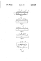
- FIGS. 1 to 4 are schematic drawings which depict the result obtained after different manufacturing steps in the process have been performed for formation of the hybrid circuit in accordance with the present invention.
- FIG. 5 is a top view of FIG. 4.
- FIG. 1 there is shown a transparent glass plate 1 having markings 3 thereon for later alignment of chips or substrates.
- the glass plate defines the planar surface which the remainder of the process will be referenced against.
- a first transparent polymer layer 5 of polymethylsiloxane having a thickness of 5 microns is then deposited over the plate 1 and a second transparent polymer layer 7 of polymethylmethacrylate having a thickness of 5 microns is deposited over the layer 5.
- the entire device of FIG. 1 is then masked to permit etching of the portion of the layer 9 which exists in the region 15 between the substrates 11 and 13.
- the region 15 is then etched away using butyl acetate followed by an oxygen plasma to remove any residues to provide the arrangement as shown in FIG. 2.
- the space 17 which now exists between the substrates 11 and 13 is then filled with an epoxy 19, such as the casting compound Emerson and Cuming Stycast 2651-40 which forms a smooth surface and degassed to provide the arrangement as shown in FIG. 3 with the epoxy layer 19.
- the epoxy layer 19 secures the substrates 11 and 13 thereto and forms the surface over which the interconnects will later be formed to form the structure as shown in FIGS. 4 and 5.
- the structure as shown in FIG. 3 is then treated with acetone to dissolve the layers 5 and 7 and the remnant of layer 9 to provide the substrates 11 and 13 with circuits formed in the downward facing faces thereof, the substrates being secured together by the epoxy 19 which provides a surface coplanar with the circuit containing surfaces of the substrates.
- This arrangement is glued with an epoxy to a brass support surface 21 which also acts as a heat sink for the hybrid circuit being formed as shown in FIG. 4. It can be seen that the circuit carrying surface of each of the substrates 11 and 13 is facing away from the support 21.
- This structure is then patterned with a photoresist in standard manner and interconnect lines 23 are formed in standard manner which extend from pads 25 on substrate 11 to pads 27 on substrate 13 as shown in FIGS. 4 and 5 to form the completed hybrid circuit.
- the hybrid circuit can then be packaged in standard manner to provide the completed usable circuit.
Landscapes
- Combinations Of Printed Boards (AREA)
Abstract
Description
Claims (16)
Priority Applications (2)
| Application Number | Priority Date | Filing Date | Title |
|---|---|---|---|
| US07/053,459 US4815208A (en) | 1987-05-22 | 1987-05-22 | Method of joining substrates for planar electrical interconnections of hybrid circuits |
| US07/470,404 US5045970A (en) | 1987-05-22 | 1990-01-26 | Joined substrates having planar electrical interconnection of hybrid circuits |
Applications Claiming Priority (1)
| Application Number | Priority Date | Filing Date | Title |
|---|---|---|---|
| US07/053,459 US4815208A (en) | 1987-05-22 | 1987-05-22 | Method of joining substrates for planar electrical interconnections of hybrid circuits |
Related Child Applications (1)
| Application Number | Title | Priority Date | Filing Date |
|---|---|---|---|
| US24870688A Division | 1987-05-22 | 1988-09-26 |
Publications (1)
| Publication Number | Publication Date |
|---|---|
| US4815208A true US4815208A (en) | 1989-03-28 |
Family
ID=21984393
Family Applications (1)
| Application Number | Title | Priority Date | Filing Date |
|---|---|---|---|
| US07/053,459 Expired - Lifetime US4815208A (en) | 1987-05-22 | 1987-05-22 | Method of joining substrates for planar electrical interconnections of hybrid circuits |
Country Status (1)
| Country | Link |
|---|---|
| US (1) | US4815208A (en) |
Cited By (3)
| Publication number | Priority date | Publication date | Assignee | Title |
|---|---|---|---|---|
| US5591678A (en) * | 1993-01-19 | 1997-01-07 | He Holdings, Inc. | Process of manufacturing a microelectric device using a removable support substrate and etch-stop |
| US6646354B2 (en) * | 1997-08-22 | 2003-11-11 | Micron Technology, Inc. | Adhesive composition and methods for use in packaging applications |
| US6699928B2 (en) | 1997-08-22 | 2004-03-02 | Micron Technology, Inc. | Adhesive composition for use in packaging applications |
Citations (10)
| Publication number | Priority date | Publication date | Assignee | Title |
|---|---|---|---|---|
| US3466741A (en) * | 1965-05-11 | 1969-09-16 | Siemens Ag | Method of producing integrated circuits and the like |
| US3501832A (en) * | 1966-02-26 | 1970-03-24 | Sony Corp | Method of making electrical wiring and wiring connections for electrical components |
| US3903590A (en) * | 1973-03-10 | 1975-09-09 | Tokyo Shibaura Electric Co | Multiple chip integrated circuits and method of manufacturing the same |
| JPS5323565A (en) * | 1976-08-17 | 1978-03-04 | Nec Corp | Production of bump semiconductor device |
| JPS5447901A (en) * | 1977-09-26 | 1979-04-16 | Babcock Hitachi Kk | Device for preventing steam generator from vibrating |
| JPS5447902A (en) * | 1977-09-26 | 1979-04-16 | Toshiba Corp | Dust protective device |
| JPS557677A (en) * | 1978-07-04 | 1980-01-19 | Japan Aviation Electronics Ind Ltd | Detection method of image sensor photo detection position |
| JPS5832425A (en) * | 1981-07-31 | 1983-02-25 | Clarion Co Ltd | Connection of circuit element |
| US4466181A (en) * | 1981-12-04 | 1984-08-21 | Clarion Co., Ltd. | Method for mounting conjoined devices |
| JPS624351A (en) * | 1985-06-29 | 1987-01-10 | Toshiba Corp | Manufacture of semiconductor carrier |
-
1987
- 1987-05-22 US US07/053,459 patent/US4815208A/en not_active Expired - Lifetime
Patent Citations (10)
| Publication number | Priority date | Publication date | Assignee | Title |
|---|---|---|---|---|
| US3466741A (en) * | 1965-05-11 | 1969-09-16 | Siemens Ag | Method of producing integrated circuits and the like |
| US3501832A (en) * | 1966-02-26 | 1970-03-24 | Sony Corp | Method of making electrical wiring and wiring connections for electrical components |
| US3903590A (en) * | 1973-03-10 | 1975-09-09 | Tokyo Shibaura Electric Co | Multiple chip integrated circuits and method of manufacturing the same |
| JPS5323565A (en) * | 1976-08-17 | 1978-03-04 | Nec Corp | Production of bump semiconductor device |
| JPS5447901A (en) * | 1977-09-26 | 1979-04-16 | Babcock Hitachi Kk | Device for preventing steam generator from vibrating |
| JPS5447902A (en) * | 1977-09-26 | 1979-04-16 | Toshiba Corp | Dust protective device |
| JPS557677A (en) * | 1978-07-04 | 1980-01-19 | Japan Aviation Electronics Ind Ltd | Detection method of image sensor photo detection position |
| JPS5832425A (en) * | 1981-07-31 | 1983-02-25 | Clarion Co Ltd | Connection of circuit element |
| US4466181A (en) * | 1981-12-04 | 1984-08-21 | Clarion Co., Ltd. | Method for mounting conjoined devices |
| JPS624351A (en) * | 1985-06-29 | 1987-01-10 | Toshiba Corp | Manufacture of semiconductor carrier |
Cited By (4)
| Publication number | Priority date | Publication date | Assignee | Title |
|---|---|---|---|---|
| US5591678A (en) * | 1993-01-19 | 1997-01-07 | He Holdings, Inc. | Process of manufacturing a microelectric device using a removable support substrate and etch-stop |
| US6646354B2 (en) * | 1997-08-22 | 2003-11-11 | Micron Technology, Inc. | Adhesive composition and methods for use in packaging applications |
| US6699928B2 (en) | 1997-08-22 | 2004-03-02 | Micron Technology, Inc. | Adhesive composition for use in packaging applications |
| US6709896B1 (en) | 1997-08-22 | 2004-03-23 | Micron Technology, Inc. | Methods for use in packaging applications using an adhesive composition |
Similar Documents
| Publication | Publication Date | Title |
|---|---|---|
| JP3986575B2 (en) | Manufacturing method of three-dimensional integrated circuit | |
| EP0099544B1 (en) | Method for forming conductive lines and via studs on lsi carrier substrates | |
| US6506664B1 (en) | Method of transferring ultra-thin substrates and application of the method to the manufacture of a multi-layer thin film device | |
| US6861345B2 (en) | Method of disposing conductive bumps onto a semiconductor device | |
| US10700034B2 (en) | Protrusion bump pads for bond-on-trace processing | |
| EP0676087B1 (en) | Fabricating stacks of ic chips by segmenting a larger stack | |
| US8409971B2 (en) | Integrated multicomponent device in a semiconducting die | |
| JP4694305B2 (en) | Manufacturing method of semiconductor wafer | |
| US8383460B1 (en) | Method for fabricating through substrate vias in semiconductor substrate | |
| JP2008521214A (en) | Thinner semiconductor wafers | |
| JP2001308095A (en) | Semiconductor device and method of manufacture | |
| US5045970A (en) | Joined substrates having planar electrical interconnection of hybrid circuits | |
| JP2597396B2 (en) | Method of forming pattern of silicone rubber film | |
| JPS61111584A (en) | Monolithic semiconductor structure and making thereof | |
| JP3523815B2 (en) | Semiconductor device | |
| US7351608B1 (en) | Method of precisely aligning components in flexible integrated circuit module | |
| JP2014033151A (en) | Manufacturing method of semiconductor device and pseudo wafer | |
| JPH11204519A (en) | Semiconductor device and manufacturing method thereof | |
| US6329302B1 (en) | Removal of a top IC die from a bottom IC die of a multichip IC package with preservation of interconnect | |
| JP2748530B2 (en) | Method for manufacturing semiconductor device | |
| US9999138B2 (en) | Making interconnections by curving conducting elements under a microelectronic device such as a chip | |
| JP2874184B2 (en) | Method for manufacturing semiconductor device | |
| JPH0521597A (en) | Method for manufacturing semiconductor device | |
| KR940007290B1 (en) | How to Form Wire Bonding Pads | |
| EP0306890A1 (en) | A semiconductor module having active devices disposed in substrate cavities |
Legal Events
| Date | Code | Title | Description |
|---|---|---|---|
| AS | Assignment |
Owner name: TEXAS INSTRUMENTS INCORPORATED, 13500 NORTH CENTRA Free format text: ASSIGNMENT OF ASSIGNORS INTEREST.;ASSIGNOR:RASCHKE, CURT R.;REEL/FRAME:004714/0786 Effective date: 19870428 Owner name: TEXAS INSTRUMENTS INCORPORATED, TEXAS Free format text: ASSIGNMENT OF ASSIGNORS INTEREST;ASSIGNOR:RASCHKE, CURT R.;REEL/FRAME:004714/0786 Effective date: 19870428 |
|
| STCF | Information on status: patent grant |
Free format text: PATENTED CASE |
|
| FEPP | Fee payment procedure |
Free format text: PAYOR NUMBER ASSIGNED (ORIGINAL EVENT CODE: ASPN); ENTITY STATUS OF PATENT OWNER: LARGE ENTITY |
|
| FPAY | Fee payment |
Year of fee payment: 4 |
|
| FPAY | Fee payment |
Year of fee payment: 8 |
|
| FPAY | Fee payment |
Year of fee payment: 12 |