US4814636A - Full pixel pulse stretching for phase reversal scophony transmission - Google Patents
Full pixel pulse stretching for phase reversal scophony transmission Download PDFInfo
- Publication number
- US4814636A US4814636A US07/130,586 US13058687A US4814636A US 4814636 A US4814636 A US 4814636A US 13058687 A US13058687 A US 13058687A US 4814636 A US4814636 A US 4814636A
- Authority
- US
- United States
- Prior art keywords
- bits
- group
- bit
- signal
- positive
- Prior art date
- Legal status (The legal status is an assumption and is not a legal conclusion. Google has not performed a legal analysis and makes no representation as to the accuracy of the status listed.)
- Expired - Lifetime
Links
Images


Classifications
-
- H—ELECTRICITY
- H03—ELECTRONIC CIRCUITRY
- H03K—PULSE TECHNIQUE
- H03K5/00—Manipulating of pulses not covered by one of the other main groups of this subclass
- H03K5/01—Shaping pulses
- H03K5/04—Shaping pulses by increasing duration; by decreasing duration
- H03K5/05—Shaping pulses by increasing duration; by decreasing duration by the use of clock signals or other time reference signals
Definitions
- FIG. 13 and accompanying text shows phase reversal being used in optical image formation. This means that for each successive group, the ON voltage will first be positive and then negative. Thus, for example, for three successive groups of ON bits, the first will be represented by a positive voltage, the second by a negative voltage and the third represented by a positive voltage. The OFF bits will always be zero volts.
- the highest primary signal frequency that can be represented by a bit stream is where single ON and OFF bits alternate.
- Using the system of phase reversal results in a reduction of the primary signal by a factor of two, but the waveform contains a high content of odd harmonics.
- each group of ON bits can be extended by one bit.
- alternating ON and OFF bits becomes a series of two positive clock periods followed by two negative clock periods.
- Groups containing two ON bits become groups of three, groups of three become groups of four, etc.
- the result of this transformation is the reduction of the harmonic content and increase of the signal component.
- the resultant three bit groups will yield about a 30% increase in the fundamental component, and about a 50% decrease in the third and fifth harmonic components, than the original bit stream would have contained.
- This invention is useful in an optical raster output scanner where a greater amount of power in the fundamental frequency and less in the higher harmonics will result in greater image intensity for the same data rate.
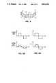
- FIG. 1a is a timing diagram of a line of typical binary bits.
- FIG. 1b is a timing diagram showing of line of FIG. 1a converted to a line of phase reversed bits.
- FIG. 2a is a timing diagram of a line of typical phase reversed bits.
- FIG. 2b is a timing diagram of a conversion of the line of FIG. 2a to a full pixel stretched line of bits.
- FIG. 3a is a simplified schematic diagram of a circuit to produce pulse stretching and phase reversal.
- FIG. 3b1 and 3b2 is a schematic diagram of the circuit for producing the pulse stretching.
- FIG. 4 is a timing diagram of the waveshapes of the circuit of FIG. 3.
- FIG. 5 is a diagram of a polygon showing the points that light generated by various harmonics will strike the polygon with respect to the current facet.
- FIG. 6a shows the filtered electrical signal and light amplitude as a product of a prior art phase reversed signal.
- FIG. 6b shows the filtered electrical signal and light amplitude as a product of a stretched and phase reversed signal.
- FIG. 1a is a diagram of a prior art binary bit stream where the first group comprises one bit, the second group comprises two bits and the third group comprises three bits, all separated by one or two zero OFF bits.
- the fundamental frequency can be reduced by using phase reversal, as shown in FIG. 1b.
- the first one-bit group is positive
- the second two-bit group is negative
- the third three-bit group is positive again
- all groups are separated by at least one zero level OFF bit.
- FIG. 2a is a timing diagram of normal phase reversal and FIG. 2b shows each group stretched by a full bit.
- FIG. 2b shows each group stretched by a full bit.
- the negative ON signal at clock period 3 of FIG. 2a has been stretched to a two bit negative signal at FIG. 2b covering clock periods 3 and 4.
- the groups having a plurality of bits are also stretched by one full bit.
- the two negative bits at clock periods 13 and 14 of FIG. 2a are stretched to three negative bits at clock periods 13, 14 and 15 of FIG. 2b
- the two positive bits at clock periods 17 and 18 of FIG. 2a are stretched to three positive bits at clock periods 17, 18 and 19 of FIG. 2b.
- FIG. 3a is a simplified diagram of one method to accomplish the pulse stretching and phase reversal functions.
- the three flip flops are of the "D" type, wherein the Q outputs reflect the D input at the negative transition of the clock input.
- the flip flop Q1 is used to restore the shape and synchronization of the incoming signal, and to provide a complementary signal for the pulse stretching and phase reversal circuits.
- the flip flop Q2 provides the pulse stretching function, and the Q3 flip flop provides the switching command for the phase reversal function.
- the appearance of the incoming signal to the circuit of FIG. 3a is as shown in FIG. 1a.
- the clock signal in conjunction with Q1, provides signals that have been phase synchronized with the clock, and have the same bit pattern as the input signal and its complement.
- the pulse stretching is accomplished by Q2, as it responds immediately to the high to low transition at the Preset input, but not to the low to high transitions at the D input.
- the signal at the D input of Q2 must remain low for two clock periods in order for this transition of Q1 to be effected.
- the complementary signal for Q1 not only presets Q2 but also toggles Q3, both events occuring at the low transition of this signal which corresponds to the low to high transition of the input signal.
- the output of Q2 is applied to one input of an electronic switch, and is also inverted and applied to the other input of the switch.
- the toggle flip flop Q3 then switches the output between the two inputs each time three is a positive transition of the input signal.
- the resultant output signal then has the apearance of the waveform shown in FIG. 2b.
- FIG. 3b1 and 3b2 is a detailed schematic diagram of a circuit for accomplishing this full bit stretching function and phase reversal.
- the normal binary input is applied to J1 at line 21, the waveshape on that line being shown in FIG. 4 as waveshape number 21.
- This is a typical binary pulse train with ON pulses at a positive voltage and OFF pulses at zero volts. These are applied to an amplifier/inverter U1 to more clearly define the leading and trailing edges of the signal and are then applied to fixed delay U3.
- This signal has to be aligned in its timing with other circuits in the system. By providing a fixed timing at this point, and variable timing at the other circuits, the system timing can be synchronized.
- the signal goes simultaneously to an OR gat U7, and another delay line U5.
- the waveshape at pin 7 and U7 is shown as waveshape 22 of FIG. 4, a negative going binary bit stream.
- the waveshape at pin 6 of U7 is shown as waveshape 23, a negative going binary bit stream delayed by one clock period.
- These are ORed at U7 to produce a bit stream at pin 3 of U7 where every group is stretched by one pulse, as shown in FIG. 4 waveshape 24. One bit is stretched to two bits, two are stretched to three, etc.
- the amount of delay of delay line U5 is the amount of time that will be added to each group of bits, and has been described throughout this description as a full pulse width. However, there is no reason why it has to be exactly one full bit, and, in fact, in this described embodiment, it is less.
- the basic clock period is fifteen nanoseconds in this described embodiment but the delay is twelve. That is to make sure that there are no glitches in the system even when imperfect circuit components may be used.
- the binary bit stream is used to modulate the optical beam, as described in the above cited article.
- the beam pattern at the polygon appears as shown in FIG. 5.
- the unmodulated main beam 52 is split into two sidebeams 51, that correspond to the fundamental frequency sidebands of the modulating signal.
- sidebeams that correspond to harmonics of this signal are also generated, four such sidebeams 53, 55 from the third and fifth harmonics being shown.
- These harmonic sidebeams will fall outside the current facet and represent lost illuminating energy. It is for this reason that it is important in an optical system that these higher frequencies be filtered out of the applied video signal so that a maximum of the applied beam falls on the current facet.
- the binary bit stream is simply electrically filtered to remove the harmonics, then the amplitude of the signal would suffer as well, and there would be essentially no difference between losing optical energy by spatial filtering (loss of sidebands at the facet) or loss of electrical amplitude by electrical filtering, as the lower electrical signal would produce less diffracted energy into the fundamental bands in either case.
- FIGS. 6a and 6b show the processed video signals, and the resultant electrical or optical amplitude, for normal video and stretched video, respectfully.
- light intensity is the square of the light amplitude, and thus a difference of 1.41 in light amplitude yields a two-to-one increase in intensity.
- the intensity of the image of a video signal of maximum pulse rate that is one ON and one OFF, can be doubled by this pulse stretching technique. This is understandable since the ON time of each pulse is also doubled.
Landscapes
- Physics & Mathematics (AREA)
- Nonlinear Science (AREA)
- Facsimile Scanning Arrangements (AREA)
- Fax Reproducing Arrangements (AREA)
- Facsimile Image Signal Circuits (AREA)
Abstract
Description
Claims (4)
Priority Applications (2)
| Application Number | Priority Date | Filing Date | Title |
|---|---|---|---|
| US07/130,586 US4814636A (en) | 1987-12-09 | 1987-12-09 | Full pixel pulse stretching for phase reversal scophony transmission |
| JP63305083A JP2621965B2 (en) | 1987-12-09 | 1988-12-01 | Method of using binary bits for photoreceptor exposure |
Applications Claiming Priority (1)
| Application Number | Priority Date | Filing Date | Title |
|---|---|---|---|
| US07/130,586 US4814636A (en) | 1987-12-09 | 1987-12-09 | Full pixel pulse stretching for phase reversal scophony transmission |
Publications (1)
| Publication Number | Publication Date |
|---|---|
| US4814636A true US4814636A (en) | 1989-03-21 |
Family
ID=22445377
Family Applications (1)
| Application Number | Title | Priority Date | Filing Date |
|---|---|---|---|
| US07/130,586 Expired - Lifetime US4814636A (en) | 1987-12-09 | 1987-12-09 | Full pixel pulse stretching for phase reversal scophony transmission |
Country Status (2)
| Country | Link |
|---|---|
| US (1) | US4814636A (en) |
| JP (1) | JP2621965B2 (en) |
Cited By (1)
| Publication number | Priority date | Publication date | Assignee | Title |
|---|---|---|---|---|
| US5196949A (en) * | 1990-10-10 | 1993-03-23 | Xerox Corporation | Vestigial sideband scophony imaging modulator |
Families Citing this family (2)
| Publication number | Priority date | Publication date | Assignee | Title |
|---|---|---|---|---|
| JP4360424B2 (en) | 2007-06-06 | 2009-11-11 | ブラザー工業株式会社 | Driving force transmission mechanism, image forming apparatus and method of assembling the same |
| JP2010084881A (en) | 2008-10-01 | 2010-04-15 | Kyocera Mita Corp | Drive transmission device and image forming apparatus including the same |
Citations (9)
| Publication number | Priority date | Publication date | Assignee | Title |
|---|---|---|---|---|
| US3278898A (en) * | 1962-12-31 | 1966-10-11 | Ibm | Data transmission system for distinctively modulating given datum bits for parity checking |
| US3424989A (en) * | 1964-05-19 | 1969-01-28 | Tideland Signal Corp | Circuit for conserving battery power by eliminating the third harmonic of an electrical square wave |
| US4213158A (en) * | 1978-06-28 | 1980-07-15 | Xerox Corporation | Optical data recording system utilizing acoustic pulse imaging to minimize image blur |
| US4253725A (en) * | 1979-04-05 | 1981-03-03 | Xerox Corporation | Single sideband scanner |
| JPS5744327A (en) * | 1980-08-29 | 1982-03-12 | Anritsu Corp | Pulse increasing circuit for clock pulse signal |
| JPS5744326A (en) * | 1980-08-29 | 1982-03-12 | Anritsu Corp | Pulse removing circuit for clock pulse signal |
| US4357627A (en) * | 1980-04-28 | 1982-11-02 | Xerox Corporation | Method and apparatus for improving resolution of scophony scanning system utilizing carrier phase reversal |
| US4397042A (en) * | 1981-07-22 | 1983-08-02 | Sumitomo Electric Industries, Ltd. | Optical modulation/demodulation system |
| US4639073A (en) * | 1984-03-19 | 1987-01-27 | Xerox Corporation | Electro-optic pulse imaging raster output scanner |
Family Cites Families (2)
| Publication number | Priority date | Publication date | Assignee | Title |
|---|---|---|---|---|
| JPS488107U (en) * | 1971-06-10 | 1973-01-29 | ||
| JPS5412612A (en) * | 1977-06-30 | 1979-01-30 | Nippon Telegr & Teleph Corp <Ntt> | Signal processing system |
-
1987
- 1987-12-09 US US07/130,586 patent/US4814636A/en not_active Expired - Lifetime
-
1988
- 1988-12-01 JP JP63305083A patent/JP2621965B2/en not_active Expired - Fee Related
Patent Citations (9)
| Publication number | Priority date | Publication date | Assignee | Title |
|---|---|---|---|---|
| US3278898A (en) * | 1962-12-31 | 1966-10-11 | Ibm | Data transmission system for distinctively modulating given datum bits for parity checking |
| US3424989A (en) * | 1964-05-19 | 1969-01-28 | Tideland Signal Corp | Circuit for conserving battery power by eliminating the third harmonic of an electrical square wave |
| US4213158A (en) * | 1978-06-28 | 1980-07-15 | Xerox Corporation | Optical data recording system utilizing acoustic pulse imaging to minimize image blur |
| US4253725A (en) * | 1979-04-05 | 1981-03-03 | Xerox Corporation | Single sideband scanner |
| US4357627A (en) * | 1980-04-28 | 1982-11-02 | Xerox Corporation | Method and apparatus for improving resolution of scophony scanning system utilizing carrier phase reversal |
| JPS5744327A (en) * | 1980-08-29 | 1982-03-12 | Anritsu Corp | Pulse increasing circuit for clock pulse signal |
| JPS5744326A (en) * | 1980-08-29 | 1982-03-12 | Anritsu Corp | Pulse removing circuit for clock pulse signal |
| US4397042A (en) * | 1981-07-22 | 1983-08-02 | Sumitomo Electric Industries, Ltd. | Optical modulation/demodulation system |
| US4639073A (en) * | 1984-03-19 | 1987-01-27 | Xerox Corporation | Electro-optic pulse imaging raster output scanner |
Non-Patent Citations (2)
| Title |
|---|
| Johnson et al., "Scophony Spatial Light Modulator", Optical Engineering--vol. 24, No. 1--Jan./Feb. 1985--pp. 93-100. |
| Johnson et al., Scophony Spatial Light Modulator , Optical Engineering vol. 24, No. 1 Jan./Feb. 1985 pp. 93 100. * |
Cited By (1)
| Publication number | Priority date | Publication date | Assignee | Title |
|---|---|---|---|---|
| US5196949A (en) * | 1990-10-10 | 1993-03-23 | Xerox Corporation | Vestigial sideband scophony imaging modulator |
Also Published As
| Publication number | Publication date |
|---|---|
| JPH02140059A (en) | 1990-05-29 |
| JP2621965B2 (en) | 1997-06-18 |
Similar Documents
| Publication | Publication Date | Title |
|---|---|---|
| US4339724A (en) | Filter | |
| US4334237A (en) | Adaptive amplitude averaging for weighting quantizing noise | |
| US4855894A (en) | Frequency converting apparatus | |
| JP2532399B2 (en) | Image processing device | |
| EP0212990B1 (en) | Image processing apparatus | |
| US5243346A (en) | Digital-to-analog converting device using decoders and parallel-to-serial converters | |
| KR910010931A (en) | Receiver Quadrature Sampling Input Signals Directly | |
| US4368439A (en) | Frequency shift keying system | |
| US4814636A (en) | Full pixel pulse stretching for phase reversal scophony transmission | |
| US4212008A (en) | Circuit for displaying characters on limited bandwidth, raster scanned display | |
| WO2001067607B1 (en) | Dynamic phase logic gate | |
| US4727361A (en) | Digital video encoder circuit | |
| US3594509A (en) | Delta modulator apparatus | |
| JPS6358584A (en) | Image processing device | |
| EP0306760B1 (en) | Coherent digital signal blanking, biphase modulation and frequency doubling circuit and methodology | |
| JPS5817778A (en) | Binary coding system | |
| JPS5821979B2 (en) | Image signal halftone processing method | |
| JPS6133078A (en) | Contour correction circuit | |
| JPS58137341A (en) | Pulse code modulation system | |
| SU1113822A2 (en) | Device for determining coordinates of point light objects | |
| JP2974318B2 (en) | Image processing device | |
| JPS58197961A (en) | Picture signal processing method | |
| SU571896A1 (en) | Analogue-digital converter | |
| SU766040A1 (en) | Signal decoder | |
| GB1437429A (en) | Generation of hadamard transforms of electrical signals |
Legal Events
| Date | Code | Title | Description |
|---|---|---|---|
| AS | Assignment |
Owner name: XEROX CORPORATION, STAMFORD, CONNECTICUT A CORP. O Free format text: ASSIGNMENT OF ASSIGNORS INTEREST.;ASSIGNOR:SWANBERG, MELVIN E.;REEL/FRAME:004799/0853 Effective date: 19871204 Owner name: XEROX CORPORATION, STAMFORD, CONNECTICUT A CORP. O Free format text: ASSIGNMENT OF ASSIGNORS INTEREST;ASSIGNOR:SWANBERG, MELVIN E.;REEL/FRAME:004799/0853 Effective date: 19871204 |
|
| STCF | Information on status: patent grant |
Free format text: PATENTED CASE |
|
| FEPP | Fee payment procedure |
Free format text: PAYOR NUMBER ASSIGNED (ORIGINAL EVENT CODE: ASPN); ENTITY STATUS OF PATENT OWNER: LARGE ENTITY |
|
| FPAY | Fee payment |
Year of fee payment: 4 |
|
| FPAY | Fee payment |
Year of fee payment: 8 |
|
| FPAY | Fee payment |
Year of fee payment: 12 |
|
| AS | Assignment |
Owner name: BANK ONE, NA, AS ADMINISTRATIVE AGENT, ILLINOIS Free format text: SECURITY INTEREST;ASSIGNOR:XEROX CORPORATION;REEL/FRAME:013153/0001 Effective date: 20020621 |
|
| AS | Assignment |
Owner name: JPMORGAN CHASE BANK, AS COLLATERAL AGENT, TEXAS Free format text: SECURITY AGREEMENT;ASSIGNOR:XEROX CORPORATION;REEL/FRAME:015134/0476 Effective date: 20030625 Owner name: JPMORGAN CHASE BANK, AS COLLATERAL AGENT,TEXAS Free format text: SECURITY AGREEMENT;ASSIGNOR:XEROX CORPORATION;REEL/FRAME:015134/0476 Effective date: 20030625 |
|
| AS | Assignment |
Owner name: XEROX CORPORATION, CONNECTICUT Free format text: RELEASE BY SECURED PARTY;ASSIGNOR:JPMORGAN CHASE BANK, N.A. AS SUCCESSOR-IN-INTEREST ADMINISTRATIVE AGENT AND COLLATERAL AGENT TO JPMORGAN CHASE BANK;REEL/FRAME:066728/0193 Effective date: 20220822 |