US4806889A - Ceramic filter - Google Patents
Ceramic filter Download PDFInfo
- Publication number
- US4806889A US4806889A US07/187,430 US18743088A US4806889A US 4806889 A US4806889 A US 4806889A US 18743088 A US18743088 A US 18743088A US 4806889 A US4806889 A US 4806889A
- Authority
- US
- United States
- Prior art keywords
- slits
- ceramic body
- accordance
- depth
- dielectric ceramic
- Prior art date
- Legal status (The legal status is an assumption and is not a legal conclusion. Google has not performed a legal analysis and makes no representation as to the accuracy of the status listed.)
- Expired - Lifetime
Links
Images


Classifications
-
- H—ELECTRICITY
- H01—ELECTRIC ELEMENTS
- H01P—WAVEGUIDES; RESONATORS, LINES, OR OTHER DEVICES OF THE WAVEGUIDE TYPE
- H01P1/00—Auxiliary devices
- H01P1/20—Frequency-selective devices, e.g. filters
- H01P1/201—Filters for transverse electromagnetic waves
- H01P1/205—Comb or interdigital filters; Cascaded coaxial cavities
- H01P1/2056—Comb filters or interdigital filters with metallised resonator holes in a dielectric block
Definitions
- the present invention relates to a dielectric ceramic body which is adapted to be used for a ceramic bandpass filter. More particularly, the present invention pertains to a dielectric ceramic body of a substantially cuboidal configuration having a conductive or short-circuited surface which is coated with a layer of a conductive material and an open surface which is opposite to the conductive surface and is not coated with a conductive material, one of the conductive and open surfaces being formed with a plurality of spaced apart slits which determine coupling properties in the body.
- a ceramic filter has been structured to include a plurality of cylindrical ceramic bodies which are arranged in series and electrically connected to provide a transmitter resonator and a receiver resonator, respectively.
- This type of ceramic filter is disclosed for example by the U.S. Pat. No. 4,255,729 issued to A. Fukasawa et. al. on Mar. 10, 1981.
- the known type of ceramic filter is found disadvantageous in that it requires a lot of labors in manufacture.
- the U.S. Pat. No. 3,505,618 issued to F. B. L McKee on Apr. 7, 1970 discloses a filter which is made of a dielectric body of a substantially cuboidal configuration.
- the body is formed with a plurality of through holes which are arranged in series and extend from one surface of the body to the opposite surface.
- the body is covered by a layer of a conductive material such as silver.
- the holes have surfaces which are covered by a conductive material and conductive terminals may be inserted into selected holes to provide an input and an output.
- the body may be made of a dielectric ceramic material as disclosed by the U.S. Pat. No. 4,464,640 issued to T. Nishikawa et. al. on Aug. 7, 1984.
- the ceramic body is covered by a conductive material except a surface where one ends of the holes are opened.
- the surface which is not covered by the conductive material may be referred as the open surface and the surface which is covered by the conductive material and opposite to the open surface may be referred as the short-circuited surface.
- a slit is formed between the holes. As shown in the U.S. Pat.
- the ceramic body may be of an elongated configuration and a plurality of holes may be formed and arranged in series in the axial direction of the body.
- a slit is formed between each two adjacent pair of the holes.
- This type of ceramic filters are useful in that it can be readily assembled and less expensively manufactured.
- the number of the holes may be appropriately determined to obtain a desired function.
- a desired resonating frequency is obtained through an adjustment of the volume of the dielectric material between the conductive layers on the surfaces of each two adjacent holes or the conductive layer on the surface of each hole and the outer surface of the ceramic body.
- the thickness of the ceramic body or the distance between the open surface and the short-circuited surface is appropriately changed to thereby change the lengths of the holes.
- the thickness of the ceramic body may be reduced to provide a shortened hole length or a piece of dielectric material may be added to an appropriate portion of the ceramic body.
- Another object of the present invention is to provide a ceramic filter having a dielectric ceramic body formed with a plurality of through holes extending from one surface to another surface opposite to the one surface and a slit formed in one of the said surfaces between two adjacent holes, the filter having a versatility in obtaining a desired property.
- a dielectric ceramic body for a ceramic filter said body being of a cuboidal configuration having first side surface and a second side surface which is opposite to said first side surface, a plurality of holes arranged in series along a length of said body to extend from said first side surface to said second side surface and opening at the opposite ends to said first and second side surfaces, a plurality of slits formed at one of said first and second side surfaces and located one between each two adjacent pair of said holes, a first conductive layer provided at least on one of said first and second surfaces, a second conductive layer provided on an interior wall of each hole, said slits having depths which change so that the depth of the slit at an end portion of the ceramic body is greater than the depth of the slit at an intermediate portion of the ceramic body.
- the ceramic body may be an elongated cuboidal configuration having opposite end portions with the first and second side surfaces extending between said end portions, at least a predetermined number of slits from each end having lengths which increase toward said end portion of the ceramic body so that bottom portion of the slits are located substantially along a parabolic curve.
- the ceramic body has five holes, there are formed three slits in the body. The slits at the opposite end portions then have depths which are greater than the depth of the central slit.
- the central two slits may have substantilly the same depth and the outer two slits may have depths which are greater than the depths of the central slits.
- the depths of the slits are increased toward each end so that the bottoms of the slits are located along a elliptic or parabolic curve.
- at least three slits from each end are increased in depth toward the end of the body and the remaining slits may have substantially the same depths or the depths of the remaining slits may be increased gradually toward each end.
- the ceramic body for the filter is required to have a stronger coupling at the hole located at an axially outer portion than at the hole located at an axially inner portion of the body
- the slit depths described above provide desirable property to meet the above requirement.
- the increase in the depths of the slits toward each end of the body provides a versatility in obtaining a desired coupling property at each hole of the ceramic filter.
- It is preferable that the slit depth change is substantially symmetrical with respect to the axial center of the ceramic body.
- the ceramic body may have a decreased thickness at each end for the convenience of attaching a terminal.
- FIG. 1 is a side view of a dielectric ceramic body in accordance with one embodiment of the present invention
- FIG. 2 is a side view similar to FIG. 1 but showing a modified form
- FIGS. 3 and 4 are side views showing further modifications
- FIG. 5 is a side view showing a dielectric ceramic body having slits in the short-circuited surface
- FIG. 6 is a side view showing a modification of the ceramic body shown in FIG. 5;
- FIGS. 7 and 8 are side views showing further modifications
- FIGS. 9 and 10 are diagrammatical illustrations of ceramic bodies having three slits
- FIGS. 11 and 12 are diagrammatical illustrations of ceramic bodies having four slits
- FIGS. 13 and 14 are diagrammatical illustrations of ceramic bodies having more than six slits
- FIG. 15 is a perspective view of a ceramic body showing a manner of adjusting the resonant frequency of each resonator of the filter;
- FIGS. 16, 17 and 18 are fragmentary plan views showing manners of adjusting the resonant frequency of each resonator of the filter
- FIG. 19 is a fragmentary sectional view taken along the line A 1 --A 1 in FIG. 18 to show the manner of adjusting the resonant frequency;
- FIG. 20 is a fragmentary plan view showing a further manner of adjusting the resonant frequency
- FIG. 21 is a sectional view taken along the line A 2 --A 2 in FIG. 20;
- FIGS. 22 and 23 are fragmentary plan view showing further different manners of adjusting the resonant frequency
- FIG. 24 is a diagram showing the result of resonant frequency adjustment in accordance with the present invention.
- FIG. 25 is a diagram showing the relationship between the spacings of the holes and the depths of the slits.
- FIG. 26 is a diagram showing the effect of the conductive coating in the slit.
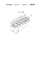
- a dielectric ceramic body 1 of a substantially cuboidal configuration having four side surfaces 1a, 1b, 1c and 1d and two end surfaces 1e and 1f.
- the ceramic body 1 is formed with six through holes 21, 22, 23, 24, 25 and 26 which extend from the top or side surface 1a to the bottom or side surface 1c and arranged in series in the axial direction of the body as shown by an arrow X in FIG. 15.
- the ceramic body 1 is further formed at the top surface 1a with slits 41, 42, 43, 44 and 45 which are located between respective pairs of the holes 21, 22, 23, 24, 25 and 26. Each of the slits extends in the transverse direction or the direction shown by an arrow Y in FIG. 15.
- the ceramic body is covered at the side surfaces 1b, 1c and 1d and the end surfaces 1e and 1f with an electrically conductive material such as silver which thus provides a conductive layer 3.
- an electrically conductive material such as silver which thus provides a conductive layer 3.
- Each of the holes 21, 22, 23, 24, 25 and 26 is also coated by a layer 3 of a conductive material such as silver.
- the side or top surface 1a is left uncoated so that the surface 1a provides an open surface.
- the side or bottom surface 1c provides a short-circuited surface.
- the holes 21, 22, 23, 24, 25 and 16 respectively provide resonating stages Q 1 , Q 2 , Q 3 , Q 4 , Q 5 and Q 6 of a ceramic filter which is obtained from the ceramic body 1.
- the slits 41 and 45 which are located at the axially outermost positions have the same depth B 1 whereas the slits 42 and 44 which are second from the axial end have the same depth B 2 .
- the axially central slit 43 has a depth B 3 which is smaller than the depths B 1 and B 2 .
- the depth B 2 for the slits 42 and 44 and the depth B 3 for the slit 43 are determined in relation to the depth B 1 for the axially outermost slits 41 and 45 by the formula
- k is a proportional coefficient having a value between 0.65 and 0.95.
- FIG. 2 shows another example of the ceramic body 1.
- the slits 41, 42, 43, 44, 45 and 46 have walls which are coated with a layer 3 of a conductive material such as silver.
- the depths of the slits 41, 42, 43, 44, 45 and 46 are determined in the same manner as in the previous example.
- the configuration of the ceramic body 1 in the examples shown in FIGS. 1 and 2 is such that the thickness of the body 1 is reduced at portions axially outside the outermost slits 41 and 45 by forming stepped portions on the top surface 1a.
- FIG. 3 shows an example in which the ceramic body 1 is different from the ceramic body 1 of the example shown in FIG. 1 in that the body 1 in FIG.
- the ceramic body 1 shown in FIG. 4 is different from the body 1 shown in FIG. 2 in that the body 1 in FIG. 4 has stepped portions on the bottom surface 1c to provide the portions of reduced thickness.
- the depths of the slits 41, 42, 43, 44, 45 and 46 are determined in the same manner as in the examples of FIGS. 1 and 2.
- FIGS. 5 through 8 show examples which correspond respectively to the examples shown in FIGS. 1 through 4.
- the examples in FIGS. 5 through 8 are different from the examples in FIGS. 1 through 4 in that the slits 41, 42, 43, 44, 45 and 46 are formed not in the top surface 1a but in the bottom surface 1c.
- the depths of the slits 41, 42, 43, 44, 45 and 46 are determined as in the examples in FIGS. 1 through 4.
- a dielectric ceramic body 11 which has four through holes 21, 22, 23 and 24 arranged in series in the axial direction of the body and extending from the top surface 11a to the bottom surface 11c.
- the body 11 is coated with a layer of a conductive material on the external surfaces except the top surface 11a. Further, the inside wall surfaces of the holes 21 through 24 are also coated with a layer of a conductive material.
- the ceramic body 11 has three slits 41, 42 and 43 which are located respectively between the holes 21, 22, 23 and 24.
- the slits 41 and 43 have substantially the same depth B 1 and the slit 42 has a depth B 2 which is smaller than the depth B 1 .
- the depth B 2 is determined in accordance with the formula
- k is a constant having a value between 0.65 and 0.95.
- FIG. 10 shows a further example of the dielectric ceramic body 11 which is substantially identical with the body 11 shown in FIG. 9.
- the slits 41, 42 and 43 are formed in the short-circuited surface 11c.
- the depths of the slits 41, 42 and 43 are determined in the same manner as in the example shown in FIG. 9.
- FIG. 11 shows a dielectric ceramic body 31 having a top surface 31a and a bottom surface 31c.
- Through holes 21, 22, 23, 24 and 25 are formed to extend from the top surface 31a to the bottom surface 31c and arranged in series in the axial direction of the body 31.
- the outer surface of the ceramic body 31 is coated with a layer of an electrically conductive material.
- the inside walls of the holes 21, 22, 23, 24 and 25 are also coated with a layer of a conductive material.
- Four slits 41, 42, 43 and 44 are formed in the top surface 31a and located respectively between adjacent pairs of the holes 21, 22, 23, 24 and 25.
- the axially outer slits 41 and 44 have substantially the same depth B 1 and the inner slits 42 and 43 have substantially the same depth B 2 which is smaller than the depths B 1 of the outer slits 41 and 44.
- the depth B 2 is determined in accordance with the formula
- k is a constant having a value between 0.65 and 0.95.
- FIG. 12 shows another example of the ceramic body 31 which is different from the ceramic body in FIG. 11 in that the slits 41 through 44 are formed in the coductively coated or short-circuited surface 31c.
- the depths of the slits 41 through 44 are determined substantially in the same manner as in the example of FIG. 11.
- the slits have depths which are so determined that the bottom portions of the slits are arranged substantially along an elliptical curve.
- FIG. 13 shows a further embodiment of the present invention in which the ceramic body 51 has top surface 51a and a bottom surface 51c and formed with holes extending from the top surface 51a to the bottom surface 51c.
- the number of the holes is N so that the holes are designated from one axial end of the body by the reference characters b 1 , b 2 , b 3 . . . b n-2 , b n-1 and b n .
- the holes have inside walls which are coated with layers of a conductive material.
- the ceramic body 51 is formed at the top surface 51a with slits s 1 , s 2 , s 3 . . . s -3 , s n-2 and s n-1 which are located between respective adjacent pairs of the holes.
- the slits S 1 , s 2 , s 3 . . . s N-3 , s N-2 and s N-1 respectively have depths B 1 , B 2 , B 3 . . . B N-3 , B N-2 and B N-1 which are determined in accordance with the formula
- m is a largest integer which does not exceed (N-1)/2 and k m is a proportional coefficient which has a value between 0.65 and 0.95 in case where m is 2 and N-1 and a value between 0.8 and 1.0 in case where m is 3 to N-2.
- the value 0.8 is adopted to determine the depth of the slit s 3 or s N-3 . Then, at least three slits from the axially outer end have depths which change so that the bottom portions of the slits are laid substantially along a parabolic curve.
- FIG. 14 shows a further example which is similar to the example shown in FIG. 13 but has slits s 1 through s N-1 formed in the short-circuited surface 51c.
- the depths of the slits s 1 through s N-1 are determined as in the example shown in FIG. 13. Where the surface having the slits is formed with stepped portions, the depth of the slit is measured from the highest part of the surface adjacent to the slit.
- the manner of determining the depths of the slits is based on the assumption that the holes have the same diameter and arranged with the same spacings. In case where the spacings between respective adjacent pairs of holes are not uniform, the slit depths must be modified. In case where the hole spacing is decreased with the same hole diameter, the coupling becomes stronger. For example, where the spacing between the holes b 1 and b 2 and the spacing between the holes b N-1 and b N are smaller than the other spacings in the embodiment of FIG. 13, the coupling at the end portions will become stronger if the depths of the slits s 1 and s N-1 are unchanged. Therefore, the slit depths must be modified in accordance with the relationship as shown in FIG. 25. As an example, as shown in FIG. 25, where the hole spacing is decreased to 83% of the standard spacing, the slit depth should be decreased to 66% of the standard depth which is the depth of the slit required for obtaining the desired coupling with the standard hole spacing.
- FIG. 26 shows the relationship between the relative value of the inter-stage coupling and the depth of the slit with and without the conductive coating.
- the depth of the slit is designated as a ratio of the depth d and the thickness 1 of the ceramic body.
- the slit depth may be modified in accordance with the relationship as shown in FIG. 26.
- the slit depth must be 33% if the slit does not have a conductive coating, but the slit depth can be as small as 8% where the slit has a conductive coating.
- FIG. 15 there is shown regions which are used for an adjustment of the resonating frequency.
- shadowed areas which are encircled by transverse tangential lines y 1 of the holes are the adjustment regions a.
- the coupling electric field E is strongest in the axial direction X of the ceramic body along which the holes are arranged and the field is decreased toward the transverse direction Y.
- the adjustment region a is defined by the transverse tangential lines y 1 drawn at the opposite sides of the hole.
- the adjustment region is defined by a single transverse tangential line y 1 of the hole drawn at the axially inner side of the ceramic body. It is understood that the coupling electric field is curved in the transverse direction as shown by lines a 1 in FIGS. 16 and 17, however, in actual practice, the adjustment region can conveniently be defined by the straight lines y 1 .
- the dielectric material in the adjustment region a is appropriately removed for example by forming a chamfered configuration c as shown in FIGS. 18 and 19.
- the dielectric material may be removed by forming a groove g as shown in FIGS. 20 and 21.
- circular recesses r may be formed in the adjustment region a as shown in FIG. 22.
- the chamfered portion may be formed as shown in FIG. 23 at the axially outer side of the hole.
Abstract
Description
B.sub.2 =k×B.sub.1, B.sub.3 =k×B.sub.2
B.sub.2 =k×B.sub.1
B.sub.2 =k×B.sub.1
B.sub.m (or B.sub.N-m)=k.sub.m ×B.sub.m-1
Claims (15)
B.sub.2 =k×B.sub.1, B.sub.3 =k×B.sub.2
B.sub.m (or B.sub.N-m)=k.sub.m ×B.sub.m-1
Applications Claiming Priority (2)
| Application Number | Priority Date | Filing Date | Title |
|---|---|---|---|
| JP62-336653 | 1987-12-28 | ||
| JP62336653A JPH01175301A (en) | 1987-12-28 | 1987-12-28 | Dielectric filter |
Publications (1)
| Publication Number | Publication Date |
|---|---|
| US4806889A true US4806889A (en) | 1989-02-21 |
Family
ID=18301394
Family Applications (1)
| Application Number | Title | Priority Date | Filing Date |
|---|---|---|---|
| US07/187,430 Expired - Lifetime US4806889A (en) | 1987-12-28 | 1988-04-28 | Ceramic filter |
Country Status (4)
| Country | Link |
|---|---|
| US (1) | US4806889A (en) |
| EP (1) | EP0322993B1 (en) |
| JP (1) | JPH01175301A (en) |
| DE (1) | DE3850646T2 (en) |
Cited By (25)
| Publication number | Priority date | Publication date | Assignee | Title |
|---|---|---|---|---|
| US5004992A (en) * | 1990-05-25 | 1991-04-02 | Motorola, Inc. | Multi-resonator ceramic filter and method for tuning and adjusting the resonators thereof |
| US5109207A (en) * | 1989-12-19 | 1992-04-28 | Matsushita Electric Industrial Co., Ltd. | Coaxial dielectric resonator having a groove therein and method of producing such coaxial dielectric resonator |
| US5254962A (en) * | 1992-06-19 | 1993-10-19 | Motorola, Inc. | Combined acoustic wave device and ceramic block filter structure |
| US5327108A (en) * | 1991-03-12 | 1994-07-05 | Motorola, Inc. | Surface mountable interdigital block filter having zero(s) in transfer function |
| WO1995009451A1 (en) * | 1993-09-29 | 1995-04-06 | Motorola Inc. | Multi-filter device and method of making same |
| US5602518A (en) * | 1995-03-24 | 1997-02-11 | Motorola, Inc. | Ceramic filter with channeled features to control magnetic coupling |
| US5926078A (en) * | 1995-08-04 | 1999-07-20 | Ngk Spark Plug Co., Ltd. | Dielectric filter including various means of adjusting the coupling between resonators |
| US5999070A (en) * | 1996-03-15 | 1999-12-07 | Tdk Corporation | Dielectric filter having tunable resonating portions |
| US6023208A (en) * | 1995-12-12 | 2000-02-08 | Murata Manufacturing Co., Ltd. | Dielectric filter |
| US6232780B1 (en) * | 1991-03-01 | 2001-05-15 | Digital Control Incorporated | Underground locating using a locating signal transmitter configured with a single antenna |
| US6351198B1 (en) * | 1998-11-25 | 2002-02-26 | Murata Manufacturing Co., Ltd. | Dielectric filter, duplexer, and communication apparatus |
| US20140077900A1 (en) * | 2011-05-09 | 2014-03-20 | Cts Corporation | Dielectric Waveguide Filter with Direct Coupling and Alternative Cross-Coupling |
| US8823470B2 (en) | 2010-05-17 | 2014-09-02 | Cts Corporation | Dielectric waveguide filter with structure and method for adjusting bandwidth |
| US9030279B2 (en) | 2011-05-09 | 2015-05-12 | Cts Corporation | Dielectric waveguide filter with direct coupling and alternative cross-coupling |
| US9030278B2 (en) | 2011-05-09 | 2015-05-12 | Cts Corporation | Tuned dielectric waveguide filter and method of tuning the same |
| US9130258B2 (en) | 2013-09-23 | 2015-09-08 | Cts Corporation | Dielectric waveguide filter with direct coupling and alternative cross-coupling |
| US9130256B2 (en) | 2011-05-09 | 2015-09-08 | Cts Corporation | Dielectric waveguide filter with direct coupling and alternative cross-coupling |
| US9466864B2 (en) | 2014-04-10 | 2016-10-11 | Cts Corporation | RF duplexer filter module with waveguide filter assembly |
| US9583805B2 (en) | 2011-12-03 | 2017-02-28 | Cts Corporation | RF filter assembly with mounting pins |
| US9666921B2 (en) | 2011-12-03 | 2017-05-30 | Cts Corporation | Dielectric waveguide filter with cross-coupling RF signal transmission structure |
| US10050321B2 (en) | 2011-12-03 | 2018-08-14 | Cts Corporation | Dielectric waveguide filter with direct coupling and alternative cross-coupling |
| US10116028B2 (en) | 2011-12-03 | 2018-10-30 | Cts Corporation | RF dielectric waveguide duplexer filter module |
| US10483608B2 (en) | 2015-04-09 | 2019-11-19 | Cts Corporation | RF dielectric waveguide duplexer filter module |
| US11081769B2 (en) | 2015-04-09 | 2021-08-03 | Cts Corporation | RF dielectric waveguide duplexer filter module |
| US11437691B2 (en) | 2019-06-26 | 2022-09-06 | Cts Corporation | Dielectric waveguide filter with trap resonator |
Families Citing this family (2)
| Publication number | Priority date | Publication date | Assignee | Title |
|---|---|---|---|---|
| JP2561775B2 (en) * | 1991-03-29 | 1996-12-11 | 日本碍子株式会社 | Dielectric filter and method of adjusting frequency characteristics thereof |
| CN100462706C (en) * | 2005-01-06 | 2009-02-18 | 清华大学 | Standard leak |
Citations (11)
| Publication number | Priority date | Publication date | Assignee | Title |
|---|---|---|---|---|
| US3505618A (en) * | 1966-06-08 | 1970-04-07 | Marconi Co Ltd | Microwave filters |
| US4255729A (en) * | 1978-05-13 | 1981-03-10 | Oki Electric Industry Co., Ltd. | High frequency filter |
| US4431977A (en) * | 1982-02-16 | 1984-02-14 | Motorola, Inc. | Ceramic bandpass filter |
| US4464640A (en) * | 1981-10-02 | 1984-08-07 | Murata Manufacturing Co., Ltd. | Distribution constant type filter |
| JPS6143285A (en) * | 1984-08-03 | 1986-03-01 | キヤリア・コーポレイシヨン | Air-tight motor compressor having suction port and seal |
| JPS6143287A (en) * | 1984-08-03 | 1986-03-01 | Toyota Motor Corp | Operation control for compressor |
| US4607242A (en) * | 1983-05-02 | 1986-08-19 | Rockwell International Corporation | Microwave filter |
| US4692726A (en) * | 1986-07-25 | 1987-09-08 | Motorola, Inc. | Multiple resonator dielectric filter |
| JPS638642A (en) * | 1986-06-28 | 1988-01-14 | Konica Corp | Silver halide photographic sensitive material having excellent antistatic ability and antiadhesive property |
| US4733208A (en) * | 1984-08-21 | 1988-03-22 | Murata Manufacturing Co., Ltd. | Dielectric filter having impedance changing means coupling adjacent resonators |
| US4745379A (en) * | 1987-02-25 | 1988-05-17 | Rockwell International Corp. | Launcher-less and lumped capacitor-less ceramic comb-line filters |
Family Cites Families (3)
| Publication number | Priority date | Publication date | Assignee | Title |
|---|---|---|---|---|
| DE3164402D1 (en) * | 1980-04-28 | 1984-08-02 | Oki Electric Ind Co Ltd | A high frequency filter |
| GB2109641B (en) * | 1981-10-02 | 1985-08-14 | Murata Manufacturing Co | Distributed constant type filter |
| JPH06180901A (en) * | 1992-12-14 | 1994-06-28 | Sony Corp | Tape tension detector and magnetic recorder/reproducer using the same |
-
1987
- 1987-12-28 JP JP62336653A patent/JPH01175301A/en active Pending
-
1988
- 1988-04-28 US US07/187,430 patent/US4806889A/en not_active Expired - Lifetime
- 1988-05-09 EP EP88304176A patent/EP0322993B1/en not_active Expired - Lifetime
- 1988-05-09 DE DE3850646T patent/DE3850646T2/en not_active Expired - Fee Related
Patent Citations (11)
| Publication number | Priority date | Publication date | Assignee | Title |
|---|---|---|---|---|
| US3505618A (en) * | 1966-06-08 | 1970-04-07 | Marconi Co Ltd | Microwave filters |
| US4255729A (en) * | 1978-05-13 | 1981-03-10 | Oki Electric Industry Co., Ltd. | High frequency filter |
| US4464640A (en) * | 1981-10-02 | 1984-08-07 | Murata Manufacturing Co., Ltd. | Distribution constant type filter |
| US4431977A (en) * | 1982-02-16 | 1984-02-14 | Motorola, Inc. | Ceramic bandpass filter |
| US4607242A (en) * | 1983-05-02 | 1986-08-19 | Rockwell International Corporation | Microwave filter |
| JPS6143285A (en) * | 1984-08-03 | 1986-03-01 | キヤリア・コーポレイシヨン | Air-tight motor compressor having suction port and seal |
| JPS6143287A (en) * | 1984-08-03 | 1986-03-01 | Toyota Motor Corp | Operation control for compressor |
| US4733208A (en) * | 1984-08-21 | 1988-03-22 | Murata Manufacturing Co., Ltd. | Dielectric filter having impedance changing means coupling adjacent resonators |
| JPS638642A (en) * | 1986-06-28 | 1988-01-14 | Konica Corp | Silver halide photographic sensitive material having excellent antistatic ability and antiadhesive property |
| US4692726A (en) * | 1986-07-25 | 1987-09-08 | Motorola, Inc. | Multiple resonator dielectric filter |
| US4745379A (en) * | 1987-02-25 | 1988-05-17 | Rockwell International Corp. | Launcher-less and lumped capacitor-less ceramic comb-line filters |
Cited By (35)
| Publication number | Priority date | Publication date | Assignee | Title |
|---|---|---|---|---|
| US5109207A (en) * | 1989-12-19 | 1992-04-28 | Matsushita Electric Industrial Co., Ltd. | Coaxial dielectric resonator having a groove therein and method of producing such coaxial dielectric resonator |
| US5004992A (en) * | 1990-05-25 | 1991-04-02 | Motorola, Inc. | Multi-resonator ceramic filter and method for tuning and adjusting the resonators thereof |
| US6232780B1 (en) * | 1991-03-01 | 2001-05-15 | Digital Control Incorporated | Underground locating using a locating signal transmitter configured with a single antenna |
| US5327108A (en) * | 1991-03-12 | 1994-07-05 | Motorola, Inc. | Surface mountable interdigital block filter having zero(s) in transfer function |
| US5254962A (en) * | 1992-06-19 | 1993-10-19 | Motorola, Inc. | Combined acoustic wave device and ceramic block filter structure |
| WO1995009451A1 (en) * | 1993-09-29 | 1995-04-06 | Motorola Inc. | Multi-filter device and method of making same |
| US5422610A (en) * | 1993-09-29 | 1995-06-06 | Motorola, Inc. | Multi-filter device and method of making same |
| US5602518A (en) * | 1995-03-24 | 1997-02-11 | Motorola, Inc. | Ceramic filter with channeled features to control magnetic coupling |
| US5926078A (en) * | 1995-08-04 | 1999-07-20 | Ngk Spark Plug Co., Ltd. | Dielectric filter including various means of adjusting the coupling between resonators |
| CN1097861C (en) * | 1995-12-12 | 2003-01-01 | 株式会社村田制作所 | Medium wave filter |
| US6023208A (en) * | 1995-12-12 | 2000-02-08 | Murata Manufacturing Co., Ltd. | Dielectric filter |
| US5999070A (en) * | 1996-03-15 | 1999-12-07 | Tdk Corporation | Dielectric filter having tunable resonating portions |
| US6351198B1 (en) * | 1998-11-25 | 2002-02-26 | Murata Manufacturing Co., Ltd. | Dielectric filter, duplexer, and communication apparatus |
| US9130257B2 (en) * | 2010-05-17 | 2015-09-08 | Cts Corporation | Dielectric waveguide filter with structure and method for adjusting bandwidth |
| US8823470B2 (en) | 2010-05-17 | 2014-09-02 | Cts Corporation | Dielectric waveguide filter with structure and method for adjusting bandwidth |
| US20140361853A1 (en) * | 2010-05-17 | 2014-12-11 | Cts Corporation | Dielectric Waveguide Filter with Structure and Method for Adjusting Bandwidth |
| US9030279B2 (en) | 2011-05-09 | 2015-05-12 | Cts Corporation | Dielectric waveguide filter with direct coupling and alternative cross-coupling |
| US9431690B2 (en) | 2011-05-09 | 2016-08-30 | Cts Corporation | Dielectric waveguide filter with direct coupling and alternative cross-coupling |
| US20140077900A1 (en) * | 2011-05-09 | 2014-03-20 | Cts Corporation | Dielectric Waveguide Filter with Direct Coupling and Alternative Cross-Coupling |
| US9030278B2 (en) | 2011-05-09 | 2015-05-12 | Cts Corporation | Tuned dielectric waveguide filter and method of tuning the same |
| US9130256B2 (en) | 2011-05-09 | 2015-09-08 | Cts Corporation | Dielectric waveguide filter with direct coupling and alternative cross-coupling |
| US9130255B2 (en) * | 2011-05-09 | 2015-09-08 | Cts Corporation | Dielectric waveguide filter with direct coupling and alternative cross-coupling |
| US9437908B2 (en) | 2011-07-18 | 2016-09-06 | Cts Corporation | Dielectric waveguide filter with direct coupling and alternative cross-coupling |
| US9583805B2 (en) | 2011-12-03 | 2017-02-28 | Cts Corporation | RF filter assembly with mounting pins |
| US9666921B2 (en) | 2011-12-03 | 2017-05-30 | Cts Corporation | Dielectric waveguide filter with cross-coupling RF signal transmission structure |
| US10050321B2 (en) | 2011-12-03 | 2018-08-14 | Cts Corporation | Dielectric waveguide filter with direct coupling and alternative cross-coupling |
| US10116028B2 (en) | 2011-12-03 | 2018-10-30 | Cts Corporation | RF dielectric waveguide duplexer filter module |
| CN105637701A (en) * | 2013-09-23 | 2016-06-01 | Cts公司 | Dielectric waveguide filter with direct coupling and alternative cross-coupling |
| US9437909B2 (en) | 2013-09-23 | 2016-09-06 | Cts Corporation | Dielectric waveguide filter with direct coupling and alternative cross-coupling |
| US9130258B2 (en) | 2013-09-23 | 2015-09-08 | Cts Corporation | Dielectric waveguide filter with direct coupling and alternative cross-coupling |
| CN105637701B (en) * | 2013-09-23 | 2019-06-07 | Cts公司 | With direct-coupling and substitute cross-linked dielectric waveguide filter |
| US9466864B2 (en) | 2014-04-10 | 2016-10-11 | Cts Corporation | RF duplexer filter module with waveguide filter assembly |
| US10483608B2 (en) | 2015-04-09 | 2019-11-19 | Cts Corporation | RF dielectric waveguide duplexer filter module |
| US11081769B2 (en) | 2015-04-09 | 2021-08-03 | Cts Corporation | RF dielectric waveguide duplexer filter module |
| US11437691B2 (en) | 2019-06-26 | 2022-09-06 | Cts Corporation | Dielectric waveguide filter with trap resonator |
Also Published As
| Publication number | Publication date |
|---|---|
| DE3850646T2 (en) | 1994-10-27 |
| JPH01175301A (en) | 1989-07-11 |
| EP0322993A2 (en) | 1989-07-05 |
| EP0322993B1 (en) | 1994-07-13 |
| EP0322993A3 (en) | 1990-04-04 |
| DE3850646D1 (en) | 1994-08-18 |
Similar Documents
| Publication | Publication Date | Title |
|---|---|---|
| US4806889A (en) | Ceramic filter | |
| US4477785A (en) | Generalized dielectric resonator filter | |
| US5389903A (en) | Comb-line high-frequency band-pass filter having adjustment for varying coupling type between adjacent coaxial resonators | |
| JP2609427B2 (en) | Cascaded cavity with temperature compensation | |
| US4143344A (en) | Microwave band-pass filter provided with dielectric resonator | |
| US4849722A (en) | Adjustable band suspended substrate filter | |
| US5684438A (en) | Microwave filter including a plurality of cross-coupled dielectric resonators | |
| US5192926A (en) | Dielectric filter with attenuation poles | |
| US5014024A (en) | Bandpass filter and method of trimming response characteristics thereof | |
| JPS63220603A (en) | Ceramic waveguide filtering circuit | |
| US6876277B2 (en) | E-plane filter and a method of forming an E-plane filter | |
| US3680012A (en) | Microwave band-pass filter having constant bandwidth as filter is tuned | |
| JPH0369202B2 (en) | ||
| US5004993A (en) | Constricted split block waveguide low pass filter with printed circuit filter substrate | |
| KR100399040B1 (en) | Metal post filter assembly using non-radiative dielectric waveguide | |
| JPH0292001A (en) | Dielectric coaxial filter | |
| US4321568A (en) | Waveguide filter employing common phase plane coupling | |
| JPH0622281B2 (en) | Dielectric filter | |
| JPH0220001B2 (en) | ||
| JPH05121904A (en) | Ceramic filter | |
| US4213107A (en) | Electro-mechanical filter | |
| JPH0328561Y2 (en) | ||
| JPH06177608A (en) | Dielectric filter | |
| JPH10513025A (en) | Waveguide filter | |
| JP2651713B2 (en) | Dielectric filter with suppressed higher order mode resonance. |
Legal Events
| Date | Code | Title | Description |
|---|---|---|---|
| AS | Assignment |
Owner name: TDK CORPORATION, 13-1, NIHONBASHI 1-CHOME, CHUO-KU Free format text: ASSIGNMENT OF ASSIGNORS INTEREST.;ASSIGNORS:NAKANO, FUMIHITO;HAGAWA, KIYOSHI;ENDO, KENJI;AND OTHERS;REEL/FRAME:004884/0398 Effective date: 19880422 Owner name: TDK CORPORATION,JAPAN Free format text: ASSIGNMENT OF ASSIGNORS INTEREST;ASSIGNORS:NAKANO, FUMIHITO;HAGAWA, KIYOSHI;ENDO, KENJI;AND OTHERS;REEL/FRAME:004884/0398 Effective date: 19880422 |
|
| CC | Certificate of correction | ||
| REMI | Maintenance fee reminder mailed | ||
| FEPP | Fee payment procedure |
Free format text: PETITION RELATED TO MAINTENANCE FEES FILED (ORIGINAL EVENT CODE: PMFP); ENTITY STATUS OF PATENT OWNER: LARGE ENTITY |
|
| FEPP | Fee payment procedure |
Free format text: PETITION RELATED TO MAINTENANCE FEES GRANTED (ORIGINAL EVENT CODE: PMFG); ENTITY STATUS OF PATENT OWNER: LARGE ENTITY |
|
| FEPP | Fee payment procedure |
Free format text: PETITION RELATED TO MAINTENANCE FEES FILED (ORIGINAL EVENT CODE: PMFP); ENTITY STATUS OF PATENT OWNER: LARGE ENTITY |
|
| FEPP | Fee payment procedure |
Free format text: PETITION RELATED TO MAINTENANCE FEES DENIED/DISMISSED (ORIGINAL EVENT CODE: PMFD); ENTITY STATUS OF PATENT OWNER: LARGE ENTITY |
|
| REIN | Reinstatement after maintenance fee payment confirmed | ||
| FP | Lapsed due to failure to pay maintenance fee |
Effective date: 19930221 |
|
| FPAY | Fee payment |
Year of fee payment: 4 |
|
| SULP | Surcharge for late payment | ||
| STCF | Information on status: patent grant |
Free format text: PATENTED CASE |
|
| DP | Notification of acceptance of delayed payment of maintenance fee | ||
| FPAY | Fee payment |
Year of fee payment: 8 |
|
| FPAY | Fee payment |
Year of fee payment: 12 |