US4802617A - Restriction of dross formation in a soldering apparatus - Google Patents
Restriction of dross formation in a soldering apparatus Download PDFInfo
- Publication number
- US4802617A US4802617A US07/158,308 US15830888A US4802617A US 4802617 A US4802617 A US 4802617A US 15830888 A US15830888 A US 15830888A US 4802617 A US4802617 A US 4802617A
- Authority
- US
- United States
- Prior art keywords
- solder
- level
- reservoir
- tray
- wave
- Prior art date
- Legal status (The legal status is an assumption and is not a legal conclusion. Google has not performed a legal analysis and makes no representation as to the accuracy of the status listed.)
- Expired - Fee Related
Links
Images


Classifications
-
- B—PERFORMING OPERATIONS; TRANSPORTING
- B23—MACHINE TOOLS; METAL-WORKING NOT OTHERWISE PROVIDED FOR
- B23K—SOLDERING OR UNSOLDERING; WELDING; CLADDING OR PLATING BY SOLDERING OR WELDING; CUTTING BY APPLYING HEAT LOCALLY, e.g. FLAME CUTTING; WORKING BY LASER BEAM
- B23K3/00—Tools, devices, or special appurtenances for soldering, e.g. brazing, or unsoldering, not specially adapted for particular methods
- B23K3/06—Solder feeding devices; Solder melting pans
- B23K3/0646—Solder baths
- B23K3/0653—Solder baths with wave generating means, e.g. nozzles, jets, fountains
-
- B—PERFORMING OPERATIONS; TRANSPORTING
- B23—MACHINE TOOLS; METAL-WORKING NOT OTHERWISE PROVIDED FOR
- B23K—SOLDERING OR UNSOLDERING; WELDING; CLADDING OR PLATING BY SOLDERING OR WELDING; CUTTING BY APPLYING HEAT LOCALLY, e.g. FLAME CUTTING; WORKING BY LASER BEAM
- B23K2101/00—Articles made by soldering, welding or cutting
- B23K2101/36—Electric or electronic devices
- B23K2101/42—Printed circuits
Definitions
- the present invention relates to soldering of printed wiring boards and the like, as well as other components such as radiators. More specifically, the present invention relates to an improved method and apparatus for restricting or limiting dross formation in a soldering apparatus where liquid solder overflows such as wave soldering and the like.
- Tin oxide forms on the surface of molten liquid solder in contact with air.
- dross forms on the surface of molten liquid solder in contact with air.
- solder In the case of many methods of soldering such as wave soldering and dipping items to be soldered into a large solder wave where liquid solder overflows around the edges of a large nozzle opening, dross is formed. Whereas solder is referred to throughout the specification, the improvement of the present invention applies to other dross or oxide forming molten metals.
- reducing dross formation there are economies from less dross and the time intervals between skimming dross off the surface of liquid solder can be increased, and/or a smaller solder reservoir may be provided.
- the present invention provides a solder receiving tray positioned below a solder overflow and above the surface of liquid solder in a reservoir.
- the solder drop from the overflow to the dynamic solder level of solder in the reservoir is generally at a height which tends to produce at least some splashing or turbulence resulting in dross formation. In one embodiment at least a minimum drop of about 11/4 inches is needed for the surface of the wave to be self skimming.
- the term "dynamic solder level” refers to the level of solder in the solder reservoir when the pump is operating and the solder is flowing.
- the present invention provides in a soldering apparatus wherein liquid solder is pumped upwards from a solder reservoir and falls from an overflow back into the reservoir, the improvement comprising: a solder receiving tray positioned beneath at least a portion of the overflow to receive liquid solder from the overflow and a level control means to limit the maximum solder level in the tray above a dynamic solder level in the reservoir, the solder level in the tray being a predetermined distance below the overflow to limit dross formation thus restricting dross recirculation.
- the level control means extends below all of the overflow in the form of a moat.
- the liquid solder falls from the overflow in free fall.
- a solder wave is formed by pumping liquid solder through a nozzle, and the solder receiving tray is provided on at least on side of the nozzle.
- a solder wave is formed by pumping liquid solder upwards from a solder reservoir through a nozzle above the reservoir, components to be soldered are conveyed from an entry side of the solder wave through to an exit side of the solder wave, the exit side of the solder wave flowing in a trough and over a weir at the end of the trough downstream of the nozzle, the improvement comprising: a solder receiving tray positioned below the trough to receive liquid solder flowing over the weir, and a level control means to limit the maximum solder level in the tray above a dynamic solder level in the reservoir, the solder level in the tray being a predetermined distance below the liquid solder flowing over the weir to provide optimum solder flow from the solder wave and limit dross formation thus restricting dross recirculation.
- a method of soldering wherein liquid solder is pumped upwards from a solder reservoir and falls from an overflow back into the reservoir, the improvement comprising the steps of catching at least a portion of the liquid solder falling from the overflow in a tray, and maintaining a level of solder in the tray at a predetermined distance below the overflow and above a dynamic solder level in the reservoir to limit dross formation thus restricting dross recirculation, and draining the liquid solder from the tray into the reservoir with minimum turbulence.
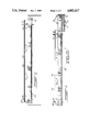
- FIG. 1 is a sectional end view through a wave soldering apparatus illustrating one embodiment of a solder receiving tray to restrict or limit formation of dross;
- FIG. 2 is a side view partially in section of the soldering apparatus shown in FIG. 1 illustrating a weir to control the level of solder in the solder receiving tray;
- FIG. 3 is a top plan view of the nozzle and solder receiving tray shown in FIG. 1;
- FIG. 4 is a side view partially in section showing a valve and float to control the level of solder in the solder receiving tray;
- FIG. 5 is a top plan view of the soldering apparatus shown in FIG. 4;
- FIG. 6 is an isometric view of an overflow solder dipping apparatus with a solder receiving tray according to the present invention.
- FIGS. 1, 2 and 3 show a solder reservoir 10 with a solder nozzle 12 through which molten liquid solder is pumped to a solder wave 14.
- Printed wiring boards 15 are conveyed in a conveyor path 16 so that pins and other areas to be soldered pass through the crest of the solder wave 14.
- An entry or upstream side of the solder wave is shown to have a contoured front plate 18 down which the solder flows in a non-turbulent fashion into the solder pot 10.
- a baffle 20 acts as a guide and is hinged to restrict solder flow at the bottom, thus can be set to provide a raised level above the dynamic solder level in the reservoir. The majority of solder flow from the wave flows to the entry side of the solder wave 14.
- solder from the solder wave flows in the trough and over the weir 24 at approximately the same speed as the conveyor 16 so that as the printed wiring board passes through and leaves the solder wave 14, there are no side icicles formed on pins and other soldered parts.
- solder receiving tray 26 Beneath the weir 24 is a solder receiving tray 26 which has an adjustable plate 28 at the downstream side to form a gate allowing some solder to flow from the tray 26 beneath the plate 28 to the reservoir 10. In most solder waves there is generally a drop of approximately two and a half to three inches from the crest of the solder wave to the dynamic solder level in the reservoir 10.
- the solder level in the tray 26 is kept at a predetermined distance below the weir 24 and in a preferred embodiment the distance from the lip of the weir 24 to the solder level in the tray 26 is in the range of an inch and a quarter to an inch and a half although this may be as much as an inch and three quarters.
- the adjustable plate 28 is adjustable by screws 30 to control the flow of solder through the gate into the solder reservoir 10.
- a level control weir 32 is positioned at at one end of the tray 26 so that it is away from the solder wave and also away from the conveyor 16 conveying articles through the solder wave 14.
- the level control weir 32 is a safety overflow device that controls the desired solder level in the tray 26. This level is selected so that optimum solder flow from the solder wave 14 over the weir 24 is achieved for soldering components conveyed along the conveyor path, and the formation of dross is limited as much as possible consistent with optimum solder flow.
- weir 24 on the exit side of the solder wave and the level control weir 32 at one end of the tray 26 so that the solder falls in two stages rather than a single stage. Furthermore, by permitting a portion of the solder flow to exit below the adjustable plate 28, less turbulence occurs and a reduction in dross is attained.
- dross can form in the liquid solder exiting through the gate below the adjustable plate 28. If this occurs, then more solder flows over the level control weir 32 at the end of the tray 26, but there is substantially no change in the solder level in the tray.
- the maximum level of the solder in the tray 26 is adjustable by varying the height of the level control weir 32.
- the bottom of the tray 26 is below the dynamic solder level in the reservoir, thus no free fall of solder occurs when solder flows through the gate.
- the bottom of the tray is illustrated as being flat, it may be sloped down to the gate to reduce the volume of solder retained in the tray.
- a tray may be provided which has a bottom that is above the dynamic solder level in the reservoir 10. In this case there is preferably a lower portion which has a gate with an exit below the dynamic solder level.
- FIGS. 4 and 5 illustrate another embodiment for controlling the level of solder in the solder receiving tray.
- a lower portion 40 extending down below the dynamic solder level in the reservoir 10.
- a valve 42 is positioned over a valve opening 44 in the lower portion 40.
- a valve stem 46 attached to the valve 42 extends up through a baffle plate 48 to a float 50.
- the float is attached to a threaded stem 46 so that by rotation of the float 50 relative to the stem 42 adjustment can be made to the solder level in the solder receiving tray 26.
- the baffle plate 48 extends over the area of the valve 42 and acts to prevent a vortex occurring in the solder when it exits through the valve opening 44.
- the buoyancy of the float 50 is selected to give a predetermined range of solder level in the tray 26 from valve opened to valve closed.
- the advantage of the valve system shown in FIGS. 4 and 5 is that no level control weir 32 is provided so no solder falls by free fall 32 into the reservoir 10. Instead of falling over a weir the solder flows through the valve opening 44 which is below the dynamic solder level in the reservoir thus minimum turbulence occurs.
- the solder level in the tray 26 remains substantially constant, preferably about 11/4 to 11/2 inches below the solder wave 14, regardless of how much solder flows through the gate under the adjustable plate 28.
- FIG. 4 shows the dynamic solder level below the bottom of the tray 26 so solder flowing under the plate 28 through the gate falls into the reservoir.
- at least a portion of the bottom of the tray with the gate therein is lowered below the dynamic solder level so the solder does not fall but flows through the gate.
- Tests conducted with the apparatus shown in FIGS. 3 and 4 allowed the skimming of dross of the surface of the reservoir 10 to be carried out at the end of an eight hour shift instead of every two hours or less which was common on similar devices not having the solder receiving tray 26.
- a solder dipping device is illustrated in FIG. 6 which has a rectangular dipping tank 60 for dipping such items as tin cans, radiators and other items requiring tinning or solder coating.
- a pump (not shown) pumps liquid metal, such as solder or tin, from a reservoir 62 below the dipping tank 60 so that the solder flows over the top edges of the tank 60 and falls in a free fall into a receiving tray 64 which surrounds the tank 60 forming a moat.
- a contoured flow plate for streamline flow may also be used.
- a lower portion 40 At one side of the tray is a lower portion 40 with a valve 42 similar to that shown in FIGS. 4 and 5.
- the level of the lower portion 40 is below the dynamic solder level in the reservoir 62 so no free fall of solder occurs from the tray 64 to the reservoir 62.
- an adjustable plate 28 is shown which may be raised up similar to that shown in FIG. 1 to provide a gate for solder to flow into the reservoir.
- the gate may not always be required if the valve opening 44 is sufficiently large to take all the solder flow over the top edges of the tank 60.
- FIGS. 1 to 5 show a specific design of solder wave device
- solder receiving tray of the present embodiment is shown extending along only the downstream portion of the solder wave. It would be apparent to those skilled in the art that this tray could also extend for the upstream portion as well as the downstream portion and in another embodiment may extend all around the solder wave in the form of a moat so that there was an intermediate solder receiving tray to catch all of the solder from the solder wave to prevent there being a large fall of solder, thus minimizing the dross formation.
Landscapes
- Engineering & Computer Science (AREA)
- Mechanical Engineering (AREA)
- Molten Solder (AREA)
- Electric Connection Of Electric Components To Printed Circuits (AREA)
Abstract
Description
Claims (19)
Priority Applications (1)
| Application Number | Priority Date | Filing Date | Title |
|---|---|---|---|
| US07/158,308 US4802617A (en) | 1988-02-19 | 1988-02-19 | Restriction of dross formation in a soldering apparatus |
Applications Claiming Priority (1)
| Application Number | Priority Date | Filing Date | Title |
|---|---|---|---|
| US07/158,308 US4802617A (en) | 1988-02-19 | 1988-02-19 | Restriction of dross formation in a soldering apparatus |
Publications (1)
| Publication Number | Publication Date |
|---|---|
| US4802617A true US4802617A (en) | 1989-02-07 |
Family
ID=22567524
Family Applications (1)
| Application Number | Title | Priority Date | Filing Date |
|---|---|---|---|
| US07/158,308 Expired - Fee Related US4802617A (en) | 1988-02-19 | 1988-02-19 | Restriction of dross formation in a soldering apparatus |
Country Status (1)
| Country | Link |
|---|---|
| US (1) | US4802617A (en) |
Cited By (16)
| Publication number | Priority date | Publication date | Assignee | Title |
|---|---|---|---|---|
| WO1991015327A1 (en) * | 1990-04-06 | 1991-10-17 | Electrovert Ltd. | Weir and gate adjustment device for solder wave nozzle |
| US5379931A (en) * | 1992-01-14 | 1995-01-10 | Soltec B.V. | Soldering apparatus with improved configuration of solder streams |
| US6126060A (en) * | 1998-07-03 | 2000-10-03 | Samsung Electronics Co., Ltd. | Soldering device |
| US6364195B1 (en) * | 1996-06-11 | 2002-04-02 | Kabushiki Kaisha Tamura Seisakusho | Brazing Apparatus |
| US6431431B2 (en) | 2000-03-09 | 2002-08-13 | Speedline Technologies, Inc. | Apparatus and methods for wave soldering |
| US6499650B2 (en) * | 2000-09-07 | 2002-12-31 | Senju Metal Industry Co., Ltd. | Solder dross removal apparatus and method |
| US6592017B2 (en) | 2001-01-12 | 2003-07-15 | Speedline Technologies, Inc. | Automatic dross removal apparatus and method |
| US6666370B2 (en) | 2002-01-18 | 2003-12-23 | Speedline Technologies, Inc. | Solder-dross mixture separation method and apparatus |
| US6948650B2 (en) | 2001-01-12 | 2005-09-27 | Speedline Technologies, Inc. | Dross removal and solder reclamation improvements |
| EP1859886A1 (en) * | 2005-03-18 | 2007-11-28 | Senju Metal Industry Co., Ltd. | Jet solder vessel |
| WO2007138310A2 (en) * | 2006-05-30 | 2007-12-06 | Pillarhouse International Limited | Soldering apparatus |
| US20110226843A1 (en) * | 2010-03-16 | 2011-09-22 | Flextronics Ap, Llc | Solder return for wave solder nozzle |
| US20110293903A1 (en) * | 2010-05-25 | 2011-12-01 | Samsung Electronics Co., Ltd. | Wave soldering apparatus to apply buoyancy, soldering method, and method of forming solder bumps for flip chips on a substrate |
| WO2013020290A1 (en) * | 2011-08-11 | 2013-02-14 | Linde Aktiengesellschaft | Device and method for wave soldering of workpieces with solder recirculation |
| CN104294199A (en) * | 2014-10-20 | 2015-01-21 | 天津普林电路股份有限公司 | Solder recovery device for hot wind tin spraying process of high density interconnected circuit board |
| US9370838B2 (en) | 2014-08-21 | 2016-06-21 | Illinois Tool Works Inc. | Wave soldering nozzle system and method of wave soldering |
Citations (5)
| Publication number | Priority date | Publication date | Assignee | Title |
|---|---|---|---|---|
| US3921888A (en) * | 1974-10-07 | 1975-11-25 | Electrovert Inc | Wave soldering of printed circuits |
| US4171761A (en) * | 1978-03-20 | 1979-10-23 | Rockwell International Corporation | Wave solder apparatus |
| US4666077A (en) * | 1983-02-28 | 1987-05-19 | Electrovert | Solder pot for wave soldering machine |
| US4679720A (en) * | 1986-10-23 | 1987-07-14 | Hollis Automation, Inc. | Mass soldering system providing a sweeping fluid blast |
| US4684056A (en) * | 1985-05-03 | 1987-08-04 | Electrovert Limited | Vibratory wave soldering |
-
1988
- 1988-02-19 US US07/158,308 patent/US4802617A/en not_active Expired - Fee Related
Patent Citations (6)
| Publication number | Priority date | Publication date | Assignee | Title |
|---|---|---|---|---|
| US3921888A (en) * | 1974-10-07 | 1975-11-25 | Electrovert Inc | Wave soldering of printed circuits |
| US3921888B1 (en) * | 1974-10-07 | 1993-01-12 | Electrovert Ltd | |
| US4171761A (en) * | 1978-03-20 | 1979-10-23 | Rockwell International Corporation | Wave solder apparatus |
| US4666077A (en) * | 1983-02-28 | 1987-05-19 | Electrovert | Solder pot for wave soldering machine |
| US4684056A (en) * | 1985-05-03 | 1987-08-04 | Electrovert Limited | Vibratory wave soldering |
| US4679720A (en) * | 1986-10-23 | 1987-07-14 | Hollis Automation, Inc. | Mass soldering system providing a sweeping fluid blast |
Cited By (26)
| Publication number | Priority date | Publication date | Assignee | Title |
|---|---|---|---|---|
| WO1991015327A1 (en) * | 1990-04-06 | 1991-10-17 | Electrovert Ltd. | Weir and gate adjustment device for solder wave nozzle |
| US5379931A (en) * | 1992-01-14 | 1995-01-10 | Soltec B.V. | Soldering apparatus with improved configuration of solder streams |
| US6364195B1 (en) * | 1996-06-11 | 2002-04-02 | Kabushiki Kaisha Tamura Seisakusho | Brazing Apparatus |
| US6126060A (en) * | 1998-07-03 | 2000-10-03 | Samsung Electronics Co., Ltd. | Soldering device |
| US6431431B2 (en) | 2000-03-09 | 2002-08-13 | Speedline Technologies, Inc. | Apparatus and methods for wave soldering |
| US6499650B2 (en) * | 2000-09-07 | 2002-12-31 | Senju Metal Industry Co., Ltd. | Solder dross removal apparatus and method |
| US6592017B2 (en) | 2001-01-12 | 2003-07-15 | Speedline Technologies, Inc. | Automatic dross removal apparatus and method |
| US6948650B2 (en) | 2001-01-12 | 2005-09-27 | Speedline Technologies, Inc. | Dross removal and solder reclamation improvements |
| US6666370B2 (en) | 2002-01-18 | 2003-12-23 | Speedline Technologies, Inc. | Solder-dross mixture separation method and apparatus |
| US20090050674A1 (en) * | 2005-03-18 | 2009-02-26 | Mitsuo Zen | Wave Soldering Bath |
| EP1859886A1 (en) * | 2005-03-18 | 2007-11-28 | Senju Metal Industry Co., Ltd. | Jet solder vessel |
| US7988030B2 (en) * | 2005-03-18 | 2011-08-02 | Senju Metal Industry Co., Ltd. | Wave soldering bath |
| EP1859886B1 (en) * | 2005-03-18 | 2016-10-12 | Senju Metal Industry Co., Ltd. | Jet solder vessel |
| CN101454109B (en) * | 2006-05-30 | 2012-03-21 | 皮乐豪斯国际有限公司 | Soldering apparatus |
| WO2007138310A3 (en) * | 2006-05-30 | 2008-04-10 | Pillarhouse Int Ltd | Soldering apparatus |
| WO2007138310A2 (en) * | 2006-05-30 | 2007-12-06 | Pillarhouse International Limited | Soldering apparatus |
| CN102883846A (en) * | 2010-03-16 | 2013-01-16 | 弗莱克斯电子有限责任公司 | Solder return for wave solder nozzle |
| US8146792B2 (en) * | 2010-03-16 | 2012-04-03 | Flextronics Ap, Llc | Solder return for wave solder nozzle |
| US8424743B2 (en) | 2010-03-16 | 2013-04-23 | Flextronics Ap, Llc | Solder return for wave solder nozzle |
| US8453915B2 (en) | 2010-03-16 | 2013-06-04 | Flextronics Ap, Llc | Solder return for wave solder nozzle |
| CN102883846B (en) * | 2010-03-16 | 2015-12-16 | 弗莱克斯电子有限责任公司 | Solder for wave soldering nozzle reclaims |
| US20110226843A1 (en) * | 2010-03-16 | 2011-09-22 | Flextronics Ap, Llc | Solder return for wave solder nozzle |
| US20110293903A1 (en) * | 2010-05-25 | 2011-12-01 | Samsung Electronics Co., Ltd. | Wave soldering apparatus to apply buoyancy, soldering method, and method of forming solder bumps for flip chips on a substrate |
| WO2013020290A1 (en) * | 2011-08-11 | 2013-02-14 | Linde Aktiengesellschaft | Device and method for wave soldering of workpieces with solder recirculation |
| US9370838B2 (en) | 2014-08-21 | 2016-06-21 | Illinois Tool Works Inc. | Wave soldering nozzle system and method of wave soldering |
| CN104294199A (en) * | 2014-10-20 | 2015-01-21 | 天津普林电路股份有限公司 | Solder recovery device for hot wind tin spraying process of high density interconnected circuit board |
Similar Documents
| Publication | Publication Date | Title |
|---|---|---|
| US4802617A (en) | Restriction of dross formation in a soldering apparatus | |
| EP0083680B1 (en) | Wavesoldering of chips | |
| US4171761A (en) | Wave solder apparatus | |
| US3921888A (en) | Wave soldering of printed circuits | |
| EP0688254B1 (en) | Solder nozzle with gas knife jet | |
| US8424743B2 (en) | Solder return for wave solder nozzle | |
| EP0015734A1 (en) | Paint spray booth with water curtain | |
| US4886201A (en) | Solder wave nozzle construction | |
| US3990621A (en) | Static head soldering system with oil | |
| KR910000478A (en) | Distributor of fluid feed | |
| US5379931A (en) | Soldering apparatus with improved configuration of solder streams | |
| US5244573A (en) | Paint sludge separator tank | |
| US4599966A (en) | Solder leveller | |
| US5630542A (en) | Soldering apparatus with abrupt separation of solder streams | |
| CA1195880A (en) | Wave soldering apparatus and method | |
| US4635584A (en) | Apparatus for tinning printed-circuit boards | |
| JPS6222295Y2 (en) | ||
| US5422003A (en) | Gas-liquid separation flow rate regulator in sewage disposal tank | |
| RU2100137C1 (en) | Gear to feed melt in plant for continuous casting of aluminium | |
| JP2820260B2 (en) | Jet type soldering equipment | |
| JPH0280169A (en) | Automatic jet type soldering device | |
| JPH0573510B2 (en) | ||
| CA1310547C (en) | Soldering device | |
| CA2155351C (en) | Solder nozzle with gas knife jet | |
| JPH0677815B2 (en) | Jet type solder bath |
Legal Events
| Date | Code | Title | Description |
|---|---|---|---|
| AS | Assignment |
Owner name: ELECTROVERT LIMITED, 44 DUFFLAW ROAD, TORONTO, ONT Free format text: ASSIGNMENT OF ASSIGNORS INTEREST.;ASSIGNOR:DEAMBROSIO, CARLOS A.;REEL/FRAME:004875/0042 Effective date: 19880217 Owner name: ELECTROVERT LIMITED,CANADA Free format text: ASSIGNMENT OF ASSIGNORS INTEREST;ASSIGNOR:DEAMBROSIO, CARLOS A.;REEL/FRAME:004875/0042 Effective date: 19880217 |
|
| FPAY | Fee payment |
Year of fee payment: 4 |
|
| REMI | Maintenance fee reminder mailed | ||
| LAPS | Lapse for failure to pay maintenance fees | ||
| FP | Lapsed due to failure to pay maintenance fee |
Effective date: 19970212 |
|
| AS | Assignment |
Owner name: SPEEDLINE TECHNOLOGIES, INC., MASSACHUSETTS Free format text: ASSIGNMENT OF ASSIGNORS INTEREST;ASSIGNOR:COOKSON CANADA, INC.;REEL/FRAME:016026/0230 Effective date: 20050317 |
|
| AS | Assignment |
Owner name: COOKSON CANADA, INC., CANADA Free format text: MERGER;ASSIGNOR:ELECTROVERT LTD.;REEL/FRAME:017649/0001 Effective date: 20031217 |
|
| STCH | Information on status: patent discontinuation |
Free format text: PATENT EXPIRED DUE TO NONPAYMENT OF MAINTENANCE FEES UNDER 37 CFR 1.362 |