US4790642A - Integrated metrology for microlithographic objective reducing lens - Google Patents
Integrated metrology for microlithographic objective reducing lens Download PDFInfo
- Publication number
- US4790642A US4790642A US06/936,245 US93624586A US4790642A US 4790642 A US4790642 A US 4790642A US 93624586 A US93624586 A US 93624586A US 4790642 A US4790642 A US 4790642A
- Authority
- US
- United States
- Prior art keywords
- block
- metrology
- lens
- pair
- central opening
- Prior art date
- Legal status (The legal status is an assumption and is not a legal conclusion. Google has not performed a legal analysis and makes no representation as to the accuracy of the status listed.)
- Expired - Fee Related
Links
Images


Classifications
-
- G—PHYSICS
- G03—PHOTOGRAPHY; CINEMATOGRAPHY; ANALOGOUS TECHNIQUES USING WAVES OTHER THAN OPTICAL WAVES; ELECTROGRAPHY; HOLOGRAPHY
- G03F—PHOTOMECHANICAL PRODUCTION OF TEXTURED OR PATTERNED SURFACES, e.g. FOR PRINTING, FOR PROCESSING OF SEMICONDUCTOR DEVICES; MATERIALS THEREFOR; ORIGINALS THEREFOR; APPARATUS SPECIALLY ADAPTED THEREFOR
- G03F7/00—Photomechanical, e.g. photolithographic, production of textured or patterned surfaces, e.g. printing surfaces; Materials therefor, e.g. comprising photoresists; Apparatus specially adapted therefor
- G03F7/70—Microphotolithographic exposure; Apparatus therefor
- G03F7/708—Construction of apparatus, e.g. environment aspects, hygiene aspects or materials
- G03F7/70808—Construction details, e.g. housing, load-lock, seals or windows for passing light in or out of apparatus
- G03F7/70825—Mounting of individual elements, e.g. mounts, holders or supports
-
- G—PHYSICS
- G01—MEASURING; TESTING
- G01B—MEASURING LENGTH, THICKNESS OR SIMILAR LINEAR DIMENSIONS; MEASURING ANGLES; MEASURING AREAS; MEASURING IRREGULARITIES OF SURFACES OR CONTOURS
- G01B9/00—Measuring instruments characterised by the use of optical techniques
- G01B9/04—Measuring microscopes
-
- G—PHYSICS
- G02—OPTICS
- G02B—OPTICAL ELEMENTS, SYSTEMS OR APPARATUS
- G02B13/00—Optical objectives specially designed for the purposes specified below
- G02B13/24—Optical objectives specially designed for the purposes specified below for reproducing or copying at short object distances
-
- G—PHYSICS
- G03—PHOTOGRAPHY; CINEMATOGRAPHY; ANALOGOUS TECHNIQUES USING WAVES OTHER THAN OPTICAL WAVES; ELECTROGRAPHY; HOLOGRAPHY
- G03F—PHOTOMECHANICAL PRODUCTION OF TEXTURED OR PATTERNED SURFACES, e.g. FOR PRINTING, FOR PROCESSING OF SEMICONDUCTOR DEVICES; MATERIALS THEREFOR; ORIGINALS THEREFOR; APPARATUS SPECIALLY ADAPTED THEREFOR
- G03F9/00—Registration or positioning of originals, masks, frames, photographic sheets or textured or patterned surfaces, e.g. automatically
- G03F9/70—Registration or positioning of originals, masks, frames, photographic sheets or textured or patterned surfaces, e.g. automatically for microlithography
Definitions
- Microlithographic objective reducing lenses are used for reducing and imaging patterns for electronic microcircuits on semi-conductor wafers.
- the microlithography industry seeks ever-greater accuracy in the registration and imaging to facilitate miniaturizing the circuitry and to preserve accuracy and reliability in the final product.
- any substantial increase in accuracy for microlithographic objective reducing lenses is a welcome advance in this art.
- Metrology for microlithographic objective reducing lenses is necessary for referencing the wafer relative to the lens to ensure that the desired interrelationship between the lens and the wafer is maintained as accurately as possible.
- Six degrees of freedom of relative motion are possible and include X and Y registration in the plane of the wafer surface, Z axis distance between the lens and the wafer, tip and tilt angles between the lens and wafer, and the rotational angle of the wafer around the Z axis of the lens.
- Computers are programmed to control the movements involved, and detectors or sensors for gathering information on the position of the wafer relative to the lens are included within the metrology components.
- Our metrology for a microlithographic objective reducing lens is integrated into a block secured to a lower region of the barrel for the lens.
- the block has a central opening around a lowermost element of the lens, and the block is otherwise securely mounted on the lens barrel to ensure an accurate relation between the block and the lowermost lens element.
- the metrology components integrated into the block include distance detectors arranged on the block to face downward around the central opening, a pair of microscope objectives mounted on the block outside the central opening, and a pair of X and Y mirrors also mounted on the block. All these components are then spaced only a short distance from the lowermost lens element in positions that are stabilized by the block to improve the accuracy of the metrology system based on these components.
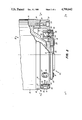
- FIG. 1 is a partially cross-sectioned, and partially schematic elevational view of a lower region of a microlithographic objective reducing lens having metrology components integrated with the lens barrel according to our invention
- FIG. 2 is an enlarged and partially sectioned, side elevational view of the metrology block at the lower end of the lens shown in FIG. 1;
- FIG. 3 is a bottom view of the metrology block of FIG. 2;
- FIG. 4 is a plan view of the metrology block of FIG. 2, separated from the lower region of the lens barrel.
- Microlithographic objective reducing lens 10 is shown partially cut away and emptied of all but the lowermost element 11 of its many lens elements, which are carefully assembled with the highest possible accuracy into generally cylindrical lens barrel 15. Some parts have been eliminated for simplicity, and the controlled environment in which lens 10 operates is also not illustrated.
- the metrology used to control the positional interrelationships, between wafer 13 and lens 10 enjoys better accuracy, we find, when it is closely and accurately associated with lowermost surface 12 of lens element 11.
- metrology block 20 to contain and mount metrology components and to fasten directly and securely to a lower region of lens barrel 15.
- the metrology components that we prefer include a capacitive distance detector 25 having four elements 28, a pair of microscope objectives 30 and 31, and X and Y reference mirrors 40 and 41.
- capacitive distance detector 25 for metrology block 20
- alternative distance detectors such as pneumatic gauging or optical transducers could also be used for measurements in the Z axis direction.
- metrology components on block 20 be mounted within the outside diameter of lens barrel 15.
- metrology block 20 in two main parts that include a generally circular ring 21 fastened to a lower region of lens barrel 15 and an annular sensor plate 22 fastened to ring 21.
- Three screws 23 secure ring 21 to lens barrel 15, and ring 21 has small locator feet 24 surrounding each of the screws 23 for accurately locating the plane of ring 21 relative to lens barrel 15.
- Three screws 26 fasten sensor plate 22 to ring 21 and locate the plane of plate 22 relative to ring 21 in a similar way.
- Ring 21 and plate 22 can also be machined as a single unit.
- metrology block 20 be formed of a dimensionally stable material, such as a ceramic or an Invar alloy of nickel and iron.
- the material of block 20 should be dimensionally stable within one millionth of an inch during an indefinite lifetime in a controlled environment. Dimensional stability to maintain the positional relationships of the metrology components to lowermost lens element 11 is more important than any specific shape or dimensions.
- Plate 22 has a central opening 27 around lowermost element surface 12, and capacitive distance detector 25, with its elements 28, is preferably arranged on a downward facing surface of plate 22 around central opening 27 and within guard ring 19. This disposes distance detector 25 in as close a relationship as possible with lowermost element surface 12 for measuring the distance to the upper surface of wafer 13. Since room is available, some of the electronics 29 for capacitive distance detector 25 are mounted on sensor plate 22 as schematically shown.
- Microscope objectives 30 and 31 are threaded into mounts 32 that are arranged in holes in sensor plate 22. Each mount 32 is held in place by collars 33 on screws 34 so that objectives 30 and 31, and their beam-reflecting prisms 35, are rotatable relative to plate 22 for alignment purposes. Objectives 31 and 32 are also vertically adjustable relative to plate 22 by means of shims or spacers 38. Bore holes 36 and 37 through ring 21 afford passageways through which beams from the microscope objectives are transmitted outward. We direct these beams to video cameras, either through a conventional optical transmission path outside of lens barrel 15 or via fiber optic cables. Microscope objectives 30 and 31 are preferably arranged within the inside diameter of lens barrel 15 and outside of central opening 27.
- microscope objectives can also be arranged elsewhere. In our positioning of objectives 30 and 31, they are spaced only an inch and a half from the lens axis and only three inches apart. This improves on the stability attainable with microscope objectives positioned outside of lens barrel 15 at a greater distance from the lens axis.
- Each mirror 40 and 41 mounts on a three-point stand 45, two points of which are adjustment screws 46 surrounded by spring washers 47 and threaded into ring 21.
- the other point for each stand 45 is a ball bearing 48 held between ring 21 and stand 45 by a spring clip 49.
- Reference mirrors 40 and 41 can be accurately aligned relative to the beams of fringe-counting interferometers by adjusting screws 46.
- the preferred metrology components as arranged in metrology block 20, provide information for all six degrees of freedom of relative motion between lens 10 and wafer 13.
- Microscope objectives 30 and 31 can be registered with location marks made on an upper surface of wafer 13, and we prefer registering one microscope objective with its respective location mark and then rotating the wafer relative to the lens to register the other mark with the other microscope objective. This establishes an X, Y reference that is also correct for rotational angle.
- the microscope objectives preferably have a field of view larger than the location marks to facilitate this registration, which is preferably made visible on a video monitor.
- the wafer is movable under the lens in the X and Y directions under control of fringe-counting interferometers that use mirrors 40 and 41 as reference mirrors and use similar mirrors (not shown) on the wafer-moving stage as test mirrors.
- fringe-counting interferometers that use mirrors 40 and 41 as reference mirrors and use similar mirrors (not shown) on the wafer-moving stage as test mirrors.
- Capacitive distance detector 25 is highly accurate in measuring the distance to the upper surface of wafer 13. Since distance detector 25 has at least three and preferably four elements 28, these can detect tip and tilt angles between lens 10 and the top surface of wafer 13. It is even possible for our metrology to scan and map the topography of the top surface of wafer 13 before imaging the wafer so as to make adjustments based on knowledge of the topography during the imaging process. We prefer that the plane of distance detector 25 be within about one-half a millimeter of wafer 13 for a working range at which a capacitive distance detector is highly accurate. Other distances may apply for distance detectors operating pneumatically or with optical transducers.
- the close association of distance detector 25 with lowermost element surface 12 assures that distance and tip and tilt angle measurements are made more accurately than with existing methods.
- the positioning of microscope objectives 30 and 31 close to element 11, and preferably within the inside diameter of lens barrel 15, improves their stability and long-term accuracy relative to prior art locations spaced outside of lens barrel 15.
- Locating reference mirrors 40 and 41 directly on the machined rim of metrology block 20, and preferably within the outside diameter of lens barrel 15, also assures a simple, direct, and highly accurate relationship between these mirrors and lens element 11.
- the dimensionally stable support that metrology block 20 gives to all these components helps maintain the accuracy they can attain.
- our metrology arrangement substantially improves the accuracy of the positioning of our microlithographic objective reducing lens relative to the wafer, compared to the previously attainable accuracy.
- Our accuracy improvement is by an order of magnitude; and at the same time, our metrology arrangement is simpler and less expensive than prior art metrology systems arranged outside of lens barrel 15.
Abstract
Description
Claims (36)
Priority Applications (3)
| Application Number | Priority Date | Filing Date | Title |
|---|---|---|---|
| US06/936,245 US4790642A (en) | 1986-12-01 | 1986-12-01 | Integrated metrology for microlithographic objective reducing lens |
| DE19873740537 DE3740537A1 (en) | 1986-12-01 | 1987-11-30 | INTEGRATED MEASURING ARRANGEMENT FOR MICROLITHOGRAPHIC REDUCTION LENSES |
| JP62304389A JPS63155616A (en) | 1986-12-01 | 1987-12-01 | Unified measurement apparatus of contraction object lens for circuit printing |
Applications Claiming Priority (1)
| Application Number | Priority Date | Filing Date | Title |
|---|---|---|---|
| US06/936,245 US4790642A (en) | 1986-12-01 | 1986-12-01 | Integrated metrology for microlithographic objective reducing lens |
Publications (1)
| Publication Number | Publication Date |
|---|---|
| US4790642A true US4790642A (en) | 1988-12-13 |
Family
ID=25468369
Family Applications (1)
| Application Number | Title | Priority Date | Filing Date |
|---|---|---|---|
| US06/936,245 Expired - Fee Related US4790642A (en) | 1986-12-01 | 1986-12-01 | Integrated metrology for microlithographic objective reducing lens |
Country Status (3)
| Country | Link |
|---|---|
| US (1) | US4790642A (en) |
| JP (1) | JPS63155616A (en) |
| DE (1) | DE3740537A1 (en) |
Cited By (7)
| Publication number | Priority date | Publication date | Assignee | Title |
|---|---|---|---|---|
| US5945790A (en) * | 1997-11-17 | 1999-08-31 | Schaefer; Raymond B. | Surface discharge lamp |
| US20050168843A1 (en) * | 2003-12-24 | 2005-08-04 | Carl Zeiss Jena Gmbh | Microscope objective with axially adjustable correction mounts |
| WO2006128713A2 (en) * | 2005-06-02 | 2006-12-07 | Carl Zeiss Smt Ag | Optical imaging arrangement |
| US20080291413A1 (en) * | 2007-05-24 | 2008-11-27 | Asml Netherlands B.V. | Lithographic apparatus having encoder type position sensor system |
| US20090002653A1 (en) * | 2007-05-24 | 2009-01-01 | Asml Netherlands B.V. | Lithographic apparatus having encoder type position sensor system |
| CN102637340A (en) * | 2012-03-14 | 2012-08-15 | 上海华力微电子有限公司 | Method for preventing microscope on Cascade probe station from striking probe |
| DE102011077223A1 (en) * | 2011-06-08 | 2012-12-13 | Carl Zeiss Smt Gmbh | measuring system |
Citations (18)
| Publication number | Priority date | Publication date | Assignee | Title |
|---|---|---|---|---|
| US3577791A (en) * | 1969-01-22 | 1971-05-04 | Conduction Corp | Control system |
| US3825323A (en) * | 1973-05-17 | 1974-07-23 | Teletype Corp | Rotary disc recording and readout system having capacitance controlled lens positioning means |
| US3953133A (en) * | 1973-07-11 | 1976-04-27 | Ernst Leitz G.M.B.H. | Method of determining the angular position of a workpiece and apparatus therefor |
| US4027976A (en) * | 1974-05-13 | 1977-06-07 | Jenoptik Jena G.M.B.H. | Optical interferometer |
| US4139304A (en) * | 1977-02-10 | 1979-02-13 | National Research Development Corporation | Methods and apparatus for measuring variations in distance to a surface |
| US4311390A (en) * | 1979-02-27 | 1982-01-19 | Optimetrix Corporation | Interferometrically controlled stage with precisely orthogonal axes of motion |
| US4328553A (en) * | 1976-12-07 | 1982-05-04 | Computervision Corporation | Method and apparatus for targetless wafer alignment |
| US4362385A (en) * | 1979-02-14 | 1982-12-07 | Censor Patent-Und Versuchsanstalt | Process and arrangement for copying masks on a workpiece with arrangement for correction of alignment errors |
| US4385838A (en) * | 1980-01-19 | 1983-05-31 | Nippon Kogaku K. K. | Alignment device |
| US4398824A (en) * | 1981-04-15 | 1983-08-16 | Bell Telephone Laboratories, Incorporated | Wafer tilt compensation in zone plate alignment system |
| US4539835A (en) * | 1983-10-28 | 1985-09-10 | Control Data Corporation | Calibration apparatus for capacitance height gauges |
| US4573791A (en) * | 1979-04-03 | 1986-03-04 | Optimetrix Corporation | Step-and-repeat projection alignment and exposure system |
| US4580900A (en) * | 1982-04-02 | 1986-04-08 | Eaton Corporation | Auto focus alignment and measurement system and method |
| EP0189869A2 (en) * | 1985-01-28 | 1986-08-06 | Edward H. Phillips | Improved step-and-repeat aligment and exposure system and method therefore |
| US4615621A (en) * | 1982-04-02 | 1986-10-07 | Eaton Corporation | Auto-focus alignment and measurement system and method |
| US4638486A (en) * | 1984-06-25 | 1987-01-20 | Siemens Aktiengesellschaft | Adjustment device for a reflector mirror of a laser resonator |
| US4654581A (en) * | 1983-10-12 | 1987-03-31 | Hewlett-Packard Company | Capacitive mask aligner |
| US4686531A (en) * | 1983-10-28 | 1987-08-11 | Control Data Corporation | Capacitance height gage applied in reticle position detection system for electron beam lithography apparatus |
-
1986
- 1986-12-01 US US06/936,245 patent/US4790642A/en not_active Expired - Fee Related
-
1987
- 1987-11-30 DE DE19873740537 patent/DE3740537A1/en not_active Withdrawn
- 1987-12-01 JP JP62304389A patent/JPS63155616A/en active Pending
Patent Citations (18)
| Publication number | Priority date | Publication date | Assignee | Title |
|---|---|---|---|---|
| US3577791A (en) * | 1969-01-22 | 1971-05-04 | Conduction Corp | Control system |
| US3825323A (en) * | 1973-05-17 | 1974-07-23 | Teletype Corp | Rotary disc recording and readout system having capacitance controlled lens positioning means |
| US3953133A (en) * | 1973-07-11 | 1976-04-27 | Ernst Leitz G.M.B.H. | Method of determining the angular position of a workpiece and apparatus therefor |
| US4027976A (en) * | 1974-05-13 | 1977-06-07 | Jenoptik Jena G.M.B.H. | Optical interferometer |
| US4328553A (en) * | 1976-12-07 | 1982-05-04 | Computervision Corporation | Method and apparatus for targetless wafer alignment |
| US4139304A (en) * | 1977-02-10 | 1979-02-13 | National Research Development Corporation | Methods and apparatus for measuring variations in distance to a surface |
| US4362385A (en) * | 1979-02-14 | 1982-12-07 | Censor Patent-Und Versuchsanstalt | Process and arrangement for copying masks on a workpiece with arrangement for correction of alignment errors |
| US4311390A (en) * | 1979-02-27 | 1982-01-19 | Optimetrix Corporation | Interferometrically controlled stage with precisely orthogonal axes of motion |
| US4573791A (en) * | 1979-04-03 | 1986-03-04 | Optimetrix Corporation | Step-and-repeat projection alignment and exposure system |
| US4385838A (en) * | 1980-01-19 | 1983-05-31 | Nippon Kogaku K. K. | Alignment device |
| US4398824A (en) * | 1981-04-15 | 1983-08-16 | Bell Telephone Laboratories, Incorporated | Wafer tilt compensation in zone plate alignment system |
| US4580900A (en) * | 1982-04-02 | 1986-04-08 | Eaton Corporation | Auto focus alignment and measurement system and method |
| US4615621A (en) * | 1982-04-02 | 1986-10-07 | Eaton Corporation | Auto-focus alignment and measurement system and method |
| US4654581A (en) * | 1983-10-12 | 1987-03-31 | Hewlett-Packard Company | Capacitive mask aligner |
| US4539835A (en) * | 1983-10-28 | 1985-09-10 | Control Data Corporation | Calibration apparatus for capacitance height gauges |
| US4686531A (en) * | 1983-10-28 | 1987-08-11 | Control Data Corporation | Capacitance height gage applied in reticle position detection system for electron beam lithography apparatus |
| US4638486A (en) * | 1984-06-25 | 1987-01-20 | Siemens Aktiengesellschaft | Adjustment device for a reflector mirror of a laser resonator |
| EP0189869A2 (en) * | 1985-01-28 | 1986-08-06 | Edward H. Phillips | Improved step-and-repeat aligment and exposure system and method therefore |
Cited By (19)
| Publication number | Priority date | Publication date | Assignee | Title |
|---|---|---|---|---|
| US5945790A (en) * | 1997-11-17 | 1999-08-31 | Schaefer; Raymond B. | Surface discharge lamp |
| US7271966B2 (en) * | 2003-12-24 | 2007-09-18 | Carl Zeiss Jena Gmbh | Microscope objective with axially adjustable correction mounts |
| US20050168843A1 (en) * | 2003-12-24 | 2005-08-04 | Carl Zeiss Jena Gmbh | Microscope objective with axially adjustable correction mounts |
| US7817248B2 (en) | 2005-06-02 | 2010-10-19 | Carl Zeiss Smt Ag | Optical imaging arrangement |
| US20080212083A1 (en) * | 2005-06-02 | 2008-09-04 | Carl Zeiss Smt Ag | Optical imaging arrangement |
| WO2006128713A2 (en) * | 2005-06-02 | 2006-12-07 | Carl Zeiss Smt Ag | Optical imaging arrangement |
| US20110001949A1 (en) * | 2005-06-02 | 2011-01-06 | Carl Zeiss Smt Ag | Optical imaging arrangement |
| CN102929104B (en) * | 2005-06-02 | 2016-08-03 | 卡尔蔡司Smt有限责任公司 | Optical imaging device |
| US8416392B2 (en) | 2005-06-02 | 2013-04-09 | Carl Zeiss Smt Gmbh | Optical imaging arrangement |
| WO2006128713A3 (en) * | 2005-06-02 | 2007-05-31 | Zeiss Carl Smt Ag | Optical imaging arrangement |
| US8760615B2 (en) * | 2007-05-24 | 2014-06-24 | Asml Netherlands B.V. | Lithographic apparatus having encoder type position sensor system |
| US20080291413A1 (en) * | 2007-05-24 | 2008-11-27 | Asml Netherlands B.V. | Lithographic apparatus having encoder type position sensor system |
| US20090002653A1 (en) * | 2007-05-24 | 2009-01-01 | Asml Netherlands B.V. | Lithographic apparatus having encoder type position sensor system |
| US8836913B2 (en) | 2007-05-24 | 2014-09-16 | Asml Netherlands B.V. | Lithographic apparatus having an encoder type position sensor system |
| US8687166B2 (en) * | 2007-05-24 | 2014-04-01 | Asml Netherlands B.V. | Lithographic apparatus having an encoder position sensor system |
| DE102011077223B4 (en) * | 2011-06-08 | 2013-08-14 | Carl Zeiss Smt Gmbh | measuring system |
| DE102011077223A1 (en) * | 2011-06-08 | 2012-12-13 | Carl Zeiss Smt Gmbh | measuring system |
| US9482968B2 (en) | 2011-06-08 | 2016-11-01 | Carl Zeiss Smt Gmbh | Measuring system |
| CN102637340A (en) * | 2012-03-14 | 2012-08-15 | 上海华力微电子有限公司 | Method for preventing microscope on Cascade probe station from striking probe |
Also Published As
| Publication number | Publication date |
|---|---|
| DE3740537A1 (en) | 1988-06-16 |
| JPS63155616A (en) | 1988-06-28 |
Similar Documents
| Publication | Publication Date | Title |
|---|---|---|
| US7359047B2 (en) | Device for checking or calibrating the angle-dependent alignment of a high-precision test piece | |
| EP1014138B1 (en) | Apparatus and method for precision adjustment of the angular position of an optical device | |
| US6072569A (en) | Apparatus and a method for measurement of wedge in optical components | |
| EP0342639B2 (en) | Microlithographic apparatus | |
| US6172373B1 (en) | Stage apparatus with improved positioning capability | |
| US20020148133A1 (en) | Scale-bar artifact and methods of use | |
| US4717251A (en) | Elevation measurement in high order surveying | |
| WO2008067561A2 (en) | Interior contour measurement probe | |
| CN100360894C (en) | Laser interferometer for repeatable mounting on the wall of a vacuum chamber | |
| US6188078B1 (en) | Optical metrology device for precision angular measurement of a pointing mirror | |
| US4790642A (en) | Integrated metrology for microlithographic objective reducing lens | |
| US5532815A (en) | System and method for aligning a first surface with respect to a second surface | |
| US11754934B2 (en) | Projection exposure apparatus for semiconductor lithography having an optical element with sensor reference and method for aligning the sensor reference | |
| US5847820A (en) | Laser apparatus for sensing rotational orientation and levelness | |
| US4812654A (en) | Two-axis quartz fiber passive tilt meter | |
| US4270048A (en) | Apparatus for determining the angle of incident electromagnetic radiation | |
| US20080100930A1 (en) | Optical measuring system, and a projection objective | |
| US5123736A (en) | Method for determining the misalignment in the horizontal plane of elongated parts of a machine, such as cylinders and rollers, and an optical reflection instrument suitable for use with this method | |
| JPH04268433A (en) | Measuring apparatus for aspherical lens eccentricity | |
| JP4072265B2 (en) | Rotation axis tilt measurement method | |
| Washer et al. | Calibration of precision airplane mapping cameras | |
| JPH07229812A (en) | Eccentricity measuring apparatus for aspheric lens and aligning apparatus employing it | |
| JP2735106B2 (en) | Aspherical lens eccentricity measuring device | |
| JP2534699B2 (en) | Optical axis direction position correction method in mask / reticle processing apparatus | |
| SU1508094A1 (en) | Apparatus for setting the support light plane |
Legal Events
| Date | Code | Title | Description |
|---|---|---|---|
| AS | Assignment |
Owner name: GCA CORPORATION TROPEL DIVISION 60 O'CONNOR ROAD, Free format text: ASSIGNMENT OF ASSIGNORS INTEREST.;ASSIGNORS:BRUNING, JOHN H.;SIDDALL, GRAHAM J.;REEL/FRAME:004903/0096 Effective date: 19861129 Owner name: GCA CORPORATION A MA CORP., NEW YORK Free format text: ASSIGNMENT OF ASSIGNORS INTEREST;ASSIGNORS:BRUNING, JOHN H.;SIDDALL, GRAHAM J.;REEL/FRAME:004903/0096 Effective date: 19861129 |
|
| FP | Expired due to failure to pay maintenance fee |
Effective date: 19921208 |
|
| REMI | Maintenance fee reminder mailed | ||
| LAPS | Lapse for failure to pay maintenance fees | ||
| FP | Expired due to failure to pay maintenance fee |
Effective date: 19961218 |
|
| STCH | Information on status: patent discontinuation |
Free format text: PATENT EXPIRED DUE TO NONPAYMENT OF MAINTENANCE FEES UNDER 37 CFR 1.362 |