US4781113A - Electric conduction printer - Google Patents
Electric conduction printer Download PDFInfo
- Publication number
- US4781113A US4781113A US07/028,090 US2809087A US4781113A US 4781113 A US4781113 A US 4781113A US 2809087 A US2809087 A US 2809087A US 4781113 A US4781113 A US 4781113A
- Authority
- US
- United States
- Prior art keywords
- electroconductive
- printing
- printer
- electric conduction
- carrier member
- Prior art date
- Legal status (The legal status is an assumption and is not a legal conclusion. Google has not performed a legal analysis and makes no representation as to the accuracy of the status listed.)
- Expired - Lifetime
Links
Images


Classifications
-
- B—PERFORMING OPERATIONS; TRANSPORTING
- B41—PRINTING; LINING MACHINES; TYPEWRITERS; STAMPS
- B41C—PROCESSES FOR THE MANUFACTURE OR REPRODUCTION OF PRINTING SURFACES
- B41C1/00—Forme preparation
- B41C1/10—Forme preparation for lithographic printing; Master sheets for transferring a lithographic image to the forme
- B41C1/105—Forme preparation for lithographic printing; Master sheets for transferring a lithographic image to the forme by electrocoagulation, by electro-adhesion or by electro-releasing of material, e.g. a liquid from a gel
-
- B—PERFORMING OPERATIONS; TRANSPORTING
- B41—PRINTING; LINING MACHINES; TYPEWRITERS; STAMPS
- B41J—TYPEWRITERS; SELECTIVE PRINTING MECHANISMS, i.e. MECHANISMS PRINTING OTHERWISE THAN FROM A FORME; CORRECTION OF TYPOGRAPHICAL ERRORS
- B41J2/00—Typewriters or selective printing mechanisms characterised by the printing or marking process for which they are designed
- B41J2/315—Typewriters or selective printing mechanisms characterised by the printing or marking process for which they are designed characterised by selective application of heat to a heat sensitive printing or impression-transfer material
- B41J2/32—Typewriters or selective printing mechanisms characterised by the printing or marking process for which they are designed characterised by selective application of heat to a heat sensitive printing or impression-transfer material using thermal heads
- B41J2/325—Typewriters or selective printing mechanisms characterised by the printing or marking process for which they are designed characterised by selective application of heat to a heat sensitive printing or impression-transfer material using thermal heads by selective transfer of ink from ink carrier, e.g. from ink ribbon or sheet
Definitions
- the present invention relates to an electric conduction printer which electrically transmits printing patterns to electrically conductive printing mediums such as printing forms and printing ribbons from a printing head by feeding current to a printing head having a plurality of pattern electrodes corresponding to printing pixels composed of dots.
- An electrically conductive printing head which performs so-called electroconductive printing, in which printing is directly conducted onto the printing form by electroconductive action or by transfer from a printing ribbon has a disadvantage in that it can be susceptible to wear and damage because as the electrode feeding current travels its tip is being pressed onto the electrically resistant electroconductive printing form or ribbon.
- the electrode has conventionally been formed of hard, low resistant special metals which exhibit excellent heat-resistance and resistance to abrasion and wear.
- an electroconductive printing head having electrodes made of such metals has had the following problems which should be thoroughly eliminated.
- An object of the invention is to provide a durable electroconductive printer which allows the pixels to be very densely facilitated and the electrodes to be multiplied while eliminating the necessity of complicated and troublesome alignment during maintenance and inspection.
- the invention provides an electroconductive printer comprising an electrode carrier member provided on one surface with a pattern of plural electrodes forming a printing pattern which is disposed in correspondence thereto, a printing medium forming the printing images in correspondence with the printing pattern by an electroconductive action, an anisotropic electroconductive element having a first turn-on surface contacting the above-mentioned one surface and forming a turn-on state with the above pattern electrode, and a second turn-on surface contacting the printing medium and forming a turn-on state therewith and having a turn-on performance with respect to at least a single direction passing through the first and second turn-on surfaces.
- the anisotropic electroconductive element is turned on through the first electroconductive surface from the pattern electrode, the printing medium is turned on through the second surface, and the printing images are formed on the printing medium in correspondence with the printing pattern formed on the pattern electrodes.
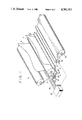
- FIG. 1 is a schematic perspective view of a printer provided with an electroconductive device according to the invention
- FIG. 2 is a partial perspective view illustrating an exploded printing head portion of FIG. 1,
- FIG. 3 is an explanatory structural view of an anisotropic electroconductive element made of resin
- FIG. 4 is an explanatory view illustrating an electroconductive state in the printing operation of the printer in FIG. 1.
- the electroconductive printer is composed of a line-type electroconductive transfer head 1, a platen 7 for feeding forms 5 to the electroconductive transfer head 1 together with two feed rollers 2 and 3, an electroconductive transfer sheet 9 as the printing medium which is attached between the form 5 and the head 1, a return electrode roller 13 for snapping and transferring the sheet 9 together with a feed rubber roller 11, and an electronic control device 20 or the like for driving and controlling the transfer head 1.
- the transfer head 1 is disposed over the entire length of the platen along a printing line under the platen 7.
- the head 1 is composed of a substrate 24 whose proximal end is rotatably attached to a rotray shaft 22, and an anisotropic element 26 (described later) forming a main printing portion and which is fixed on the substrate 24 over the direction of width of the form. Moreover, the substrate 24 is biased by a spring 27 in the direction of the arrow A of FIG. 1 so that the element 26 is made to contact the transfer sheet 9 under pressure by a predetermined bias force.
- a plurality of driving ICs 28 are packaged on one surface of the substrate for conducting the electroconductive transfer.
- a multiplicity of pattern electrodes 29 are formed for feeding the current serving to conduct the electroconductive transfer to the element from each output of the driving IC 28. This arrangement is described in more detail with reference to FIG. 2.
- these pattern electrodes 29 are provided in a band-shaped manner along the printing line at intervals equal to the printing density from the driving IC 28 up to that portion on the substrate 24 where the element 26 is fixed. Furthermore, pairs of insulation masks 30a and 30b spaced apart from each other are applied on those pattern electrodes 29, covering the region illustrated by the oblique line in FIG. 2. These masks 30a and 30b extend perpendicularly to the pattern electrode 29, element 26. As a result of the pattern electrodes 29, only the rectangular region 29a corresponding to the printing dot is exposed along the direction of the printing line. Thus the printing dots with a rectangular form, which form the printing pixels, are densely formed over the entire printing line.
- the element 26 is fixed to enable its release by a fixture (not shown), so that an end surface 26a extending along the direction of its thickness may contact the exposed region 29a of those electrode patterns 29.
- the element 26 is replaceable it may be completely fixed to the substrate 24.
- the arrangement in which the element 26 is attached to enable replacement has an advantage in that replacement work can easily be conducted when the element 26 undergoes wear or the like.
- the element 26, as shown in FIG. 3, is made of anisotropic electroconductive rubber materials which are embedded in great numbers with fine metallic fibers 31 aligned in their directions, and the direction of thickness, i.e. the direction of the arrow C, and exhibits excellent condcutivity while exhibiting a high insulation in the traverse direction.
- the surface 26b of the element 26 at the side contacting the transfer sheet 9 allows electrical conduction to the transfer sheet 9 over only the region in which the surface 26a at the reverse side is taken in the direction of the thickness.
- the printing pattern of the electrodes 29 which is electrically represented in the pattern region 29a corresponding to the printing dots through the turn-on surface 26a of the element 26 is transmitted as it is through the interior of the element to the other turn-on surface 26b through which the pattern is transmitted to the contacting transfer sheet 9.
- the electronic control device 20 supplies the control signal and the driving power through a flexible print circuit 33 to the driving IC 28 on the substrate 24, which controls the electrical conduction to each pattern electrode 29.
- electrical conduction is achieved through the transfer sheet 9 through the element 26, and thereby the printing operation by the electroconductive transfer is achieved.
- Transfer sheet 9 is the printing medium, as shown in FIG. 4, and is composed of an electrical resistance layer 9a, return layer 9b, and an ink layer 9c, and when the electrical conduction from the head 1 is achieved, the current I, as indicated by the arrows B, flows through the driving IC 28, pattern electrodes 29, element 26, resistance layer 9a, return layer 9b, and return electrodes roller 13.
- the resistance layer 9a having a resistance value R, instantaneously emits heat in accordance with the printing pattern and melts the corresponding region of the ink layer 9c to transfer the ink to the form 5.
- the electrode roller 13 is made of an excellent conductor, for example, metallic roller. Since it is pressed to the rubber roller 11, sharp projections provided along the periphery thereof contact the return layer 9b through the electric layer 9a. As a result, the return electrode roller 13 serves as the return electrode which passes current I not through the resistance layer 9a.
- the transfer sheet for example, the form for electroconductive printing may be used, and the printing element made of anisotropic electroconductive rubber in which metallic particles are dispersed in a specified direction of conduction, or made of anisotropic electroconductive resin may be used, and further a shuttle type of electroconductive print-head may be used.
Abstract
Description
Claims (8)
Applications Claiming Priority (2)
| Application Number | Priority Date | Filing Date | Title |
|---|---|---|---|
| JP61-62502 | 1986-03-19 | ||
| JP61062502A JPS62218153A (en) | 1986-03-19 | 1986-03-19 | Power conduction printing head |
Publications (1)
| Publication Number | Publication Date |
|---|---|
| US4781113A true US4781113A (en) | 1988-11-01 |
Family
ID=13202005
Family Applications (1)
| Application Number | Title | Priority Date | Filing Date |
|---|---|---|---|
| US07/028,090 Expired - Lifetime US4781113A (en) | 1986-03-19 | 1987-03-19 | Electric conduction printer |
Country Status (2)
| Country | Link |
|---|---|
| US (1) | US4781113A (en) |
| JP (1) | JPS62218153A (en) |
Cited By (5)
| Publication number | Priority date | Publication date | Assignee | Title |
|---|---|---|---|---|
| US4878772A (en) * | 1987-08-08 | 1989-11-07 | Mitsubishi Denki Kabushiki Kaisha | Thermal transcription printer |
| US5063394A (en) * | 1988-07-26 | 1991-11-05 | Kabushiki Kaisha Toshiba | Thermal recording apparatus and print head |
| GB2251214A (en) * | 1990-12-27 | 1992-07-01 | Brother Ind Ltd | Lithographic hand-stamp, and method of making it |
| EP0500334A2 (en) * | 1991-02-21 | 1992-08-26 | Riso Kagaku Corporation | Dot-matrix thermal recording device |
| US5357269A (en) * | 1992-06-01 | 1994-10-18 | Eastman Kodak Company | Electrical print head for thermal printer |
Citations (9)
| Publication number | Priority date | Publication date | Assignee | Title |
|---|---|---|---|---|
| US3719261A (en) * | 1969-11-12 | 1973-03-06 | Battelle Memorial Institute | Printing method and apparatus using conductive fusible ink |
| US3771634A (en) * | 1971-05-06 | 1973-11-13 | Bausch & Lomb | Surface pattern stylus board |
| US4023184A (en) * | 1975-10-06 | 1977-05-10 | Mfe Corporation | Thermal matrix type printing head |
| US4163075A (en) * | 1976-07-08 | 1979-07-31 | Sekisui Kagaku Kogyo Kabushiki Kaisha | Electric discharge recording material |
| US4425569A (en) * | 1981-05-19 | 1984-01-10 | Ricoh Company, Ltd. | Non-impact recording method and apparatus |
| US4461586A (en) * | 1981-05-20 | 1984-07-24 | Ricoh Company, Ltd. | Ink ribbon for use in electrothermic non-impact recording |
| US4636812A (en) * | 1985-10-24 | 1987-01-13 | Dynamics Research Corporation | Thermal print head temperature control |
| US4672391A (en) * | 1984-04-16 | 1987-06-09 | Hitachi, Ltd. | Thermal head |
| US4678701A (en) * | 1985-10-31 | 1987-07-07 | International Business Machines Corporation | Resistive printing ribbon having improved properties |
-
1986
- 1986-03-19 JP JP61062502A patent/JPS62218153A/en active Pending
-
1987
- 1987-03-19 US US07/028,090 patent/US4781113A/en not_active Expired - Lifetime
Patent Citations (9)
| Publication number | Priority date | Publication date | Assignee | Title |
|---|---|---|---|---|
| US3719261A (en) * | 1969-11-12 | 1973-03-06 | Battelle Memorial Institute | Printing method and apparatus using conductive fusible ink |
| US3771634A (en) * | 1971-05-06 | 1973-11-13 | Bausch & Lomb | Surface pattern stylus board |
| US4023184A (en) * | 1975-10-06 | 1977-05-10 | Mfe Corporation | Thermal matrix type printing head |
| US4163075A (en) * | 1976-07-08 | 1979-07-31 | Sekisui Kagaku Kogyo Kabushiki Kaisha | Electric discharge recording material |
| US4425569A (en) * | 1981-05-19 | 1984-01-10 | Ricoh Company, Ltd. | Non-impact recording method and apparatus |
| US4461586A (en) * | 1981-05-20 | 1984-07-24 | Ricoh Company, Ltd. | Ink ribbon for use in electrothermic non-impact recording |
| US4672391A (en) * | 1984-04-16 | 1987-06-09 | Hitachi, Ltd. | Thermal head |
| US4636812A (en) * | 1985-10-24 | 1987-01-13 | Dynamics Research Corporation | Thermal print head temperature control |
| US4678701A (en) * | 1985-10-31 | 1987-07-07 | International Business Machines Corporation | Resistive printing ribbon having improved properties |
Cited By (6)
| Publication number | Priority date | Publication date | Assignee | Title |
|---|---|---|---|---|
| US4878772A (en) * | 1987-08-08 | 1989-11-07 | Mitsubishi Denki Kabushiki Kaisha | Thermal transcription printer |
| US5063394A (en) * | 1988-07-26 | 1991-11-05 | Kabushiki Kaisha Toshiba | Thermal recording apparatus and print head |
| GB2251214A (en) * | 1990-12-27 | 1992-07-01 | Brother Ind Ltd | Lithographic hand-stamp, and method of making it |
| EP0500334A2 (en) * | 1991-02-21 | 1992-08-26 | Riso Kagaku Corporation | Dot-matrix thermal recording device |
| EP0500334A3 (en) * | 1991-02-21 | 1992-11-19 | Riso Kagaku Corporation | Dot-matrix thermal recording device |
| US5357269A (en) * | 1992-06-01 | 1994-10-18 | Eastman Kodak Company | Electrical print head for thermal printer |
Also Published As
| Publication number | Publication date |
|---|---|
| JPS62218153A (en) | 1987-09-25 |
Similar Documents
| Publication | Publication Date | Title |
|---|---|---|
| US3744611A (en) | Electro-thermic printing device | |
| JPS6160782B2 (en) | ||
| US4897668A (en) | Apparatus for transferring ink from ink ribbon to a recording medium by applying heat to the medium, thereby recording data on the medium | |
| US6879333B2 (en) | Resistive ribbon thermal print head and printer using the same | |
| US4781113A (en) | Electric conduction printer | |
| US4130752A (en) | Electrothermal print head | |
| US5170187A (en) | Ink supply mechanism for a thermal ink-jet recording apparatus | |
| US4855757A (en) | Thermal printhead with static electricity discharge capability | |
| JPH0263063B2 (en) | ||
| US6326990B1 (en) | Thick film thermal head and method of manufacturing the same | |
| JPS60174664A (en) | Recording head | |
| US4055743A (en) | Electrothermal print head | |
| EP0067953B1 (en) | Electrothermal printing apparatus | |
| EP0301891A1 (en) | Electrothermal printer with a resistive ink ribbon | |
| JP2012206267A (en) | Thermal head and thermal printer | |
| JPS62238766A (en) | Electrothermal head | |
| EP0288844B1 (en) | Recording head for use in an electrically excited transfer recording device | |
| US7057143B2 (en) | Fixing heater and image fixing apparatus incorporating the same | |
| JP3701749B2 (en) | printer | |
| CN112805153B (en) | Thermal head and thermal printer | |
| US4896977A (en) | Thermal printer having a structure for supporting a print head with a driver on its front surface | |
| US5023627A (en) | Printing head | |
| JPS57193386A (en) | Printer | |
| JPS6021293A (en) | Printing apparatus | |
| JPS63132064A (en) | Electrode head for current supply recording apparatus |
Legal Events
| Date | Code | Title | Description |
|---|---|---|---|
| AS | Assignment |
Owner name: BROTHER KOGYO KABUSHIKI KAISHA, 9-35, HORITADORI, Free format text: ASSIGNMENT OF ASSIGNORS INTEREST.;ASSIGNORS:YAMAMOTO, TAKEMI;KOBAYASHI, MASANORI;KIMURA, YASUO;REEL/FRAME:004715/0644;SIGNING DATES FROM 19870316 TO 19870317 Owner name: BROTHER KOGYO KABUSHIKI KAISHA, JAPAN Free format text: ASSIGNMENT OF ASSIGNORS INTEREST;ASSIGNORS:YAMAMOTO, TAKEMI;KOBAYASHI, MASANORI;KIMURA, YASUO;SIGNING DATES FROM 19870316 TO 19870317;REEL/FRAME:004715/0644 |
|
| STCF | Information on status: patent grant |
Free format text: PATENTED CASE |
|
| FEPP | Fee payment procedure |
Free format text: PAYOR NUMBER ASSIGNED (ORIGINAL EVENT CODE: ASPN); ENTITY STATUS OF PATENT OWNER: LARGE ENTITY |
|
| FEPP | Fee payment procedure |
Free format text: PAYOR NUMBER ASSIGNED (ORIGINAL EVENT CODE: ASPN); ENTITY STATUS OF PATENT OWNER: LARGE ENTITY Free format text: PAYER NUMBER DE-ASSIGNED (ORIGINAL EVENT CODE: RMPN); ENTITY STATUS OF PATENT OWNER: LARGE ENTITY |
|
| FPAY | Fee payment |
Year of fee payment: 4 |
|
| FPAY | Fee payment |
Year of fee payment: 8 |
|
| FPAY | Fee payment |
Year of fee payment: 12 |