US4737408A - Magneto-optical recording medium having plasma-polymerized protective layers - Google Patents
Magneto-optical recording medium having plasma-polymerized protective layers Download PDFInfo
- Publication number
- US4737408A US4737408A US06/897,087 US89708786A US4737408A US 4737408 A US4737408 A US 4737408A US 89708786 A US89708786 A US 89708786A US 4737408 A US4737408 A US 4737408A
- Authority
- US
- United States
- Prior art keywords
- plasma
- layer
- magneto
- recording medium
- optical recording
- Prior art date
- Legal status (The legal status is an assumption and is not a legal conclusion. Google has not performed a legal analysis and makes no representation as to the accuracy of the status listed.)
- Expired - Lifetime
Links
- 239000011241 protective layer Substances 0.000 title claims abstract description 69
- 239000010410 layer Substances 0.000 claims abstract description 127
- 239000010408 film Substances 0.000 claims abstract description 107
- 239000000758 substrate Substances 0.000 claims abstract description 89
- 239000010409 thin film Substances 0.000 claims abstract description 48
- 150000001875 compounds Chemical class 0.000 claims abstract description 27
- 238000000576 coating method Methods 0.000 claims abstract description 19
- 239000011248 coating agent Substances 0.000 claims abstract description 16
- 229910052761 rare earth metal Inorganic materials 0.000 claims abstract description 13
- 229910052723 transition metal Inorganic materials 0.000 claims abstract description 13
- 229910045601 alloy Inorganic materials 0.000 claims abstract description 9
- 239000000956 alloy Substances 0.000 claims abstract description 9
- 150000002910 rare earth metals Chemical class 0.000 claims abstract description 9
- 229910052799 carbon Inorganic materials 0.000 claims description 29
- OKTJSMMVPCPJKN-UHFFFAOYSA-N Carbon Chemical compound [C] OKTJSMMVPCPJKN-UHFFFAOYSA-N 0.000 claims description 26
- 230000005855 radiation Effects 0.000 claims description 22
- IJGRMHOSHXDMSA-UHFFFAOYSA-N Atomic nitrogen Chemical compound N#N IJGRMHOSHXDMSA-UHFFFAOYSA-N 0.000 claims description 16
- 229910052739 hydrogen Inorganic materials 0.000 claims description 15
- 229910052757 nitrogen Inorganic materials 0.000 claims description 14
- 125000004429 atom Chemical group 0.000 claims description 10
- 239000001257 hydrogen Substances 0.000 claims description 9
- QVGXLLKOCUKJST-UHFFFAOYSA-N atomic oxygen Chemical compound [O] QVGXLLKOCUKJST-UHFFFAOYSA-N 0.000 claims description 8
- 239000001301 oxygen Substances 0.000 claims description 8
- 229910052760 oxygen Inorganic materials 0.000 claims description 8
- 229910001872 inorganic gas Inorganic materials 0.000 claims description 4
- 150000004767 nitrides Chemical class 0.000 claims description 2
- 125000004435 hydrogen atom Chemical class [H]* 0.000 claims 5
- 239000007789 gas Substances 0.000 description 26
- 229920005989 resin Polymers 0.000 description 19
- 239000011347 resin Substances 0.000 description 19
- 239000000203 mixture Substances 0.000 description 18
- 239000000463 material Substances 0.000 description 13
- -1 MnAlGe Inorganic materials 0.000 description 12
- 238000006116 polymerization reaction Methods 0.000 description 10
- 239000011247 coating layer Substances 0.000 description 8
- 238000009832 plasma treatment Methods 0.000 description 8
- VYPSYNLAJGMNEJ-UHFFFAOYSA-N Silicium dioxide Chemical compound O=[Si]=O VYPSYNLAJGMNEJ-UHFFFAOYSA-N 0.000 description 7
- 238000000034 method Methods 0.000 description 7
- 238000004544 sputter deposition Methods 0.000 description 7
- 238000003860 storage Methods 0.000 description 7
- 230000003287 optical effect Effects 0.000 description 6
- 230000001681 protective effect Effects 0.000 description 6
- 238000001004 secondary ion mass spectrometry Methods 0.000 description 6
- 230000008859 change Effects 0.000 description 5
- WXZMFSXDPGVJKK-UHFFFAOYSA-N pentaerythritol Chemical compound OCC(CO)(CO)CO WXZMFSXDPGVJKK-UHFFFAOYSA-N 0.000 description 5
- 229920005992 thermoplastic resin Polymers 0.000 description 5
- 239000004215 Carbon black (E152) Substances 0.000 description 4
- CERQOIWHTDAKMF-UHFFFAOYSA-M Methacrylate Chemical compound CC(=C)C([O-])=O CERQOIWHTDAKMF-UHFFFAOYSA-M 0.000 description 4
- 230000008901 benefit Effects 0.000 description 4
- 239000008199 coating composition Substances 0.000 description 4
- 238000004132 cross linking Methods 0.000 description 4
- 230000006866 deterioration Effects 0.000 description 4
- 229930195733 hydrocarbon Natural products 0.000 description 4
- 150000002430 hydrocarbons Chemical class 0.000 description 4
- 230000006872 improvement Effects 0.000 description 4
- 229910010272 inorganic material Inorganic materials 0.000 description 4
- 239000011147 inorganic material Substances 0.000 description 4
- 230000005415 magnetization Effects 0.000 description 4
- 230000008569 process Effects 0.000 description 4
- LIVNPJMFVYWSIS-UHFFFAOYSA-N silicon monoxide Chemical compound [Si-]#[O+] LIVNPJMFVYWSIS-UHFFFAOYSA-N 0.000 description 4
- 150000003624 transition metals Chemical class 0.000 description 4
- 238000001771 vacuum deposition Methods 0.000 description 4
- UFHFLCQGNIYNRP-UHFFFAOYSA-N Hydrogen Chemical compound [H][H] UFHFLCQGNIYNRP-UHFFFAOYSA-N 0.000 description 3
- 150000001252 acrylic acid derivatives Chemical class 0.000 description 3
- 239000000853 adhesive Substances 0.000 description 3
- 230000001070 adhesive effect Effects 0.000 description 3
- 238000013459 approach Methods 0.000 description 3
- 238000006243 chemical reaction Methods 0.000 description 3
- 230000000052 comparative effect Effects 0.000 description 3
- 238000010276 construction Methods 0.000 description 3
- 230000005684 electric field Effects 0.000 description 3
- 239000003822 epoxy resin Substances 0.000 description 3
- 150000002148 esters Chemical class 0.000 description 3
- 239000011521 glass Substances 0.000 description 3
- 238000005259 measurement Methods 0.000 description 3
- 125000005395 methacrylic acid group Chemical class 0.000 description 3
- 239000000178 monomer Substances 0.000 description 3
- OFBQJSOFQDEBGM-UHFFFAOYSA-N n-pentane Natural products CCCCC OFBQJSOFQDEBGM-UHFFFAOYSA-N 0.000 description 3
- 229920003229 poly(methyl methacrylate) Polymers 0.000 description 3
- 229920000647 polyepoxide Polymers 0.000 description 3
- 239000004926 polymethyl methacrylate Substances 0.000 description 3
- 239000012260 resinous material Substances 0.000 description 3
- 239000000377 silicon dioxide Substances 0.000 description 3
- XFCMNSHQOZQILR-UHFFFAOYSA-N 2-[2-(2-methylprop-2-enoyloxy)ethoxy]ethyl 2-methylprop-2-enoate Chemical compound CC(=C)C(=O)OCCOCCOC(=O)C(C)=C XFCMNSHQOZQILR-UHFFFAOYSA-N 0.000 description 2
- KUDUQBURMYMBIJ-UHFFFAOYSA-N 2-prop-2-enoyloxyethyl prop-2-enoate Chemical compound C=CC(=O)OCCOC(=O)C=C KUDUQBURMYMBIJ-UHFFFAOYSA-N 0.000 description 2
- KWOLFJPFCHCOCG-UHFFFAOYSA-N Acetophenone Chemical compound CC(=O)C1=CC=CC=C1 KWOLFJPFCHCOCG-UHFFFAOYSA-N 0.000 description 2
- 229920000178 Acrylic resin Polymers 0.000 description 2
- 239000004925 Acrylic resin Substances 0.000 description 2
- XKRFYHLGVUSROY-UHFFFAOYSA-N Argon Chemical compound [Ar] XKRFYHLGVUSROY-UHFFFAOYSA-N 0.000 description 2
- KAKZBPTYRLMSJV-UHFFFAOYSA-N Butadiene Chemical compound C=CC=C KAKZBPTYRLMSJV-UHFFFAOYSA-N 0.000 description 2
- 239000004641 Diallyl-phthalate Substances 0.000 description 2
- 206010073306 Exposure to radiation Diseases 0.000 description 2
- XEEYBQQBJWHFJM-UHFFFAOYSA-N Iron Chemical compound [Fe] XEEYBQQBJWHFJM-UHFFFAOYSA-N 0.000 description 2
- 239000004372 Polyvinyl alcohol Substances 0.000 description 2
- ATUOYWHBWRKTHZ-UHFFFAOYSA-N Propane Chemical compound CCC ATUOYWHBWRKTHZ-UHFFFAOYSA-N 0.000 description 2
- OFOBLEOULBTSOW-UHFFFAOYSA-N Propanedioic acid Natural products OC(=O)CC(O)=O OFOBLEOULBTSOW-UHFFFAOYSA-N 0.000 description 2
- 229910007277 Si3 N4 Inorganic materials 0.000 description 2
- 229910052581 Si3N4 Inorganic materials 0.000 description 2
- PPBRXRYQALVLMV-UHFFFAOYSA-N Styrene Chemical compound C=CC1=CC=CC=C1 PPBRXRYQALVLMV-UHFFFAOYSA-N 0.000 description 2
- 229910052771 Terbium Inorganic materials 0.000 description 2
- 229920006311 Urethane elastomer Polymers 0.000 description 2
- XLOMVQKBTHCTTD-UHFFFAOYSA-N Zinc monoxide Chemical compound [Zn]=O XLOMVQKBTHCTTD-UHFFFAOYSA-N 0.000 description 2
- NIXOWILDQLNWCW-UHFFFAOYSA-N acrylic acid group Chemical group C(C=C)(=O)O NIXOWILDQLNWCW-UHFFFAOYSA-N 0.000 description 2
- 229910052786 argon Inorganic materials 0.000 description 2
- 239000012965 benzophenone Substances 0.000 description 2
- 230000015572 biosynthetic process Effects 0.000 description 2
- QUDWYFHPNIMBFC-UHFFFAOYSA-N bis(prop-2-enyl) benzene-1,2-dicarboxylate Chemical compound C=CCOC(=O)C1=CC=CC=C1C(=O)OCC=C QUDWYFHPNIMBFC-UHFFFAOYSA-N 0.000 description 2
- 239000012159 carrier gas Substances 0.000 description 2
- 239000013626 chemical specie Substances 0.000 description 2
- 229910052681 coesite Inorganic materials 0.000 description 2
- 229910052906 cristobalite Inorganic materials 0.000 description 2
- 230000000694 effects Effects 0.000 description 2
- 125000000524 functional group Chemical group 0.000 description 2
- 238000007756 gravure coating Methods 0.000 description 2
- LNEPOXFFQSENCJ-UHFFFAOYSA-N haloperidol Chemical compound C1CC(O)(C=2C=CC(Cl)=CC=2)CCN1CCCC(=O)C1=CC=C(F)C=C1 LNEPOXFFQSENCJ-UHFFFAOYSA-N 0.000 description 2
- 239000012943 hotmelt Substances 0.000 description 2
- VZCYOOQTPOCHFL-UPHRSURJSA-N maleic acid Chemical compound OC(=O)\C=C/C(O)=O VZCYOOQTPOCHFL-UPHRSURJSA-N 0.000 description 2
- 239000011976 maleic acid Substances 0.000 description 2
- VNWKTOKETHGBQD-UHFFFAOYSA-N methane Chemical compound C VNWKTOKETHGBQD-UHFFFAOYSA-N 0.000 description 2
- 125000000896 monocarboxylic acid group Chemical group 0.000 description 2
- 239000003921 oil Substances 0.000 description 2
- 239000005011 phenolic resin Substances 0.000 description 2
- 239000003504 photosensitizing agent Substances 0.000 description 2
- 229920001225 polyester resin Polymers 0.000 description 2
- 239000004645 polyester resin Substances 0.000 description 2
- 229920000642 polymer Polymers 0.000 description 2
- 230000000379 polymerizing effect Effects 0.000 description 2
- 229920002635 polyurethane Polymers 0.000 description 2
- 239000004814 polyurethane Substances 0.000 description 2
- 229920002451 polyvinyl alcohol Polymers 0.000 description 2
- 238000010526 radical polymerization reaction Methods 0.000 description 2
- 229920006395 saturated elastomer Polymers 0.000 description 2
- HQVNEWCFYHHQES-UHFFFAOYSA-N silicon nitride Chemical compound N12[Si]34N5[Si]62N3[Si]51N64 HQVNEWCFYHHQES-UHFFFAOYSA-N 0.000 description 2
- 238000005507 spraying Methods 0.000 description 2
- 229910052682 stishovite Inorganic materials 0.000 description 2
- 229920001187 thermosetting polymer Polymers 0.000 description 2
- VZCYOOQTPOCHFL-UHFFFAOYSA-N trans-butenedioic acid Natural products OC(=O)C=CC(O)=O VZCYOOQTPOCHFL-UHFFFAOYSA-N 0.000 description 2
- 229910052905 tridymite Inorganic materials 0.000 description 2
- MYWOJODOMFBVCB-UHFFFAOYSA-N 1,2,6-trimethylphenanthrene Chemical compound CC1=CC=C2C3=CC(C)=CC=C3C=CC2=C1C MYWOJODOMFBVCB-UHFFFAOYSA-N 0.000 description 1
- RWXMAAYKJDQVTF-UHFFFAOYSA-N 2-(2-hydroxyethoxy)ethyl prop-2-enoate Chemical compound OCCOCCOC(=O)C=C RWXMAAYKJDQVTF-UHFFFAOYSA-N 0.000 description 1
- RXDYOLRABMJTEF-UHFFFAOYSA-N 2-chloro-1,2-diphenylethanone Chemical compound C=1C=CC=CC=1C(Cl)C(=O)C1=CC=CC=C1 RXDYOLRABMJTEF-UHFFFAOYSA-N 0.000 description 1
- KMNCBSZOIQAUFX-UHFFFAOYSA-N 2-ethoxy-1,2-diphenylethanone Chemical compound C=1C=CC=CC=1C(OCC)C(=O)C1=CC=CC=C1 KMNCBSZOIQAUFX-UHFFFAOYSA-N 0.000 description 1
- DIVXVZXROTWKIH-UHFFFAOYSA-N 2-hydroxy-1,2-diphenylpropan-1-one Chemical compound C=1C=CC=CC=1C(O)(C)C(=O)C1=CC=CC=C1 DIVXVZXROTWKIH-UHFFFAOYSA-N 0.000 description 1
- BQZJOQXSCSZQPS-UHFFFAOYSA-N 2-methoxy-1,2-diphenylethanone Chemical compound C=1C=CC=CC=1C(OC)C(=O)C1=CC=CC=C1 BQZJOQXSCSZQPS-UHFFFAOYSA-N 0.000 description 1
- BUZICZZQJDLXJN-UHFFFAOYSA-N 3-azaniumyl-4-hydroxybutanoate Chemical compound OCC(N)CC(O)=O BUZICZZQJDLXJN-UHFFFAOYSA-N 0.000 description 1
- DBCAQXHNJOFNGC-UHFFFAOYSA-N 4-bromo-1,1,1-trifluorobutane Chemical compound FC(F)(F)CCCBr DBCAQXHNJOFNGC-UHFFFAOYSA-N 0.000 description 1
- YYVYAPXYZVYDHN-UHFFFAOYSA-N 9,10-phenanthroquinone Chemical compound C1=CC=C2C(=O)C(=O)C3=CC=CC=C3C2=C1 YYVYAPXYZVYDHN-UHFFFAOYSA-N 0.000 description 1
- NIXOWILDQLNWCW-UHFFFAOYSA-M Acrylate Chemical compound [O-]C(=O)C=C NIXOWILDQLNWCW-UHFFFAOYSA-M 0.000 description 1
- 229910017083 AlN Inorganic materials 0.000 description 1
- PIGFYZPCRLYGLF-UHFFFAOYSA-N Aluminum nitride Chemical compound [Al]#N PIGFYZPCRLYGLF-UHFFFAOYSA-N 0.000 description 1
- 229910052582 BN Inorganic materials 0.000 description 1
- ZOXJGFHDIHLPTG-UHFFFAOYSA-N Boron Chemical compound [B] ZOXJGFHDIHLPTG-UHFFFAOYSA-N 0.000 description 1
- PZNSFCLAULLKQX-UHFFFAOYSA-N Boron nitride Chemical compound N#B PZNSFCLAULLKQX-UHFFFAOYSA-N 0.000 description 1
- WLENCUMVFNNMBU-UHFFFAOYSA-N C1CO1.C1(=CC=CC=C1)O.C(C(=C)C)(=O)O.C(C=C)(=O)O.C(C=C)(=O)O.C(O)C(CC)(CO)CO Chemical class C1CO1.C1(=CC=CC=C1)O.C(C(=C)C)(=O)O.C(C=C)(=O)O.C(C=C)(=O)O.C(O)C(CC)(CO)CO WLENCUMVFNNMBU-UHFFFAOYSA-N 0.000 description 1
- 229920000089 Cyclic olefin copolymer Polymers 0.000 description 1
- OTMSDBZUPAUEDD-UHFFFAOYSA-N Ethane Chemical compound CC OTMSDBZUPAUEDD-UHFFFAOYSA-N 0.000 description 1
- JIGUQPWFLRLWPJ-UHFFFAOYSA-N Ethyl acrylate Chemical compound CCOC(=O)C=C JIGUQPWFLRLWPJ-UHFFFAOYSA-N 0.000 description 1
- YCKRFDGAMUMZLT-UHFFFAOYSA-N Fluorine atom Chemical compound [F] YCKRFDGAMUMZLT-UHFFFAOYSA-N 0.000 description 1
- 229910052688 Gadolinium Inorganic materials 0.000 description 1
- 229920000877 Melamine resin Polymers 0.000 description 1
- 229910016629 MnBi Inorganic materials 0.000 description 1
- 229910016964 MnSb Inorganic materials 0.000 description 1
- OAICVXFJPJFONN-UHFFFAOYSA-N Phosphorus Chemical compound [P] OAICVXFJPJFONN-UHFFFAOYSA-N 0.000 description 1
- 239000004952 Polyamide Substances 0.000 description 1
- 239000004698 Polyethylene Substances 0.000 description 1
- 239000004721 Polyphenylene oxide Substances 0.000 description 1
- 239000004743 Polypropylene Substances 0.000 description 1
- 239000004793 Polystyrene Substances 0.000 description 1
- 229920001328 Polyvinylidene chloride Polymers 0.000 description 1
- 229910002837 PtCo Inorganic materials 0.000 description 1
- 101100386054 Saccharomyces cerevisiae (strain ATCC 204508 / S288c) CYS3 gene Proteins 0.000 description 1
- XUIMIQQOPSSXEZ-UHFFFAOYSA-N Silicon Chemical compound [Si] XUIMIQQOPSSXEZ-UHFFFAOYSA-N 0.000 description 1
- 235000000126 Styrax benzoin Nutrition 0.000 description 1
- 244000028419 Styrax benzoin Species 0.000 description 1
- NINIDFKCEFEMDL-UHFFFAOYSA-N Sulfur Chemical compound [S] NINIDFKCEFEMDL-UHFFFAOYSA-N 0.000 description 1
- 235000008411 Sumatra benzointree Nutrition 0.000 description 1
- GWEVSGVZZGPLCZ-UHFFFAOYSA-N Titan oxide Chemical compound O=[Ti]=O GWEVSGVZZGPLCZ-UHFFFAOYSA-N 0.000 description 1
- NRTOMJZYCJJWKI-UHFFFAOYSA-N Titanium nitride Chemical compound [Ti]#N NRTOMJZYCJJWKI-UHFFFAOYSA-N 0.000 description 1
- ZJCCRDAZUWHFQH-UHFFFAOYSA-N Trimethylolpropane Chemical compound CCC(CO)(CO)CO ZJCCRDAZUWHFQH-UHFFFAOYSA-N 0.000 description 1
- DAKWPKUUDNSNPN-UHFFFAOYSA-N Trimethylolpropane triacrylate Chemical compound C=CC(=O)OCC(CC)(COC(=O)C=C)COC(=O)C=C DAKWPKUUDNSNPN-UHFFFAOYSA-N 0.000 description 1
- 229920001807 Urea-formaldehyde Polymers 0.000 description 1
- HVVWZTWDBSEWIH-UHFFFAOYSA-N [2-(hydroxymethyl)-3-prop-2-enoyloxy-2-(prop-2-enoyloxymethyl)propyl] prop-2-enoate Chemical compound C=CC(=O)OCC(CO)(COC(=O)C=C)COC(=O)C=C HVVWZTWDBSEWIH-UHFFFAOYSA-N 0.000 description 1
- 239000000654 additive Substances 0.000 description 1
- 230000000996 additive effect Effects 0.000 description 1
- 230000001464 adherent effect Effects 0.000 description 1
- 239000002390 adhesive tape Substances 0.000 description 1
- 229920000180 alkyd Polymers 0.000 description 1
- 125000000217 alkyl group Chemical group 0.000 description 1
- HSFWRNGVRCDJHI-UHFFFAOYSA-N alpha-acetylene Natural products C#C HSFWRNGVRCDJHI-UHFFFAOYSA-N 0.000 description 1
- PYKYMHQGRFAEBM-UHFFFAOYSA-N anthraquinone Natural products CCC(=O)c1c(O)c2C(=O)C3C(C=CC=C3O)C(=O)c2cc1CC(=O)OC PYKYMHQGRFAEBM-UHFFFAOYSA-N 0.000 description 1
- 150000004056 anthraquinones Chemical class 0.000 description 1
- 238000004774 atomic orbital Methods 0.000 description 1
- WPYMKLBDIGXBTP-UHFFFAOYSA-N benzoic acid Chemical compound OC(=O)C1=CC=CC=C1 WPYMKLBDIGXBTP-UHFFFAOYSA-N 0.000 description 1
- RWCCWEUUXYIKHB-UHFFFAOYSA-N benzophenone Chemical compound C=1C=CC=CC=1C(=O)C1=CC=CC=C1 RWCCWEUUXYIKHB-UHFFFAOYSA-N 0.000 description 1
- 150000008366 benzophenones Chemical class 0.000 description 1
- LUFPJJNWMYZRQE-UHFFFAOYSA-N benzylsulfanylmethylbenzene Chemical compound C=1C=CC=CC=1CSCC1=CC=CC=C1 LUFPJJNWMYZRQE-UHFFFAOYSA-N 0.000 description 1
- 230000008033 biological extinction Effects 0.000 description 1
- 229910052796 boron Inorganic materials 0.000 description 1
- 239000001273 butane Substances 0.000 description 1
- 239000000919 ceramic Substances 0.000 description 1
- 229910010293 ceramic material Inorganic materials 0.000 description 1
- 229910017052 cobalt Inorganic materials 0.000 description 1
- 239000010941 cobalt Substances 0.000 description 1
- GUTLYIVDDKVIGB-UHFFFAOYSA-N cobalt atom Chemical compound [Co] GUTLYIVDDKVIGB-UHFFFAOYSA-N 0.000 description 1
- 230000001276 controlling effect Effects 0.000 description 1
- 238000007796 conventional method Methods 0.000 description 1
- 229920001577 copolymer Polymers 0.000 description 1
- PMHQVHHXPFUNSP-UHFFFAOYSA-M copper(1+);methylsulfanylmethane;bromide Chemical compound Br[Cu].CSC PMHQVHHXPFUNSP-UHFFFAOYSA-M 0.000 description 1
- 230000002596 correlated effect Effects 0.000 description 1
- 230000007547 defect Effects 0.000 description 1
- 238000009792 diffusion process Methods 0.000 description 1
- 238000007598 dipping method Methods 0.000 description 1
- 230000005670 electromagnetic radiation Effects 0.000 description 1
- 238000000921 elemental analysis Methods 0.000 description 1
- STVZJERGLQHEKB-UHFFFAOYSA-N ethylene glycol dimethacrylate Substances CC(=C)C(=O)OCCOC(=O)C(C)=C STVZJERGLQHEKB-UHFFFAOYSA-N 0.000 description 1
- 125000002534 ethynyl group Chemical group [H]C#C* 0.000 description 1
- 239000011737 fluorine Substances 0.000 description 1
- 229910052731 fluorine Inorganic materials 0.000 description 1
- 238000009472 formulation Methods 0.000 description 1
- 239000003574 free electron Substances 0.000 description 1
- UIWYJDYFSGRHKR-UHFFFAOYSA-N gadolinium atom Chemical compound [Gd] UIWYJDYFSGRHKR-UHFFFAOYSA-N 0.000 description 1
- ZSOJHTHUCUGDHS-UHFFFAOYSA-N gadolinium iron Chemical compound [Fe].[Gd] ZSOJHTHUCUGDHS-UHFFFAOYSA-N 0.000 description 1
- 239000002223 garnet Substances 0.000 description 1
- 235000019382 gum benzoic Nutrition 0.000 description 1
- 150000002431 hydrogen Chemical class 0.000 description 1
- 125000002887 hydroxy group Chemical group [H]O* 0.000 description 1
- 238000010348 incorporation Methods 0.000 description 1
- 230000001939 inductive effect Effects 0.000 description 1
- 150000002500 ions Chemical class 0.000 description 1
- 150000002576 ketones Chemical class 0.000 description 1
- 238000000281 laser microprobe mass spectrometry Methods 0.000 description 1
- 239000007788 liquid Substances 0.000 description 1
- 230000007774 longterm Effects 0.000 description 1
- 238000004519 manufacturing process Methods 0.000 description 1
- 150000002734 metacrylic acid derivatives Chemical class 0.000 description 1
- 125000005641 methacryl group Chemical group 0.000 description 1
- 238000004776 molecular orbital Methods 0.000 description 1
- IJDNQMDRQITEOD-UHFFFAOYSA-N n-butane Chemical compound CCCC IJDNQMDRQITEOD-UHFFFAOYSA-N 0.000 description 1
- 230000007935 neutral effect Effects 0.000 description 1
- 229920002601 oligoester Polymers 0.000 description 1
- 239000011368 organic material Substances 0.000 description 1
- TWNQGVIAIRXVLR-UHFFFAOYSA-N oxo(oxoalumanyloxy)alumane Chemical compound O=[Al]O[Al]=O TWNQGVIAIRXVLR-UHFFFAOYSA-N 0.000 description 1
- 230000000149 penetrating effect Effects 0.000 description 1
- PNJWIWWMYCMZRO-UHFFFAOYSA-N pent‐4‐en‐2‐one Natural products CC(=O)CC=C PNJWIWWMYCMZRO-UHFFFAOYSA-N 0.000 description 1
- 230000002093 peripheral effect Effects 0.000 description 1
- 229920001568 phenolic resin Polymers 0.000 description 1
- 229920006287 phenoxy resin Polymers 0.000 description 1
- 239000013034 phenoxy resin Substances 0.000 description 1
- 229910052698 phosphorus Inorganic materials 0.000 description 1
- 239000011574 phosphorus Substances 0.000 description 1
- 229920003023 plastic Polymers 0.000 description 1
- 239000004033 plastic Substances 0.000 description 1
- 230000010287 polarization Effects 0.000 description 1
- 229920002647 polyamide Polymers 0.000 description 1
- 229920006122 polyamide resin Polymers 0.000 description 1
- 239000004417 polycarbonate Substances 0.000 description 1
- 229920000515 polycarbonate Polymers 0.000 description 1
- 229920005668 polycarbonate resin Polymers 0.000 description 1
- 239000004431 polycarbonate resin Substances 0.000 description 1
- 229920000570 polyether Polymers 0.000 description 1
- 229920000573 polyethylene Polymers 0.000 description 1
- 229920001721 polyimide Polymers 0.000 description 1
- 239000009719 polyimide resin Substances 0.000 description 1
- 229920000306 polymethylpentene Polymers 0.000 description 1
- 239000011116 polymethylpentene Substances 0.000 description 1
- 229920006324 polyoxymethylene Polymers 0.000 description 1
- 229920001155 polypropylene Polymers 0.000 description 1
- 229920002223 polystyrene Polymers 0.000 description 1
- 229920000915 polyvinyl chloride Polymers 0.000 description 1
- 239000004800 polyvinyl chloride Substances 0.000 description 1
- 239000005033 polyvinylidene chloride Substances 0.000 description 1
- 239000001267 polyvinylpyrrolidone Substances 0.000 description 1
- 229920000036 polyvinylpyrrolidone Polymers 0.000 description 1
- 235000013855 polyvinylpyrrolidone Nutrition 0.000 description 1
- 239000001294 propane Substances 0.000 description 1
- MWWATHDPGQKSAR-UHFFFAOYSA-N propyne Chemical group CC#C MWWATHDPGQKSAR-UHFFFAOYSA-N 0.000 description 1
- 150000004053 quinones Chemical class 0.000 description 1
- 230000035484 reaction time Effects 0.000 description 1
- 230000004044 response Effects 0.000 description 1
- 229930195734 saturated hydrocarbon Natural products 0.000 description 1
- 229910052710 silicon Inorganic materials 0.000 description 1
- 239000010703 silicon Substances 0.000 description 1
- 235000012239 silicon dioxide Nutrition 0.000 description 1
- 229910052814 silicon oxide Inorganic materials 0.000 description 1
- 229920002050 silicone resin Polymers 0.000 description 1
- 239000007787 solid Substances 0.000 description 1
- 229910052950 sphalerite Inorganic materials 0.000 description 1
- 238000000992 sputter etching Methods 0.000 description 1
- 101150035983 str1 gene Proteins 0.000 description 1
- 239000000126 substance Substances 0.000 description 1
- 229910052717 sulfur Inorganic materials 0.000 description 1
- 239000011593 sulfur Substances 0.000 description 1
- 238000005211 surface analysis Methods 0.000 description 1
- GZCRRIHWUXGPOV-UHFFFAOYSA-N terbium atom Chemical compound [Tb] GZCRRIHWUXGPOV-UHFFFAOYSA-N 0.000 description 1
- 150000003568 thioethers Chemical class 0.000 description 1
- OGIDPMRJRNCKJF-UHFFFAOYSA-N titanium oxide Inorganic materials [Ti]=O OGIDPMRJRNCKJF-UHFFFAOYSA-N 0.000 description 1
- 238000002834 transmittance Methods 0.000 description 1
- 229930195735 unsaturated hydrocarbon Natural products 0.000 description 1
- 229920006337 unsaturated polyester resin Polymers 0.000 description 1
- 150000003673 urethanes Chemical class 0.000 description 1
- 229910052724 xenon Inorganic materials 0.000 description 1
- FHNFHKCVQCLJFQ-UHFFFAOYSA-N xenon atom Chemical compound [Xe] FHNFHKCVQCLJFQ-UHFFFAOYSA-N 0.000 description 1
- 239000011787 zinc oxide Substances 0.000 description 1
- 229910052984 zinc sulfide Inorganic materials 0.000 description 1
Images


Classifications
-
- G—PHYSICS
- G11—INFORMATION STORAGE
- G11B—INFORMATION STORAGE BASED ON RELATIVE MOVEMENT BETWEEN RECORD CARRIER AND TRANSDUCER
- G11B7/00—Recording or reproducing by optical means, e.g. recording using a thermal beam of optical radiation by modifying optical properties or the physical structure, reproducing using an optical beam at lower power by sensing optical properties; Record carriers therefor
- G11B7/24—Record carriers characterised by shape, structure or physical properties, or by the selection of the material
- G11B7/241—Record carriers characterised by shape, structure or physical properties, or by the selection of the material characterised by the selection of the material
- G11B7/252—Record carriers characterised by shape, structure or physical properties, or by the selection of the material characterised by the selection of the material of layers other than recording layers
-
- G—PHYSICS
- G11—INFORMATION STORAGE
- G11B—INFORMATION STORAGE BASED ON RELATIVE MOVEMENT BETWEEN RECORD CARRIER AND TRANSDUCER
- G11B11/00—Recording on or reproducing from the same record carrier wherein for these two operations the methods are covered by different main groups of groups G11B3/00 - G11B7/00 or by different subgroups of group G11B9/00; Record carriers therefor
- G11B11/10—Recording on or reproducing from the same record carrier wherein for these two operations the methods are covered by different main groups of groups G11B3/00 - G11B7/00 or by different subgroups of group G11B9/00; Record carriers therefor using recording by magnetic means or other means for magnetisation or demagnetisation of a record carrier, e.g. light induced spin magnetisation; Demagnetisation by thermal or stress means in the presence or not of an orienting magnetic field
- G11B11/105—Recording on or reproducing from the same record carrier wherein for these two operations the methods are covered by different main groups of groups G11B3/00 - G11B7/00 or by different subgroups of group G11B9/00; Record carriers therefor using recording by magnetic means or other means for magnetisation or demagnetisation of a record carrier, e.g. light induced spin magnetisation; Demagnetisation by thermal or stress means in the presence or not of an orienting magnetic field using a beam of light or a magnetic field for recording by change of magnetisation and a beam of light for reproducing, i.e. magneto-optical, e.g. light-induced thermomagnetic recording, spin magnetisation recording, Kerr or Faraday effect reproducing
- G11B11/10582—Record carriers characterised by the selection of the material or by the structure or form
-
- G—PHYSICS
- G11—INFORMATION STORAGE
- G11B—INFORMATION STORAGE BASED ON RELATIVE MOVEMENT BETWEEN RECORD CARRIER AND TRANSDUCER
- G11B7/00—Recording or reproducing by optical means, e.g. recording using a thermal beam of optical radiation by modifying optical properties or the physical structure, reproducing using an optical beam at lower power by sensing optical properties; Record carriers therefor
- G11B7/24—Record carriers characterised by shape, structure or physical properties, or by the selection of the material
- G11B7/241—Record carriers characterised by shape, structure or physical properties, or by the selection of the material characterised by the selection of the material
- G11B7/252—Record carriers characterised by shape, structure or physical properties, or by the selection of the material characterised by the selection of the material of layers other than recording layers
- G11B7/254—Record carriers characterised by shape, structure or physical properties, or by the selection of the material characterised by the selection of the material of layers other than recording layers of protective topcoat layers
-
- G—PHYSICS
- G11—INFORMATION STORAGE
- G11B—INFORMATION STORAGE BASED ON RELATIVE MOVEMENT BETWEEN RECORD CARRIER AND TRANSDUCER
- G11B7/00—Recording or reproducing by optical means, e.g. recording using a thermal beam of optical radiation by modifying optical properties or the physical structure, reproducing using an optical beam at lower power by sensing optical properties; Record carriers therefor
- G11B7/24—Record carriers characterised by shape, structure or physical properties, or by the selection of the material
- G11B7/241—Record carriers characterised by shape, structure or physical properties, or by the selection of the material characterised by the selection of the material
- G11B7/252—Record carriers characterised by shape, structure or physical properties, or by the selection of the material characterised by the selection of the material of layers other than recording layers
- G11B7/257—Record carriers characterised by shape, structure or physical properties, or by the selection of the material characterised by the selection of the material of layers other than recording layers of layers having properties involved in recording or reproduction, e.g. optical interference layers or sensitising layers or dielectric layers, which are protecting the recording layers
- G11B7/2572—Record carriers characterised by shape, structure or physical properties, or by the selection of the material characterised by the selection of the material of layers other than recording layers of layers having properties involved in recording or reproduction, e.g. optical interference layers or sensitising layers or dielectric layers, which are protecting the recording layers consisting essentially of organic materials
- G11B7/2575—Record carriers characterised by shape, structure or physical properties, or by the selection of the material characterised by the selection of the material of layers other than recording layers of layers having properties involved in recording or reproduction, e.g. optical interference layers or sensitising layers or dielectric layers, which are protecting the recording layers consisting essentially of organic materials resins
-
- G—PHYSICS
- G11—INFORMATION STORAGE
- G11B—INFORMATION STORAGE BASED ON RELATIVE MOVEMENT BETWEEN RECORD CARRIER AND TRANSDUCER
- G11B7/00—Recording or reproducing by optical means, e.g. recording using a thermal beam of optical radiation by modifying optical properties or the physical structure, reproducing using an optical beam at lower power by sensing optical properties; Record carriers therefor
- G11B7/24—Record carriers characterised by shape, structure or physical properties, or by the selection of the material
- G11B7/241—Record carriers characterised by shape, structure or physical properties, or by the selection of the material characterised by the selection of the material
- G11B7/242—Record carriers characterised by shape, structure or physical properties, or by the selection of the material characterised by the selection of the material of recording layers
- G11B7/243—Record carriers characterised by shape, structure or physical properties, or by the selection of the material characterised by the selection of the material of recording layers comprising inorganic materials only, e.g. ablative layers
- G11B2007/24302—Metals or metalloids
- G11B2007/24306—Metals or metalloids transition metal elements of groups 3-10
-
- G—PHYSICS
- G11—INFORMATION STORAGE
- G11B—INFORMATION STORAGE BASED ON RELATIVE MOVEMENT BETWEEN RECORD CARRIER AND TRANSDUCER
- G11B7/00—Recording or reproducing by optical means, e.g. recording using a thermal beam of optical radiation by modifying optical properties or the physical structure, reproducing using an optical beam at lower power by sensing optical properties; Record carriers therefor
- G11B7/24—Record carriers characterised by shape, structure or physical properties, or by the selection of the material
- G11B7/241—Record carriers characterised by shape, structure or physical properties, or by the selection of the material characterised by the selection of the material
- G11B7/252—Record carriers characterised by shape, structure or physical properties, or by the selection of the material characterised by the selection of the material of layers other than recording layers
- G11B7/253—Record carriers characterised by shape, structure or physical properties, or by the selection of the material characterised by the selection of the material of layers other than recording layers of substrates
- G11B7/2533—Record carriers characterised by shape, structure or physical properties, or by the selection of the material characterised by the selection of the material of layers other than recording layers of substrates comprising resins
-
- Y—GENERAL TAGGING OF NEW TECHNOLOGICAL DEVELOPMENTS; GENERAL TAGGING OF CROSS-SECTIONAL TECHNOLOGIES SPANNING OVER SEVERAL SECTIONS OF THE IPC; TECHNICAL SUBJECTS COVERED BY FORMER USPC CROSS-REFERENCE ART COLLECTIONS [XRACs] AND DIGESTS
- Y10—TECHNICAL SUBJECTS COVERED BY FORMER USPC
- Y10S—TECHNICAL SUBJECTS COVERED BY FORMER USPC CROSS-REFERENCE ART COLLECTIONS [XRACs] AND DIGESTS
- Y10S428/00—Stock material or miscellaneous articles
- Y10S428/90—Magnetic feature
-
- Y—GENERAL TAGGING OF NEW TECHNOLOGICAL DEVELOPMENTS; GENERAL TAGGING OF CROSS-SECTIONAL TECHNOLOGIES SPANNING OVER SEVERAL SECTIONS OF THE IPC; TECHNICAL SUBJECTS COVERED BY FORMER USPC CROSS-REFERENCE ART COLLECTIONS [XRACs] AND DIGESTS
- Y10—TECHNICAL SUBJECTS COVERED BY FORMER USPC
- Y10T—TECHNICAL SUBJECTS COVERED BY FORMER US CLASSIFICATION
- Y10T428/00—Stock material or miscellaneous articles
- Y10T428/26—Web or sheet containing structurally defined element or component, the element or component having a specified physical dimension
- Y10T428/263—Coating layer not in excess of 5 mils thick or equivalent
- Y10T428/264—Up to 3 mils
- Y10T428/265—1 mil or less
-
- Y—GENERAL TAGGING OF NEW TECHNOLOGICAL DEVELOPMENTS; GENERAL TAGGING OF CROSS-SECTIONAL TECHNOLOGIES SPANNING OVER SEVERAL SECTIONS OF THE IPC; TECHNICAL SUBJECTS COVERED BY FORMER USPC CROSS-REFERENCE ART COLLECTIONS [XRACs] AND DIGESTS
- Y10—TECHNICAL SUBJECTS COVERED BY FORMER USPC
- Y10T—TECHNICAL SUBJECTS COVERED BY FORMER US CLASSIFICATION
- Y10T428/00—Stock material or miscellaneous articles
- Y10T428/31504—Composite [nonstructural laminate]
- Y10T428/31678—Of metal
- Y10T428/31692—Next to addition polymer from unsaturated monomers
-
- Y—GENERAL TAGGING OF NEW TECHNOLOGICAL DEVELOPMENTS; GENERAL TAGGING OF CROSS-SECTIONAL TECHNOLOGIES SPANNING OVER SEVERAL SECTIONS OF THE IPC; TECHNICAL SUBJECTS COVERED BY FORMER USPC CROSS-REFERENCE ART COLLECTIONS [XRACs] AND DIGESTS
- Y10—TECHNICAL SUBJECTS COVERED BY FORMER USPC
- Y10T—TECHNICAL SUBJECTS COVERED BY FORMER US CLASSIFICATION
- Y10T428/00—Stock material or miscellaneous articles
- Y10T428/31504—Composite [nonstructural laminate]
- Y10T428/31855—Of addition polymer from unsaturated monomers
Definitions
- This invention relates to magneto-optical recording media of the type wherein information is recorded and reproduced with the use of heat and light of a laser beam.
- optical recording media of magneto-optical memory type there are well known a number of materials for a recording layer thereof, for example, MnBi, MnAlGe, MnSb, MnCuBi, GdFe, TbFe, GdCo, PtCo, TbCo, TbFeCo, GdFeCo, TbFeO 3 , GdIG (gadolinium iron garnet), GdTbFe, GdTbFeCoBi, CoFe 2 O 4 , etc.
- These materials are deposited on transparent substrates of plastic material or glass as a thin film by any suitable thin-film forming techniques such as vacuum deposition or sputtering.
- the features common to these magneto-optical recording thin film layers are that the axis of easy magnetization is perpendicular to the film surface and that Kerr and Farady effects are great.
- the following optical magnetic recording process is contemplated for such optical magnetic recording thin films.
- the entire film is rendered "0", that is, uniformly magnetized or erased.
- a laser beam is applied to the film at the site where it is desired to record "1".
- the temperature of that region of the film exposed to the beam is increased, and coercive force Hc approaches 0 when the temperature approaches and then exceeds the Curie point.
- the magnetization is reversed by the energy of demagnetizing field.
- the temperature is allowed to return to room temperature with an external magnetic field being applied in an opposite direction to that at the initial during exposure to the laser beam, and then magnetization is reversed. There is recorded a signal "1".
- the remaining portion of the film where no laser beam is incident remains “0" because the initial state is "0".
- the recorded data in the optical magnetic memory is read out by similarly using a laser beam to detect the magneto-optical effect, that is, the rotation of the plane of polarization of reflected light with respect to the incident laser beam due to the reversal of magnetization.
- the Curie point is of the order of 100° to 200° C. and the compensation point is close to room temperature
- amorphous perpendicular magnetizable thin films of rare earth element-transition metal among the above-mentioned materials.
- Optical magnetic recording media having such amorphous perpendicular magnetizable thin films of rare earth element-transition metal have a storage problem. If the magnetic thin film layers are stored in contact with the ambient atmosphere, rare earth elements therein are preferentially erroded or oxidized by oxygen and moisture in the atmosphere, losing the necessary information recording and reproducing ability.
- a still further proposal is to form a plasma-polymerized film on the substrate of a magnetic thin film layer in order to prevent deterioration of the magnetic layer by moisture or other undesirable substances from its surface (see Japanese Patent Application No. 60-182767 filed Aug. 20, 1985).
- An object of the present invention is to provide a novel and improved magneto-optical recording medium which has improved properties, high durability, and good shelf stability even in a highly humid atmosphere.
- the present invention is directed to a magneto-optical recording medium comprising a perpendicular magnetizable thin film layer formed from an amorphous rare earth metal-transition metal alloy on a substrate with or without an intermediate layer.
- the medium further comprises
- a first protective layer formed from a plasma-polymerized film on the magnetizable layer
- a second protective layer formed on the first protective layer by curing a radiation-curable compound coating wih radiation.
- the magneto-optical recording medium further comprises
- the magnetizable layer being formed on the undercoat layer with or without an intermediate layer
- a protective layer formed from a plasma-polymerized film on the magnetizable layer.
- the substrate may be plasma treated on the surface thereof.
- a magneto-optical recording medium comprising
- an undercoat layer formed from a plasma-polymerized film on the surface of the magnetizable layer adjacent to the substrate, and/or a protective layer formed from a plasma-polymerized film on the other surface of the magnetizable layer remote from the substrate, and
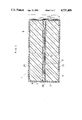
- FIGS. 1, 2, and 3 are cross-sectional views of different embodiments of the present invention.
- FIG. 4 is a diagrammatic view of a plasma polymerization apparatus.
- FIGS. 1, 2, and 3 Three different, preferred embodiments of the opto-magnetic recording medium of the present invention are illustrated in FIGS. 1, 2, and 3.
- the magneto-optical recording medium according to the present invention is generally designated at 1 as comprising a substrate 21 having a pair of opposed major surfaces and a magnetizable thin-film layer 5 on one substrate major surface.
- the medium further includes an undercoat layer 31 of plasma-polymerized film formed on the surface of the magnetizable layer 5 adjacent to the substrate, and/or a protective layer 35 of plasma-polymerized film formed on the surface of the magnetizable layer 5 remote from the substrate.
- the substrates 21 for use in the magneto-optical recording medium according to the present invention are generally formed of resinous materials, typically acrylic resins, polycarbonate resins, epoxy resin, and olefinic resins such as polymethylpentene, but they may also be formed of glass, ceramic or similar materials.
- the substrates are of disk shape having a thickness of about 1.2 to 1.5 mm, but they may be formed in another shape, for example, tape and drum.
- the surface of such a disk-shaped substrate on which the magnetic thin-film layer is formed may be provided with a tracking groove.
- the groove has a depth of about ⁇ /8n, especially from ⁇ /7n to ⁇ /12n wherein ⁇ is the wave length of a laser beam used and n is the refractive index of the substrate.
- Those portions of the magnetic thin-film layer which are located on the bottom of the channels constitute recording tracks where writing and reading light beams are preferably directed from the rear surface of the substrate. With this construction, the reading S/N ratio is improved and a control signal of a greater magnitude is available for tracking.
- the undercoat layer 31 is preferably a plasma-polymerized thin film comprising carbon. It may consist essentially of carbon alone or carbon and at least one other element. When it is desired to form a plasma-polymerized film undercoat layer 31 containing carbon and another element, the other element may be selected from hydrogen (H), nitrogen (N), and oxygen (O), and mixtures thereof.
- Exemplary of the source gas from which the film is plasma polymerized are saturated and unsaturated hydrocarbons, for example, methane, ethane, propane, butane, pentane, ethylene, propylene, butene, butadiene, acetylene, methylacetylene, and the like, and mixtures thereof.
- they are gaseous at room temperature because of ease of operation.
- a hydrocarbon which is liquid at room temperature may be used as the source material for plasma polymerization.
- Another class of preferred source material include mixtures of at least one such hydrocarbon and at least one member selected from H 2 , O 2 , O 3 , H 2 O, N 2 , NO x (such as NO and N 2 O, and NO 2 ), NH 3 , CO, CO 2 , etc.
- the source material may optionally contain a minor proportion of silicon (Si), boron (B), phosphorus (P), sulfur (S), etc.
- the plasma-polymerized film undercoat layer 31 may be formed solely from carbon by adding a large volume of hydrogen to a hydrocarbon gas, and subjecting the gas mixture to plasma polymerization to produce a carbon film.
- the resulting carbon film varies its carbon structure depending on mixed gas ratio, plasma exciting power, substrate temperature, and other parameters.
- the plasma-polymerized film undercoat layer 31 is generally formed to a thickness of about 10 to about 1,000 ⁇ . No additional advantage is obtained with undercoat layers in excess of 1,000 ⁇ and it is thus unnecessary to increase the thickness beyond this upper limit. Undercoat layers thinner than 10 ⁇ are ineffective. It is to be noted that the film thickness may be measured by means of an ellipsometer, for example.
- Control of film thickness in forming the plasma-polymerized film undercoat layer 31 may be done by controlling reaction time, source gas flow rate, and the like.
- the plasma-polymerized film is prepared by using the above-mentioned source gas, for example, hydrocarbon, creating an electrical discharge plasma of the gas, and contacting the plasma with the substrate.
- source gas for example, hydrocarbon
- gaseous molecules Since gaseous molecules have a less chance of collision with electrons and absorb little energy, they are kept at a tempeature approximate to room temperature.
- a low temperature plasma Such a system in which the kinetic energy (electron temperature) of electrons and the thermal motion (gas temperature) of molecules are not correlated is designated a low temperature plasma.
- chemical species set up the state capable of additive chemical reaction such as polymerization while being kept relatively unchanged from the original.
- Substrates are plasma treated under these conditions according to the present invention.
- the use of a low temperature plasma avoids any thermal influence on substrate.
- FIG. 4 illustrates a typical apparatus in which a substrate on its surface is treated with a plasma.
- This plasma apparatus uses a variable frequency power source.
- the apparatus comprises a reactor vessel R into which a source gas or gases are introduced from a source 511 and/or 512 through a mass flow controller 521 and/or 522.
- a source gas or gases are introduced from a source 511 and/or 512 through a mass flow controller 521 and/or 522.
- different gases from the sources 511 and 512 may be mixed in a mixer 53 to introduce a gas mixture into the reactor vessel.
- the source gases each may be fed at a flow rate of 1 to 250 ml per minute.
- a substrate to be treated 111 rests on a rotary electrode 552.
- Another electrode 551 is opposed to the rotary electrode 552 so as to sandwich the substrate 111 therebetween.
- One electrode 551 is connected to a variable frequency power source 54 and the other rotary electrode 552 grounded at 81.
- the reactor vessel R is further connected to a vacuum system for evacuating the vessel, including a vacuum pump in the form of an oil rotary pump 56, a liquefied nitrogen trap 57, an oil diffusion pump 58, and a vacuum controller 59.
- the vacuum system has the capacity of evacuating and keeping the reactor vessel R at a vacuum of 0.01 to 10 Torr.
- the reactor vessel R is first evacuated by means of the vacuum pump to a vacuum of 10 -5 Torr or lower before a source gas or gases are fed into the vessel at a given flow rate. Then the interior of the reactor vessel is maintained at a vacuum of 0.01 to 10 Torr.
- the variable frequency power 54 is turned on to generate a plasma with which a plasma-polymerized film is formed on the substrate.
- a carrier gas may be used, for example, Ar, N 2 , He, and H 2 .
- Operating parameters such as applied current and treating time may be as usual and properly chosen without undue experimentation.
- Plasma generation may be conducted by microwave discharge, DC discharge, and AC discharge as well as commmonly used high frequency discharge.
- the thus produced plasma-polymerized film undercoat layer 31 contains C and at least one optional element of H, N, and O as previously mentioned.
- the carbon content ranges from 30 to 100 atom% of the plasma-polymerized film undercoat layer, preferably from 30 to 90 atom%. Carbon contents of less than 30 atom% results in weak plasma-polymerized films which are impractical.
- H, N, and O contained along with C that the atomic ratio of hydrogen to carbon (H/C) is up to 1, especially from 1/6 to 1, the atomic ratio of nitrogen to carbon (N/C) is up to 3/10, especially from 1/20 to 3/10, and the atomic ratio of oxygen to carbon (O/C) is up to 3/10, especially from 1/20 to 3/10.
- H/C hydrogen to carbon
- N/C nitrogen to carbon
- O/C oxygen to carbon
- the contents of C, H, N, O and other elements in the plasma-polymerized film undercoat layer 31 may be determined by SIMS (secondary ion mass spectroscopy), for example.
- SIMS secondary ion mass spectroscopy
- the contents of C, H, N, O and other elements may be calculated by determining the count of the respective elements.
- the measurement of SIMS may be in accord with the article "SIMS and LAMMA" in the Surface Science Basic Lectures, Vol. 3, 1984 (Tokyo), Elementary and Application of Surface Analysis, page 70.
- the contents of C, H, N, O and other elements may be calculated by determining the profile of the respective elements while effecting ion etching with Ar or the like.
- the plasma-polymerized film undercoat layer 31 is preferably formed on the substrate 21 which has been plasma treated.
- the surface of the substrate become more adherent by treating with a plasma, and the adherence between the substrate and the undercoat layer is improved.
- the plasma treatment of the substrate surface may be effected by substantially the same process as previously described for the plasma polymerization with respect to its principle, operation, and conditions. The difference is that an inorganic gas is used as the treating gas in the plasma treatment of the substrate whereas the formation of plasma-polymerized film undercoat layer 31 by plasma polymerization uses an organic gas optionally containing an inorganic gas as the souce gas.
- the treating gas employed in the plasma treatment of the substrate is not particularly limited. Any inorganic gas may be used for the purpose, for example, H 2 , Ar, He, O 2 , N 2 , air, NH 3 , O 3 , H 2 O, NO x (such as NO, N 2 0, and NO 2 ), and mixtures thereof.
- the type of the electric source used for the plasma treatment is not particularly limited, and DC, AC, and microwave sources may be used.
- the plasma-polymerized film undercoat layer 31 is formed on the thus plasma-treated substrate 21.
- the magnetic thin-film layer 5 is formed on the plasma-polymerized film undercoat layer 31 with or without interposing an intermediate layer 4 therebetween.
- the magnetic thin-film layer 5 is a layer in which signals indicative of information are magnetically recorded using a modulated thermal beam or modulated magnetic field and the recorded signals are reproduced through magnetic-to-optical signal conversion. Most preferred for this purpose are so-called perpendicular magnetizable films.
- the magnetic thin-film layers are generally formed from alloys containing rare earth elements and transition metals by conventional techniques such as sputtering and vacuum deposition to produce an amorphous film to an ordinary thickness.
- the rare earth elements and transition metals used include all the members of their chemically defined classes.
- the preferred rare earth elements are gadolinium (Gd) and terbium (Tb), and the preferred transition metals are iron (Fe) and cobalt (Co). Their preferred combinations are GdFe, TbFe, TbFeCo, GdFeCo, GdTbFe, GdTbFeCo, etc.
- the rare earth metals and transition metals comprise 15 to 35 atom% and 65 to 85 atom% of the layer, respectively.
- the magnetic thin-film layers are preferably 0.05 to 0.1 ⁇ m thick.
- the magnetic thin-film layer 5 may be formed on the substrate through the intermediate layer 4 as previously mentioned.
- the intermediate layer 4 may be formed from such materials as SiO 2 , SiO, AlN, Si 3 N 4 , and ZnS by vacuum deposition or sputtering.
- the intermediate layer has a thickness of 0.05 to 0.2 ⁇ m.
- the protective layer 35 is formed from a plasma-polymerized film as previously mentioned.
- the protective layer 35 of plasma-polymerized film may be formed by substantially the same process as previously described for the plasma-polymerized film undercoat layer 31 with respect to its principle, operation, and conditions. This is also true for the composition and thickness of plasma-polymerized film.
- the plasma-polymerized film protective layer 35 is preferably formed so as to completely cover the magnetic thin-film layer 5 as shown in FIG. 3.
- the material of which the second protective layer 6 is made is not particularly limited.
- the second protective layers may be formed from either organic materials such as radiation-curable compounds, thermosetting resins, two-part reactive curing compositions, and thermoplastic resins or inorganic materials such as silicon oxide and silicon nitride. Most preferred among them are those obtained by curing radiation-curable compounds with radiation.
- Illustrative radiation-curable compounds include monomers, oligomers and polymers having contained or incorporated in their molecule groups capable of crosslinking or polymerizing upon exposure to radiation, for example, acrylic double bonds as given by acrylic and methacrylic acids having an unsaturated double bond capable of radical polymerization in response to an ionization energy and esters thereof, allyl double bonds as given by diallyl phthalate, and unsaturated bonds as given by maleic acid and maleic derivatives.
- the radiation-curable monomers used herein are those compounds having a molecular weight of less than 2,000 and the oligomers are those compounds having a molecular weight of 2,000 to 10,000.
- the radiation-curable compounds having unsaturated double bonds which may be used as oligomers and monomers in the present invention include styrene, ethylacrylate, ethylene glycol diacrylate, ethylene glycol dimethacrylate, diethylene glycol acrylate, diethylene glycol dimethacrylate, 1,6-hexaneglycol diacrylate, and 1,6-hexaneglycol dimethacrylate.
- the radiation-curable oligomers include polyfunctional oligo-ester acrylates as represented by the following general formula: ##STR3## wherein R 1 and R 2 are alkyl and n is an integer, and acryl-modified urethane elastomers, and derivatives thereof having such a functional group as COOH incorporated therein.
- thermoplastic resins which are prepared by modifying thermoplastic resins to be radiation sensitive.
- Illustrative radiation-curable resins are thermoplastic resins having contained or incorporated in their molecule, groups capable of crosslinking or polymerizing upon exposure to radiation, for example, acrylic double bonds as given by acrylic and methacrylic acids having an unsaturated double bond capable of radical polymerization and esters thereof, allyl double bonds as given by diallyl phthalate, and unsaturated bonds as given by maleic acid and maleic derivatives.
- resins which can be modified to be radiation curable include polyfunctional polyester resins, polyether ester resins, polyvinyl pyrrolidone resins and derivatives (e.g., PVP-olefin copolymers), polyamide resins, polyimide resins, phenol resins, spiroacetal resins, and acrylic resins comprising as a polymerization component at least one acryl or methacryl ester having a hydroxyl group.
- the second protective layer 6 has a thickness of about 0.1 to 30 ⁇ m, preferably about 1 to 10 ⁇ m. Films of less than 0.1 ⁇ m thick are difficult to produce as a uniform film, less moisture proof in a highly humid atmosphere, and thus insufficient to improve the durability of the magnetic thin-film layer 5. Films in excess of 30 ⁇ m thick are impractical because their shrinkage during curing causes the recording medium to be warped and cracks to occur in the protective layers.
- the protective layer may be formed by coating an appropriate composition by any well-known coating methods such as spinner coating, gravure coating, and spray coating.
- the conditions under which the film is coated may be suitably chosen by taking into account the viscosity of the polymer component in the composition, the substrate surface state, and the intended coating thickness.
- These radiation-curable resins may be cured by any of various well-known methods using electron or ultraviolet radiation.
- a photo polymerization sensitizer may be added to the radiation curable compounds as mentioned above.
- the photo polymerization sensitizers used herein may be selected from well-known sensitizers.
- Examples of such sensitizers include benzoins such as benzoin methyl ether, benzoin ethyl ether, ⁇ -methylbenzoin, ⁇ -chlorodeoxybenzoin, etc.; ketones such as benzophenone, acetophenone, bis(dialkylamino)benzophenones; quinones such as anthraquinone and phenanthraquinone; and sulfides such as benzyl sulfide, tetramethylthiuram monosulfide, etc.
- the photo polymerization sensitizers may be added in amounts of 0.1 to 10% by weight based on the resin solids.
- UV lamps such as xenon discharge lamps and hydrogen discharge lamps.
- Electron radiation may also be used.
- a radiation accelerator is operated at an accelerating voltage of 100 to 750 kV, more preferably 150 to 300 kV to generate radiation having a sufficient penetrating power such that the object is exposed to a radiation dose of 0.5 to 20 megarad.
- Particularly preferred types of radiation for exposure include radiation generated by a radiation accelerator and ultraviolet radiation because of ease of control of a dose, simple incorporation in a manufacturing line, and electromagnetic radiation shielding.
- the second protective layer 6 may be formed from inorganic materials. Included are thin films of oxides, for example, silicon monooxide, silicon dioxide, aluminum oxide, titanium oxide, and zinc oxide, and nitrides, for example, silicon nitride, aluminum nitride, titanium nitride, and boron nitride. These thin films have a thickness of about 0.1 to about 10 ⁇ m and are prepared by vacuum deposition or sputtering, for example.
- oxides for example, silicon monooxide, silicon dioxide, aluminum oxide, titanium oxide, and zinc oxide
- nitrides for example, silicon nitride, aluminum nitride, titanium nitride, and boron nitride.
- another substrate 25 may preferably be combined with the substrate 21 via a bonding layer 7 so as to sandwich the layers as previously formed on the substrate 21 between the substrates 21 and 25 as shown in FIG. 3.
- the second substrate 25 to be paired with the first substrate 21 has substantially the same shape as the first substrate 21, but may be made of any suitably chosen resinous material depending on the intended application of the medium.
- the second substrate 25 to be paired therewith is usually only required to serve as a protective plate. No strict requirements like transparency are thus imposed on the resinous material of the second substrate 25, and a variety of resins may be employed, for example, thermoplastic resins such as polyethylene, polyvinyl chloride, polystyrene, polypropylene, polyvinyl alcohol, methacrylic resins, polyamides, polyvinylidene chloride, polycarbonates, polyacetals, and fluorine resins; and thermosetting resins such as phenolic resins, urea resins, unsaturated polyester resins, polyurethanes, alkyd resins, melamine resins, epoxy resins, and silicone resins. Also employable to form the second substrate 25 are inorganic materials such as glass and ceramic materials.
- the bonding layer 7 may be an adhesive such as a hot-melt resin adhesive compound.
- a so-called both-side recording medium may be produced by forming on the inside surface of the second substrate 25, an additional set of necessary layers of plasma-polymerized film undercoat layer and magnetic thin-film layer so that the resulting assembly has two magnetic thin-film layers which can be recorded or read out from the side of the respective substrates 21 and 25.
- the second substrate 25 is generally formed from the same material as the first substrate 21 which is previously exemplified.
- the overall area of the outside surfaces of the above-mentioned medium namely the outside and inside peripheral surfaces and face and back surfaces of a disk-shaped medium, for example, is continuously covered with a coating layer 8 as shown in FIG. 3.
- the coating layer 8 is formed from a cured film of a radiation-curable compound.
- the particular radiation-curable compound used for this purpose may be selected from the compounds previously described in connection with the protective layer 6.
- the coating layer 8 in the form of a cured film of radiation-curable compound has a thickness of about 0.1 to 30 ⁇ m, preferably about 1 to 10 ⁇ m. Films of less than 0.1 ⁇ m thick are difficult to produce as a uniform film, less moisture proof in a highly humid atmosphere, and thus insufficient to improve the durability of the magnetic thin-film layer 5. Films in excess of 30 ⁇ m thick are impractical because their shrinkage during curing causes the recording medium to be warped and cracks to occur in the coating layer.
- the coating layer may be formed by coating an appropriate composition by any well-known coating methods such as spinner coating, gravure coating, and spray coating.
- the conditions under which the film is coated may be suitably chosen by taking into account the viscosity of the coating composition, the substrate surface state, and the intended coating thickness.
- the radiation-curable composition may be cured into a cured film or coating layer 8 by any of various well-known methods using electron or ultraviolet radiation as previously mentioned.
- the magneto-optical recording medium having a plasma-polymerized film undercoat layer between a substrate and a magnetic thin-film layer is moisture proof and durable in that the undercoat layer prevents deterioration of the magnetic layer due to entry of moisture from the substrate side.
- the magnetic thin-film layer is covered with the first protective layer of plasma-polymerized film and the second protective layer, moisture proofness is also imparted to the magnetic layer on the side remote from the substrate, leading to a durability improvement.
- the resulting medium is significantly improved in moisture proofness and durability and thus experiences minimized deterioration even after an extended shelf storage in a high temperature, high humidity environment.
- an intermediate layer 4 of Si 3 N 4 was formed to a thickness of 900 ⁇ by sputtering using a radio-frequency.
- a magnetic thin-film layer 5 was formed on the intermediate layer by sputtering to produce a TbFeCo alloy thin film of 0.1 ⁇ m thick.
- the target used in the sputtering was an Fe target having Tb and Co chips rested thereon.
- the magnetic layer-bearing substrate was placed in a vacuum chamber which was evacuated to a vacuum of 10 -5 Torr.
- a plasma-polymerized film 35 was formed on the magnetic thin-film layer 5 under the following conditions.
- the plasma-polymerized film is abbreviated as PPF in the following Tables and identified as type 1, 2, or 3 as defined above.
- Elemental analysis of these plasma-polymerized films was by SIMS and the film thickness was measured by means of an ellipsometer.
- a protecting layer 6 as formulated below was formed on the plasma-polymerized film 35.
- a coating composition of 100 parts by weight of a polyfunctional oligo-ester acrylate (trade name, Aronix M-8030) and 5 parts by weight of a photo-sensitizer (trade name, Bicure 55) was spinner coated on the plasma-polymerized film and exposed to ultraviolet radiation at 120 W/cm for 15 seconds for crosslinking and curing.
- the resulting protective layer had a thickness of 10 ⁇ m.
- C/N carrier to noise ratio
- a sample was measured for bit error rate of an EFM signal both at the initial and after storage in a 60° C., RH 90% atmosphere for 300 hours.
- the same substrate 21 as used in Example 1 was plasma treated under the following conditions before the plasma-polymerized film undercoat layer 31 was formed thereon under the same conditions as described in Example 1.
- the plasma treatment was effected by placing the substrate in a vacuum chamber which was evacuated to a vacuum of 10 -5 Torr. Argon was passed as the treating gas at a flow rate of 50 ml/min. under a gas pressure of 0.1 Torr while a high frequency voltage at 13.56 MHz was applied.
- the intermediate layer 4, magnetic thin-film layer 5, plasma-polymerized film protective layer 35, and second protective layer 6 were consecutively applied in the same manner as in Example 1, obtaining a series of magneto-optical recording media as shown in Table 2.
- the samples were measured for (1) C/N and (2) bit error rate as previously described in Example 1 and for (3) bond strength as will be defined below.
- An adhesive tape was applied to the magnetic layer side of the prepared magneto-optical recording medium sample under a certain pressure. The tape was then peeled off in a direction having an angle of 180° to the initial plane at a fixed rate to determine the force required in peeling.
- samples in which the substrate had not been subjected to a plasma treatment those samples having a plasma-polymerized film of a specific composition formed in place as exemplified by sample Nos. 204 and 205 exhibit properties which are slightly poorer than the plasma-treated substrate samples, but satisfactorily acceptable in actual applications.
- the same substrate 21 as used in Example 1 was plasma treated under the same conditions as used in Example 2 before the plasma-polymerized film undercoat layer 31 was formed thereon under the same conditions as described in Example 1.
- a second substrate 25 of PMMA having a diameter of 20 cm was bonded onto the second protective layer 6 using a hot melt resin adhesive.
- the resulting assembly was covered with a radiation-curable compound-containing coating composition of the following formulation by spinner coating or dipping whereupon the overall outside area of the paired substrates is covered with the coating.
- the coating was irradiated with UV radiation at 80 W/cm for 15 seconds for crosslinking and curing, obtaining a cured film having a thickness of 10 ⁇ m.
- C/N carrier to noise ratio
- the media based on the preferred constructure as illustrated in Example 2 and having another substrate as a protective plate and a coating layer of a specific composition covering the overall outside surfaces of the medium exhibit good shelf stability in severer conditions (60° C., RH 90%, 500 hr.)
Abstract
Description
__________________________________________________________________________
          Plasma-polymerized film
          1         2         3
__________________________________________________________________________
Source gas
          CH.sub.4 --100 SCCM
                    CH.sub.4 --50 SCCM
                              C.sub.2 H.sub.2 --75 SCCM
                    NH.sub.3 --50 SCCM
                              NO.sub.2 --25 SCCM
Carrier gas
          Ar--50 SCCM
                    Ar--50 SCCM
                              Ar--50 SCCM
Plasma generation
Pressure  0.1 Torr  0.1 Torr  0.1 Torr
Power     200 watts 200 watts 200 watts
Frequency 13.56 MHz 13.56 MHz 13.56 MHz
Film
Thickness 300Å  200Å  350Å
Composition
          H/C = 0.5 H/C = 0.3 H/C = 0.4
                    N/C = 0.08
                              N/C = 0.1
                              O/C = 0.15
__________________________________________________________________________
______________________________________
Rotating speed:    4      m/sec.
Carrier frequency: 500    kHz
Resolution:        30     kHz
Recording power:   3-4    mW at 830 nm
Reproducing power: 1      mW at 830 nm
______________________________________
              TABLE 1
______________________________________
     PPF
     pro-    Second
Sam- tective pro-
ple  layer,  tective C/N       Bit error rate (× 10.sup.-5)
No.  type    layer   Initial
                           ΔC/N
                                 Initial
                                        After storage
______________________________________
101  1       yes     51.6  -0.7  1.4    3.7
102  2       yes     51.8  -0.7  1.8    3.9
103  3       yes     52.1  -1.3  1.5    3.2
 104*
     --      yes     51.9  -1.4  1.7    5.3
 105*
     --      no      51.9  UM    1.6    Over scale
 106*
     1       no      51.7  -3.4  1.3    5.8
______________________________________
 *comparative samples
 UM = recording/reproducing operation unabled within 40 hours because
 numerous pinholes occurred.
(W/W0-1)×100%
                                  TABLE 2
__________________________________________________________________________
                                         Bit error rate
         PPF   PPF   Second         Bond (× 10.sup.-6)
Sample
    Plasma
         Undercoat,
               Protective
                     protective
                           C/N      strength After
No. treatment
         type, layer, type
                     layer Initial
                               ΔC/N
                                    increase
                                         Initial
                                             storage
__________________________________________________________________________
201 yes  1     1     yes   54.3
                               -0.4 55%  7.0 13.2
202 yes  2     2     yes   54.0
                               -0.4 50%  8.5 15.1
203 yes  3     3     yes   53.8
                               -0.6 60%  6.7 12.6
204 no   1     1     no    52.3
                               -3.3 25%  15.3
                                             70
205 no   1     1     yes   52.7
                               -0.7 30%  16.2
                                             31
206 yes  1     1     no    53.5
                               -3.6 50%  8.0 45
 207*
    no   1     --    no    52.5
                               UM after
                                    20%  14.4
                                             over
                               60 hr.        scale
 208*
    no   --    1     no    51.8
                               UM after
                                     0%  25.8
                                             over
                               60 hr.        scale
 209*
    no   --    --    no    51.5
                               UM after
                                     0%  27.2
                                             over
                               40 hr.        scale
__________________________________________________________________________
 *comparative samples
 UM = unmeasurable
______________________________________
Coating Composition
                   Parts by weight
______________________________________
Polyfunctional oligo-ester
                   100
acrylate (Aronix M-8030)
Photo-sensitizer (Bicure 55)
                    5
______________________________________
______________________________________
Rotating speed:    4      m/sec.
Carrier frequency: 500    kHz
Resolution:        30     kHz
Recording power:   3-4    mW at 830 nm
Reproducing power: 1      mW at 830 nm
______________________________________
              TABLE 3
______________________________________
      PPF        PPF
Sample
      Undercoat, Protective        C/N (dB)
No.   type       layer, type
                           Coating Initial
                                         ΔC/N
______________________________________
301   1          1         yes     54.6  -0.3
302   2          2         yes     53.9  -0.3
303   3          3         yes     53.6  -0.5
 304* 1          1         no      54.3  -3.0
 305* --         --        yes     51.8  -6.7
 306* --         --        no      51.5  UM
______________________________________
 *comparative samples
 UM = recording/reproducing operation unabled within 40 hours because
 numerous pinholes occurred.
Claims (32)
Applications Claiming Priority (6)
| Application Number | Priority Date | Filing Date | Title |
|---|---|---|---|
| JP60183285A JPS6243850A (en) | 1985-08-21 | 1985-08-21 | Photomagnetic recording medium |
| JP60-183285 | 1985-08-21 | ||
| JP60-184799 | 1985-08-22 | ||
| JP18479985A JPS6246447A (en) | 1985-08-22 | 1985-08-22 | Photomagnetic recording medium |
| JP60-185090 | 1985-08-23 | ||
| JP18509085A JPS6246448A (en) | 1985-08-23 | 1985-08-23 | Photomagnetic recording medium |
Publications (1)
| Publication Number | Publication Date |
|---|---|
| US4737408A true US4737408A (en) | 1988-04-12 |
Family
ID=27325282
Family Applications (1)
| Application Number | Title | Priority Date | Filing Date |
|---|---|---|---|
| US06/897,087 Expired - Lifetime US4737408A (en) | 1985-08-21 | 1986-08-18 | Magneto-optical recording medium having plasma-polymerized protective layers |
Country Status (1)
| Country | Link |
|---|---|
| US (1) | US4737408A (en) |
Cited By (20)
| Publication number | Priority date | Publication date | Assignee | Title |
|---|---|---|---|---|
| DE3836838A1 (en) * | 1987-10-30 | 1989-05-11 | Pioneer Electronic Corp | PHOTOMAGNETIC RECORDING MEDIUM WITH NON-SAEULUS FORMULA STRUCTURE |
| US4892634A (en) * | 1988-10-03 | 1990-01-09 | Eastman Kodak Company | Method of preparing thermo-magneto-optic recording elements |
| US4942073A (en) * | 1988-03-09 | 1990-07-17 | Hitachi, Ltd. | Optical data storage medium |
| EP0308981A3 (en) * | 1987-09-25 | 1990-08-08 | Hitachi Maxell Ltd. | An optical information recording medium and its production |
| US5053288A (en) * | 1987-11-20 | 1991-10-01 | Teijin Limited | Optical recording medium |
| US5143797A (en) * | 1988-08-30 | 1992-09-01 | Mitsubishi Denki Kabushiki Kaisha | Magneto-optic recording medium |
| US5311500A (en) * | 1988-01-22 | 1994-05-10 | Fuji Photo Film Co., Ltd. | Magneto-optical disk |
| WO1994029856A1 (en) * | 1993-06-11 | 1994-12-22 | Kabushiki Kaisha Toshiba | Optical recording medium and recording system |
| US5540988A (en) * | 1992-05-19 | 1996-07-30 | Canon Kabushiki Kaisha | Magneto-optical recording medium and process for producing the same |
| US5604005A (en) * | 1993-10-19 | 1997-02-18 | Tdk Corporation | Magneto-optical disc |
| US5667862A (en) * | 1989-03-15 | 1997-09-16 | Sony Corporation | Magneto-optical disk |
| US6083628A (en) * | 1994-11-04 | 2000-07-04 | Sigma Laboratories Of Arizona, Inc. | Hybrid polymer film |
| US6268073B1 (en) | 1998-11-09 | 2001-07-31 | Seagate Technology Llc | Flash layer overcoat for magnetically-induced super resolution magneto-optical media |
| US6324131B1 (en) | 1999-01-04 | 2001-11-27 | Seagate Technology Llc | Low glide magneto-optical recording medium |
| US6355342B1 (en) * | 1998-11-18 | 2002-03-12 | Seagate Technology Llc | Flash layer overcoat for high density multilayer magneto-optical media |
| US6381200B1 (en) | 1998-11-18 | 2002-04-30 | Seagate Technology Llc | Flash layer overcoat for first surface magneto-optical media |
| US20030218966A1 (en) * | 2001-02-21 | 2003-11-27 | Kuchman Todd J. | Optical disc and method of protecting same |
| US20040247891A1 (en) * | 2003-05-21 | 2004-12-09 | Samsung Electronics Co., Ltd. | Multi-layer structure and method of drawing microscopic structure therein, optical disc master and method of fabricating the same using the multi-layer structure, and optical disc manufactured using the optical disc master |
| US7212489B2 (en) | 2001-02-21 | 2007-05-01 | Scratch-Less Disc Industries, Llc | Optical disc and method of protecting same |
| US20070248784A1 (en) * | 2006-04-14 | 2007-10-25 | Seiji Morita | Recordable information recording medium and disk apparatus |
Citations (7)
| Publication number | Priority date | Publication date | Assignee | Title |
|---|---|---|---|---|
| JPS56109784A (en) * | 1980-02-06 | 1981-08-31 | Nippon Telegr & Teleph Corp <Ntt> | Laser-beam recording material |
| JPS5990246A (en) * | 1982-11-15 | 1984-05-24 | Nippon Telegr & Teleph Corp <Ntt> | Laser recording medium |
| JPS60180729A (en) * | 1984-02-28 | 1985-09-14 | Mitsubishi Electric Corp | Discharge machining device |
| JPS60181327A (en) * | 1984-02-22 | 1985-09-17 | Toray Ind Inc | Device for fasciated spinning |
| JPS60182767A (en) * | 1984-02-29 | 1985-09-18 | Nec Corp | Solid-state color image sensor |
| US4546464A (en) * | 1982-02-05 | 1985-10-08 | Matsushita Electric Industrial Co., Ltd. | Method of manufacturing an optical recording/reproducing disc |
| GB2164269A (en) * | 1984-08-18 | 1986-03-19 | Canon Kk | Magnetic recording medium |
-
1986
- 1986-08-18 US US06/897,087 patent/US4737408A/en not_active Expired - Lifetime
Patent Citations (7)
| Publication number | Priority date | Publication date | Assignee | Title |
|---|---|---|---|---|
| JPS56109784A (en) * | 1980-02-06 | 1981-08-31 | Nippon Telegr & Teleph Corp <Ntt> | Laser-beam recording material |
| US4546464A (en) * | 1982-02-05 | 1985-10-08 | Matsushita Electric Industrial Co., Ltd. | Method of manufacturing an optical recording/reproducing disc |
| JPS5990246A (en) * | 1982-11-15 | 1984-05-24 | Nippon Telegr & Teleph Corp <Ntt> | Laser recording medium |
| JPS60181327A (en) * | 1984-02-22 | 1985-09-17 | Toray Ind Inc | Device for fasciated spinning |
| JPS60180729A (en) * | 1984-02-28 | 1985-09-14 | Mitsubishi Electric Corp | Discharge machining device |
| JPS60182767A (en) * | 1984-02-29 | 1985-09-18 | Nec Corp | Solid-state color image sensor |
| GB2164269A (en) * | 1984-08-18 | 1986-03-19 | Canon Kk | Magnetic recording medium |
Cited By (29)
| Publication number | Priority date | Publication date | Assignee | Title |
|---|---|---|---|---|
| EP0308981A3 (en) * | 1987-09-25 | 1990-08-08 | Hitachi Maxell Ltd. | An optical information recording medium and its production |
| DE3836838A1 (en) * | 1987-10-30 | 1989-05-11 | Pioneer Electronic Corp | PHOTOMAGNETIC RECORDING MEDIUM WITH NON-SAEULUS FORMULA STRUCTURE |
| US5135819A (en) * | 1987-10-30 | 1992-08-04 | Pioneer Electronic Corporation | Photomagnetic memory medium having a non-columnar structure |
| US5053288A (en) * | 1987-11-20 | 1991-10-01 | Teijin Limited | Optical recording medium |
| US5311500A (en) * | 1988-01-22 | 1994-05-10 | Fuji Photo Film Co., Ltd. | Magneto-optical disk |
| US4942073A (en) * | 1988-03-09 | 1990-07-17 | Hitachi, Ltd. | Optical data storage medium |
| US5143797A (en) * | 1988-08-30 | 1992-09-01 | Mitsubishi Denki Kabushiki Kaisha | Magneto-optic recording medium |
| US4892634A (en) * | 1988-10-03 | 1990-01-09 | Eastman Kodak Company | Method of preparing thermo-magneto-optic recording elements |
| US5667862A (en) * | 1989-03-15 | 1997-09-16 | Sony Corporation | Magneto-optical disk |
| US5540988A (en) * | 1992-05-19 | 1996-07-30 | Canon Kabushiki Kaisha | Magneto-optical recording medium and process for producing the same |
| WO1994029856A1 (en) * | 1993-06-11 | 1994-12-22 | Kabushiki Kaisha Toshiba | Optical recording medium and recording system |
| US5796708A (en) * | 1993-06-11 | 1998-08-18 | Kabushiki Kaisha Toshiba | Optical recording medium and recording system |
| US5604005A (en) * | 1993-10-19 | 1997-02-18 | Tdk Corporation | Magneto-optical disc |
| US6083628A (en) * | 1994-11-04 | 2000-07-04 | Sigma Laboratories Of Arizona, Inc. | Hybrid polymer film |
| US6268073B1 (en) | 1998-11-09 | 2001-07-31 | Seagate Technology Llc | Flash layer overcoat for magnetically-induced super resolution magneto-optical media |
| US6355342B1 (en) * | 1998-11-18 | 2002-03-12 | Seagate Technology Llc | Flash layer overcoat for high density multilayer magneto-optical media |
| US6381200B1 (en) | 1998-11-18 | 2002-04-30 | Seagate Technology Llc | Flash layer overcoat for first surface magneto-optical media |
| US6324131B1 (en) | 1999-01-04 | 2001-11-27 | Seagate Technology Llc | Low glide magneto-optical recording medium |
| US20050094543A1 (en) * | 2001-02-21 | 2005-05-05 | Kuchman Todd J. | Optical disc and method of protecting same |
| US6842409B2 (en) | 2001-02-21 | 2005-01-11 | Scratch-Less Disc Industries, Llc | Optical disc and method of protecting same |
| US20030218966A1 (en) * | 2001-02-21 | 2003-11-27 | Kuchman Todd J. | Optical disc and method of protecting same |
| US20050243704A1 (en) * | 2001-02-21 | 2005-11-03 | Kuchman Todd J | Optical disc and method of protecting same |
| US7102985B2 (en) | 2001-02-21 | 2006-09-05 | Scratch-Less Disc Industries, Llc | Optical disc and method of protecting same |
| US7212489B2 (en) | 2001-02-21 | 2007-05-01 | Scratch-Less Disc Industries, Llc | Optical disc and method of protecting same |
| US20070237063A1 (en) * | 2001-02-21 | 2007-10-11 | Scratch-Less Disc Industries, Llc | Optical disc and method of protecting same |
| US7417941B2 (en) | 2001-02-21 | 2008-08-26 | Scratch-Less Disc Industries, Llc | Optical disc and method of protecting same |
| US20040247891A1 (en) * | 2003-05-21 | 2004-12-09 | Samsung Electronics Co., Ltd. | Multi-layer structure and method of drawing microscopic structure therein, optical disc master and method of fabricating the same using the multi-layer structure, and optical disc manufactured using the optical disc master |
| US7435468B2 (en) * | 2003-05-21 | 2008-10-14 | Samsung Electronics Co., Ltd. | Multi-layer structure and method of drawing microscopic structure therein, optical disc master and method of fabricating the same using the multi-layer structure, and optical disc manufactured using the optical disc master |
| US20070248784A1 (en) * | 2006-04-14 | 2007-10-25 | Seiji Morita | Recordable information recording medium and disk apparatus |
Similar Documents
| Publication | Publication Date | Title |
|---|---|---|
| US4737408A (en) | Magneto-optical recording medium having plasma-polymerized protective layers | |
| JPH0778915B2 (en) | Method for manufacturing magneto-optical recording medium | |
| JP2594422B2 (en) | Magneto-optical recording medium | |
| JP2543832B2 (en) | Magneto-optical recording medium | |
| JPS63166039A (en) | Optical recording medium | |
| JPS6246448A (en) | Photomagnetic recording medium | |
| JPS62281143A (en) | Magneto-optical recording medium | |
| JPS6246447A (en) | Photomagnetic recording medium | |
| JPS6240652A (en) | Photomagnetic recording medium | |
| US5571629A (en) | Optical recording medium | |
| JPS62281144A (en) | Magneto-optical recording medium | |
| JPS6292250A (en) | Information recording medium | |
| JPS6243850A (en) | Photomagnetic recording medium | |
| JPS6243849A (en) | Photomagnetic recording medium | |
| JP2523300B2 (en) | Optical recording medium | |
| JP2554482B2 (en) | Optical recording medium | |
| JP2711533B2 (en) | Optical recording medium | |
| JPS63251950A (en) | Optical recording medium | |
| JPS6240651A (en) | Photomagnetic recording medium | |
| JPS62281142A (en) | Magneto-optical recording medium | |
| JPS63166038A (en) | Optical recording medium | |
| JPS63200335A (en) | Optical recording medium | |
| JPS63197041A (en) | Optical recording medium and its production | |
| JPS62281141A (en) | Magneto-optical recording medium | |
| JP2554482C (en) |
Legal Events
| Date | Code | Title | Description |
|---|---|---|---|
| AS | Assignment |
Owner name: TDK CORPORATION, 13-1, NIHONBASHI 1-CHOME, CHUO-KU Free format text: ASSIGNMENT OF ASSIGNORS INTEREST.;ASSIGNORS:KUWAHARA, TSUNEO;NAKAYAMA, MASATOSHI;HIRATA, HIDEKI;REEL/FRAME:004842/0394 Effective date: 19860801 Owner name: TDK CORPORATION,JAPAN Free format text: ASSIGNMENT OF ASSIGNORS INTEREST;ASSIGNORS:KUWAHARA, TSUNEO;NAKAYAMA, MASATOSHI;HIRATA, HIDEKI;REEL/FRAME:004842/0394 Effective date: 19860801 |
|
| STCF | Information on status: patent grant |
Free format text: PATENTED CASE |
|
| CC | Certificate of correction | ||
| FEPP | Fee payment procedure |
Free format text: PAYOR NUMBER ASSIGNED (ORIGINAL EVENT CODE: ASPN); ENTITY STATUS OF PATENT OWNER: LARGE ENTITY |
|
| FPAY | Fee payment |
Year of fee payment: 4 |
|
| FPAY | Fee payment |
Year of fee payment: 8 |
|
| FEPP | Fee payment procedure |
Free format text: PAYOR NUMBER ASSIGNED (ORIGINAL EVENT CODE: ASPN); ENTITY STATUS OF PATENT OWNER: LARGE ENTITY Free format text: PAYER NUMBER DE-ASSIGNED (ORIGINAL EVENT CODE: RMPN); ENTITY STATUS OF PATENT OWNER: LARGE ENTITY |
|
| FPAY | Fee payment |
Year of fee payment: 12 |