US4725971A - Digital system simulation method and apparatus - Google Patents
Digital system simulation method and apparatus Download PDFInfo
- Publication number
- US4725971A US4725971A US06/576,446 US57644684A US4725971A US 4725971 A US4725971 A US 4725971A US 57644684 A US57644684 A US 57644684A US 4725971 A US4725971 A US 4725971A
- Authority
- US
- United States
- Prior art keywords
- outputs
- inputs
- circuit
- defining
- output
- Prior art date
- Legal status (The legal status is an assumption and is not a legal conclusion. Google has not performed a legal analysis and makes no representation as to the accuracy of the status listed.)
- Expired - Lifetime
Links
Images


Classifications
-
- G—PHYSICS
- G06—COMPUTING; CALCULATING OR COUNTING
- G06F—ELECTRIC DIGITAL DATA PROCESSING
- G06F30/00—Computer-aided design [CAD]
- G06F30/30—Circuit design
- G06F30/32—Circuit design at the digital level
- G06F30/33—Design verification, e.g. functional simulation or model checking
Definitions
- the invention relates generally to digital system testing equipment and methods, and in particular, to a digital system simulation apparatus and method for investigating, through simulation, the behavior of a digital system design prior to hardware construction.
- the Yorktown Simulation Engine is an outgrowth of logic simulators which were developed as early as the mid-fifties. During the mid-fifties and early sixties, gate level simulation which however did not include delays, was available. In the later sixties and early seventies, gate level simulation employing some limited timing became availabe but was of limited use because of the amount of detail required to provide the logic simulation. Then, in the mid- to to late seventies, a well-known and well-supported system known as TEGAS was developed for the high level simulation of VLSI logic. This logic could employ for example thousands of logic gates. Also, in the late seventies, better simulation tools began to be developed, primarily for in-house use.
- primary objects of the invention are improved simulation apparatus and methods, available at reasonable cost, for enabling more system flexibility, more user control over the simulation system, and for providing additional simulation capability with respect to signal input and output, monitoring, system debugging, and operator/machine interaction.
- the invention relates to an apparatus and method for simulating the behavior of a digital system.
- the digital system has a plurality of connected circuit elements.
- the apparatus features circuitry for defining inputs to the circuit elements and capable of having at least four signal levels. The levels include a "0" signal level, a "1" signal level, a high impedance “Z” signal level, and an unknown "X” signal level.
- Circuitry further defines outputs of the circuit elements based upon the input signals and capable of having at least the four signal levels.
- the output defining circuitry includes circuitry for providing a "0" or a "1" output signal level even though one or more of the input signal levels are at either a "Z" or an "X” signal level.
- the simulation apparatus further includes circuit elements which are standard building blocks and which have as inputs, a first input port, a second input port, and a carry-in port, and as outputs, at least a first output port and a carry-out port.
- the apparatus for simulating the behavior of a digital circuit having a plurality of connected circuit elements features each circuit element having a defined input/output causal relationship.
- Circuitry is provided for tracing the signal value of at least one of the circuit element inputs and outputs for at least a selected change of condition of a logical combination of the inputs and outputs.
- Further circuitry provides a message display capability for displaying messages describing the traced circuit element inputs and outputs at times when the selected condition defined by the logical combination is attained.
- the apparatus features circuitry for establishing functional relationships between at least some of the circuit element inputs and outputs.
- a table look-up element stores the functional relationships as a plurality of table entries, each entry having an address which is a function of the input signal levels to the selected circuit element.
- the table is characterized by plural output entries for at least one combination of the inputs which defines a specific table entry address. The table entry is addressed by those inputs.
- the invention relates both to the apparatus as described above and the method related thereto.
- the method features allowing a defined output of a circuit element to assume a "0" or a "1" output level even though one or more of the inputs defining the output thereof are "Z” or "X".
- the method features tracing signal values of at least one of the circuit element inputs and outputs for at least a selected change of condition of a logical combination of the circuit elements inputs and outputs, and for thereafter displaying messages describing each traced circuit element input and output at times when the selected condition is attained.
- the method features the steps of establishing functional relationships between at least some circuit element inputs and outputs and storing the functionally related inputs and outputs in a table look-up memory wherein the memory has plural output entries associated with at least one table input entry.
- the method further features the capability of automatically combining separately defined functional relationships in the table for a circuit element wherein outputs of the circuit element are defined by common inputs. This feature provides for more efficient and reliable operation according to the inventive method.
- FIG. 1 is a schematic representation of the simulation apparatus according to the invention.
- FIG. 2 is a diagrammatic representation of the transformation from circuit description to electrical signal representation of a digital system to be analyzed
- FIG. 3 is a flow chart illustrating generally a simulation control process
- FIGS. 4 and 5 represent the method steps for a first aspect of the invention
- FIGS. 6 and 7 represent the method steps for a second aspect of the invention.
- FIG. 8 represents the method steps for another aspect of the simulation apparatus and method
- FIGS. 9-13 represent the method steps for a fourth aspect of the simulation apparatus and method.
- FIGS. 14-18 represent the method steps for a preferred embodiment according to the invention.
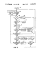
- a digital simulation system has a digital control circuitry 10 which connects to a keyboard 12, a monitor 14, and a printer 16.
- the digital simulation system will be described hereinafter in terms of a software controlled system although it could also be hardwired.
- the control circuitry 10 receives data information from the keyboard over, for example, a direct wire connection, a telephone line, or a small area or large area data communications network. In a similar manner, control circuitry 10 can supply display data to monitor 14.
- the printer 16 can be located either at the digital simulation control 10, or at another location, for example local to the keyboard and monitor, and can be connected to the control 10 through the same communication link as the keyboard and monitor.
- the illustrated embodiment of the invention is described and implemented primarily in software, illustrated in appendix A attached attached to U.S. Pat. No. 4,628,471 incorporated herein by reference, and the control apparatus 10 is a general purpose digital computer including a computer processing unit, RAM, and auxiliary memory.
- the control apparatus 10 is a general purpose digital computer including a computer processing unit, RAM, and auxiliary memory.
- any or all functions and components of the system can be constructed solely in hardware.
- a considerable loss of flexibility results, for example it is difficult to change a hardwired system; however on the other hand, the hardwired system will generally provide faster response time to the data inputs and a greater operating speed.
- the construction of a hardwired system in view of the disclosure hereinafter provided, is well within the skill of one practiced in the art.
- the general operation of the digital simulation control 10 is as follows. Referring to FIG. 2, the operator defines, through the keyboard, a circuit 17, the behavior of which to be simulated; and the control circuitry automatically provides an electrical signal data structure 18 describing the digital system. This occurs at what is generally called the command level of operation.
- the commands from the operator, through keyboard 12, to the digital simulation control 10 provide the digital simulation control with a unique definition of the interconnections of the digital circuit elements 19a, 19b, . . . , 19g making up the illustrated circuit 17.
- Those commands or instructions from the keyboard thus provide a complete description of how the circuit elements are connected.
- the circuit elements themselves are electrical elements with a set of "external pins" that define how the electrical elements can be connected to other elements of the circuit.
- the elements can be user defined or can be standard electrical building blocks, for example AND gates, OR gates, digital adders, etc.
- Each element of the circuit can have none, one, or several models associated therewith that define the alternatives for the element's functional performance when it is used during a logic simulation.
- An element can represent a real physical component, a portion of a real component, or a conceptual and hence generally non-physical component.
- An element is defined by its "component name" and can be referenced thereby.
- Input waveforms to the circuit are then specified by the operator, and commands from the keyboard 12 initiate simulation by the simulation control 10. This is indicated in FIG. 3 at 20.
- the apparatus employs an event timer, which is a unitless timer having a "time slot" for each unit of time as defined by the operator. During a time slot (or unit of time), a complete update of the digital circuitry input/output relationships will take place. The time slot can be on the order of nanoseconds or microseconds depending upon the nature of the digital system.
- the apparatus then maintains a list or schedule of the "events" or happenings during each time slot, and all of the events scheduled during a time slot are accounted for before the events scheduled for a next time slot can be considered.
- the events can be, for example, the changing of an output value, the monitoring of a value, the setting of a stop flag to indicate the processing of a "stop event", the propagation of a signal through a series of connected gates, etc.
- the apparatus begins a first clock cycle (or time slot) to determine whether there are any "events" scheduled to take place during this first time slot or cycle. This is indicated at 22. If no event is scheduled to take place during a time slot, the digital simulation control clock counter (referred to hereinafter as the event timer) increments, as indicated at 24, and the apparatus examines whether any "events" are to take place during the next time slot.
- the start command is given, as indicated at 20 of FIG. 3
- the apparatus begins a first clock cycle (or time slot) to determine whether there are any "events" scheduled to take place during this first time slot or cycle. This is indicated at 22. If no event is scheduled to take place during a time slot, the digital simulation control clock counter (referred to hereinafter as the event timer) increments, as indicated at 24, and the apparatus examines whether any "events" are to take place during the next time slot.
- the event timer increments, as indicated at 24, and the apparatus examines whether any "events" are to take place during
- the apparatus determines whether it is a "stop event” (at 26) in which case a stop flag is set at 28, or whether it is an "output event” (at 30).
- An output event requires the generation and update of output signal levels for the circuit element based upon input signal levels to the element. If an event is scheduled, but is neither an output event (indicated at 30) nor the stop event, an error condition is indicated at 32.
- Each output event causes particular circuit element output or outputs to be updated (at 34).
- a determination is then made (at 36) whether there are circuit elements downstream, that is, output receiving elements which are affected by the updated output. If there are affected elements downstream, their inputs are updated at 38 and thereafter those "fanout" elements are scheduled on the evaluation or simulation queue at 40. This means that at some later time (which can be within the same time slot), as specified in the definition for the particular circuit element, its output will be updated.
- the scheduling data is examined to determine if there are more events scheduled to occur during this "time slot" (indicated at 42). If more events are called for, the apparatus control returns to block 26 to begin determining the type of the next event. If there are no additional events, then the apparatus control determines whether the evaluation queue is empty for this time slot. This is indicated at 44. If it is not empty, the next element to be evaluated is obtained, at 46, and the element is evaluated at 48. The loop comprising element 44, 46, and 48 is repeatedly traversed until it is empty. Thereafter, the apparatus determines, at 50, whether there are more "events" occurring during this time slot. These events would have been generated and scheduled during the evaluation of the elements in the evaluation queue at 48. If addition events are scheduled for this time slot, control returns to the stop event determination at 26.
- the apparatus processes "last events".
- the "last events” are a special class of control events for which processing, for each time slot, occurs only after all other events in the time slot have been processed. "Last events” can include for example, evaluations relating to monitoring, tracing, sampling, breakpoints, etc.
- the apparatus control determines, at 54, whether the stop flag has been set, indicating that the stop event has been processed, and if the stop flag has not been set, the apparatus returns to the beginning of the processing method. In the event that the stop flag has been set, indicating the processing of a stop event, the apparatus returns to the "command level" parsers for further operation and the simulation stops, at least temporarily.
- the apparatus user has the capability of defining the input circuit elements through the keyboard 12.
- He can also use the system defined standard building blocks, such as adders, subtractors, AND or OR gates, etc.
- He has the capability of defining those circuit elements so that for a single particular combination of inputs, multiple outputs can be defined and further, so that an output can be defined as a "0", or a "1" even though an input to the circuit element is an undefined or high impedance signal level.
- the apparatus control 10 receives input data defining a circuit element from the user, through the keyboard 12, the apparatus generates and stores in memory, a "look-up table" which models the functional relationship between the inputs and outputs of the circuit element.
- a "look-up table” which models the functional relationship between the inputs and outputs of the circuit element.
- the user can define each output signal level separately base upon a logical or Boolean function of the value of the inputs (and outputs), or a specific functional relationship can be defined.
- the apparatus control 10 automatically combines in its data structure separately defined outputs which have a common set of inputs or allows the user to define for a common set of inputs, a plurality of outputs.
- the resulting "look-up table” takes the form of a stored data structure having a one-dimensional array of pointers to the new outputs values, the array being indexed by the current set of input (and output) signal values, hereinafter referred to as the "current state input vector" for the circuit element.
- Each data entry in the one-dimensional array list points to (and hence represents) the new output value(s) for the particular inputs forming the current state vector.
- the apparatus then "schedules" updating of the new output values.
- the element output value update indicated at 34 can be implemented as illustrated in FIGS. 4 and 5.
- the current state vector that is, the definition of element inputs and outputs which define the current input state to the circuit element, is formulated at 60 and is employed with the one-dimensional array defined during the circuit formulation stage of simulation to obtain a pointer to the new output values of various outputs of the circuit element. This is indicated at 62. Thereafter, the output signal values are updated, by first determining, at 64, if there is an output value to be updated and then scheduling each new output value change, at 66, until all of the output changes for this circuit element have been scheduled.
- the output values change at times schedulued in accordance with the definition of the circuit element which, through user supplied data, will generally take into account the delays inherent in signal transmission through physical media, internal device time delays, etc.
- the system continues to update other circuit elements, as noted at 36, for example those connected to those outputs of this circuit element, which change within this time period.
- the one-dimensional array of pointers is illustrated at 68.
- the array as noted above, is indexed by the input values to the circuit element; and the data stored therein points to the location in a memory of new values for the outputs as indicated at 70, 72, etc.
- the retrieved data also indicates the location of a next output, if any, whose output level is determined by this common set of input values.
- the content of the data stored at 70 points to the new output value data stored at 72.
- the present apparatus is capable of storing and using, in an efficient and reliable manner, multiple outputs related to a common set of inputs.
- a separate array and circuit element definition need not be set up for each output of a circuit element, where the signal level of the outputs are each functionally dependent upon a common set of inputs.
- the apparatus further provides, for a circuit element having undefined or high impedance inputs, the capability of defining the output signal level as a "0" or "1" level. It is well-known, that, for example for an adder, the input values can be a "0", a "1", an "X” which is an undefined input variable, or a "Z" which is a high impedance input. Typically, for an add circuit, an apparatus can employ truth tables similar to those of FIG. 6.
- the result of, for example, a two operand add with a carry-in bit has a defined "0" or "1" output level, such as at 76, even though one of the inputs to the adder is an "X" or a "Z".
- This method and apparatus thus allows the output of the adder to be "definite” even though the input is not and thereby provides a better correspondence to the actual operation of the digital system being simulated.
- FIG. 7 the evaluation of a function, such as an arithmetic function defined by the truth tables of FIG. 6, is described.
- This procedure corresponds to, for example, the evaluation indicated at 34 of FIG. 3.
- the type of circuit element being modeled is determined. This is indicated at 80.
- the procedure for modeling the function is initiated at 82 and execution of the procedure begins at 84.
- the procedure is implemented in a separately stored program which requires the computer program counter to be zeroed when the program is recalled and loaded into program member.
- Each "instruction" of the procedure or program as used herein represents one arithmetic step in evaluating the function.
- the step can be "add input A to input B".
- the type of instruction is determined at 88.
- the various instructions can be a control instruction, a status instruction, a relational instruction, an arithmetic instruction, and a logical instruction.
- the evaluation of the various nonarithmetic instruction types (at 89a, 89b, 89c, 89d) will be obvious, in accordance with the present invention, in view of the discussion which follows relating specifically to arithmetic instructions.
- the particular type of arithmetic instruction is then determined at 90. If the instruction is an ADD instruction, the operands are fetched and stored in operand registers and a "carry-in” bit is set to "0". This is indicated at 92. If a SUBTRACT instruction is called for, the operands are fetched and stored in the operand register at 94 and the complement of the second operand replaces the originally fetched operand. This is indicated at 96 (the complement of "X" or "Z” is "X"). The carry-in bit is set to "1". If a NEGATE instruction is called for, the operand is fetched and stored in one operand register at 98. The complement of the operand is then taken bit-by-bit and the carry-in bit is set to "0". This is indicated at 100. The second operand register is set to "1".
- the first bit of each operand, and the carry-in bit are fetched at 102 and the truth tables of FIG. 6 are employed (these are stored in the apparatus memory) to generate the resultant sum and a carry-out bit. This is indicated at 104.
- a sum bit register is then updated at 106 and the apparatus determines whether all of the bits in the operands have been used (at 108). If all of the bits have not been used, the next bit is fetched from the operand registers at 110 and the carry-out bit from the previous bit operation is employed as the new "carry-in" bit. This is indicated at 112.
- each element output signal is specified by a signal level which is calculated internally by the apparatus as being one of nine states. Three of those states have been previously described and designated as “0", “1", and "X”. The remaining states according to this illustrated embodiment of the invention, are a "weak 0", a “weak 1", a “weak X”, a “dynamic 0", a “dynamic 1”, and a “dynamic X” signal level.
- the apparatus herein is capable of operating both in a four signal-level mode and in a nine signal-level mode depending upon the requirements of the circuit element to which the signals are being provided. Consequently, for convenience, each signal level output is initially described using the nine signal-level mode. However, when a gate or function is receiving the output value, the nine values are reduced to four by masking the "strength" from the "change code” defining the output levels, and updating the new input values with the now four level signals.
- the update fanout element input 38 initially determines, at 110, the type of circuit element which is receiving the change at its input. If the circuit element is a transmission element, for example a MOS transistor operating like a switch, indicated at 112, or a bus gate (which is user transparent and is inserted automatically by the system) as indicated at 114, the input pins of the circuit elements are directly updated with the nine level output change, as indicated at 116. Thereafter, the circuit element is placed on the simulation queue for scheduling, as noted at 40 in FIGS. 3 and 8.
- a transmission element for example a MOS transistor operating like a switch, indicated at 112, or a bus gate (which is user transparent and is inserted automatically by the system) as indicated at 114
- the input pins of the circuit elements are directly updated with the nine level output change, as indicated at 116. Thereafter, the circuit element is placed on the simulation queue for scheduling, as noted at 40 in FIGS. 3 and 8.
- the receiving device is a simple gate or function, as indicated at 118, the signal level data or change code is processed by masking the strength data from the output.
- the new signal level change then consisting of only a four state signal, updates the pin value, at 120, and the device is then placed as noted above on the simulation queue is 40.
- the illustrated apparatus automatically, without user intervention, employs, as required, both the four level and nine level signals. Thereby, full capability of the system is maintained while reducing where possible the computational and memory requirements so that faster throughput is available.
- the strength information available to a gate or function, and which is irrelevant thereto is masked before the change value is made available to the element input.
- the apparatus provides the user with the capability of tracing signals and viewing the result of the trace procedure.
- tracing of the signal can be triggered on the change of value of a functional (for example Boolean) combination of pins, data paths, registers, memories, or memory windows.
- the operator provides the control 10 with the necessary information regarding the tracing procedure, including the functional expression, the satisfaction of which will trigger the trace message.
- the processing of the tracing command is initialized at the command level of the apparatus by parsing for example the Boolean expression of the events initiating a trace, into a stack, in Reverse Polish Notation (RPN). This is indicated at 130.
- the "RPN stack” is then processed to transform the parsed Boolean expressions into a network of event detectors, storage update watch blocks, and Boolean evaluators. This is indicated at 132.
- These elements become part of the defined circuit, the behavior of which is to be simulated, and are inserted into that circuit as would be any other circuit element. This is indicated at 134.
- the inclusion of these additional monitoring circuit elements is, however, transparent to the user, so that he is not aware of their inclusion into the circuit.
- the Boolean expression upon which a trace message is initiated is assumed to be [(A is positive) AND (B is negative)] OR (a change in memory location 1023).
- the apparatus traces upon either the detection of a circuit value A being positive when a circuit value B is negative, or a change in the value of the specific memory location.
- the detection of a positive A value and a negative B value is illustrated by a first and a second event detector 136, 138 respectively.
- a storage updated watch block 140 monitors the specified memory location.
- the event detector evaluation at 136, 138, and 140 is analogous to a simple gate evaluation.
- a one time-unit pulse is generated on the "output wire" which feeds a Boolean evaluator 142.
- the storage updated watch block receives the value of the memory location or locations to be monitored and intercepts storage updates of the selected registers. If an event is detected, the watch block 140 generates the one time-unit pulse and that pulse is received and detected by the Boolean evaluator 142.
- the Boolean evaluator detects the user specified Boolean combination of events and upon receiving the unit-time clock pulse triggers the generation of a trace message as described in more detail below if the Boolean combination is satisfied.
- the Boolean evaluator forms an index from the inputs available to it. This is indicated at 144.
- the resulting index is evaluated in accordance with a previously generated and stored evaluation table, at 146, and if the table result is true, at 148, at trace print message is generated at 150. If the table result is false, at 148, the trace print message is not generated.
- the event detectors 136 and 138 operate by forming an integer value based upon the inputs thereto, the integer value indicating the type of event. This is indicated at 144a. If the event is of a type which is increasing, as indicated at 146a, a check is made whether the new value is greater than the old value (at 148a) and if it is, an output of a unit-time pulse is generated at 150a. If the new value is not greater than the old value, at 148a, the unit-time pulse is not generated. In a similar manner, checks are made for an event type wherein the event is decreasing (at 152), where the event is changing (at 154), and where the event is not changing but is constant (156).
- the one unit time pulse is output. If the event is not properly detected, the one unit-time pulse is not output. The old value is then replaced by the new value of the monitored variable at 158. Similarly, if the negative output of blocks 146a, 152, 154, and 156 are all taken, an error condition is indicated at 160.
- the storage update watch block begins by checking whether the updated storage bits are the ones upon which a trace can be triggered. This is indicated at 162. If they are not, the control returns to other monitoring or evaluation processes. If the updated storage bits are being monitored, the apparatus determines whether it is a window trace at 164, in which case the output pulse is immediately generated at 166. Otherwise, the values being monitored are used to generate an integer value indicating the type of the event. Processing then follows using the same procedure as that described in connection with FIG. 12. Using the described process, tracing can be triggered by a functional combination of variables to monitor behavioral operation of the digital circuit 17. As in FIG. 12, if none of the tested events are found to exist, an error condition is indicated. Further, if the new value does not meet the required decision criteria relating to the old value, the unit pulse is not output.
- the apparatus provides the user with the further capability of interactively controlling sampling of waveforms not only at the time the circuitry is compiled (i.e. prior to actual simulation), but thereafter, during simulation itself.
- the user can interactively specify, during the actual simulation, which elements are to be automatically or continuously sampled and have their values recorded; when to turn the sampling on and off; and whether to sample at every occurrence of a specified condition or whether to periodically sample on the Nth occurrence of the specified condition, for example in response to breakpoints.
- the breakpoints, which can control sampling can also be set interactively during the simulation period).
- the user can also direct the apparatus to automatically and continuously print, or display for viewing, the values of specified circuit elements inputs and outputs.
- the user can temporarily stop the simulation, examine the desired stored values or printed files, and then return to the simulation, continuing where the simulation had left off.
- This advantageous procedure differs markedly from eearliestr simulation systems wherein the simulation, once interrupted, cannot thereafter be resumed as if the interruption had not occurred.
- the apparatus treats a command to begin or terminate sampling upon the occurrence of one or more specified conditions in the same manner in which it treats the command to trigger printing or recording of a trace message upon the occurrence of a specified function, for example based upon a combination of ANDed or ORed variables.
- FIG. 14 which corresponds to FIG.
- a Boolean expression which specifies when to initiate (or terminate) sampling, into a Reverse Polish Notation (RPN) stack, (at 190); transforming the RPN stack into a network of event detectors, storage update watch blocks, and Boolean evaluators (at 192); and inserting the resulting circuit elements into the network whose behavior is to be investigated (at 194).
- RPN Reverse Polish Notation
- Boolean evaluator corresponding to that of FIG. 14, detects an event upon which a sample command is to be generated, a sampling method, corresponding to the tracing procedure of FIGS. 11-13, is initiated.
- the apparatus When a command from the keyboard to create an apparatus structure for initiating and controlling sampling has been processed as illustrated in FIG. 14, the apparatus, after the network elements have been fully described, sets up a monitor data structure identifying the signal inputs and outputs to be monitored. Referring to FIG. 15, the apparatus creates a data structure in memory which consists of pointers to the values of all signals which are to be monitored. Thus, if there are signals to be monitored, as determined at 200, the nature of the signal is determined at 202, and a pointer is obtained which directs the apparatus to the memory storage location containing the value of that signal. This is indicated at 204. Thereafter, that pointer is stored in a monitor data structure of memory, at 206, for later use. When all of the signals to be monitored have been processed in this manner, the apparatus initializes (for example clears) a push-down stack, at 208, and returns control to the command level processing.
- the Boolean evaluator used for initating sampling forms an index based upon the inputs provided thereto. This is indicated at 230 and corresponds, as noted above, to the elements illustrated in FIG. 10.
- the result of the index is applied to an evaluation table (at 232), and if the evaluation table provides a "true" response to the index, at 234, the event (to perform a sample function) is detected. If the result at 234 is not true, control returns to the calling program. Once an event is detected, the determination is made whether that event has been detected previously in this time slot. This is indicated at 236. If the event has been detected, the Boolean evaluator circuitry returns control back to the main program.
- an event counter is incremented, at 238; and a flag is set, indicating that this event was detected during this specific time slot. This is indicated at 240. Thereby, the event and the time of the event are retained for later display and analysis.
- the event counter modulo the trigger modulus
- the sampling function is performed (at 244). If, in this time slot, a signal sample is not to be taken, the sample function at 244 is not performed. Then, a "last event" is scheduled for this time slot, to clear the event detected flag set previously at 240. This is indicated at 246.
- the sampling process which occurs during the simulation is illustrated in FIG. 17.
- the apparatus first determines, at 250, if there is a signal to be monitored, for example by examining the monitor data structure. If there is a signal to be monitored and sampled, the pointer to the signal value is obtained at 252 and the value itself is then obtained at 254. That value is placed (at 256) in the push-down stack previously initialized at 208. When all of the signals to be sampled have been thus processed, the command processing continues at 246 (FIG. 16).
- the results of the sampling process can viewed at the end of the simulation, however, it is desirable to provide the user with the capability of temporarily interrupting the simulation to view the sampled waveforms. Therefore, the apparatus and method provide a breakpoint capability for interrupting the simulation, viewing the sampled results, and thereafter resuming the simulation process where it had been interrupted.
- the breakpoints can be functionally related to a combination of signal values. The implementation and evaluation of the breakpoint corresponds to the implementation of the sampling and tracing procedures described in connection with FIGS. 9-18.
- the sampled values of the monitored signals can be printed by examining first the push-down stack, at 260, to determine whether there are any entries. If there are no entries, the print monitoring command processing ends. If there are entries, a determination is made whether they are list formatted in output (at 262) or waveform formatted in output (at 264). Depending upon the format used, the sampled values are displayed at 266 and 268, respectively. In the illustrated embodiment the only formats provided for displaying the output waveforms are the list and waveform formats. Any other output specification format in this illustrated embodiment would result in an error condition as indicated at 270.
- the resulting digital system simulation apparatus and method thus enable the user to advantageously and interactively control, during simulation, the tracing of signals in the digital system to be analyzed. Further, the behavior of the system can be approximated better by recognizing and allowing a precise definition of element outputs even though the element inputs can include undefined variables. Furthermore, the apparatus allows efficient and better utilization of system memory by having the capacity for defining multiple outputs of circuit elements where those outputs all have common inputs.
Abstract
Description
Claims (25)
Applications Claiming Priority (2)
| Application Number | Priority Date | Filing Date | Title |
|---|---|---|---|
| WO83/01741 | 1983-11-03 | ||
| PCT/US1983/001741 WO1985002033A1 (en) | 1983-11-03 | 1983-11-03 | Digital system simulation method and apparatus |
Publications (1)
| Publication Number | Publication Date |
|---|---|
| US4725971A true US4725971A (en) | 1988-02-16 |
Family
ID=22175557
Family Applications (2)
| Application Number | Title | Priority Date | Filing Date |
|---|---|---|---|
| US06/576,446 Expired - Lifetime US4725971A (en) | 1983-11-03 | 1984-02-02 | Digital system simulation method and apparatus |
| US06/576,364 Expired - Lifetime US4695968A (en) | 1983-11-03 | 1984-02-02 | Digital system simulation method and apparatus having improved sampling |
Family Applications After (1)
| Application Number | Title | Priority Date | Filing Date |
|---|---|---|---|
| US06/576,364 Expired - Lifetime US4695968A (en) | 1983-11-03 | 1984-02-02 | Digital system simulation method and apparatus having improved sampling |
Country Status (2)
| Country | Link |
|---|---|
| US (2) | US4725971A (en) |
| WO (1) | WO1985002033A1 (en) |
Cited By (40)
| Publication number | Priority date | Publication date | Assignee | Title |
|---|---|---|---|---|
| US4787061A (en) * | 1986-06-25 | 1988-11-22 | Ikos Systems, Inc. | Dual delay mode pipelined logic simulator |
| US4821173A (en) * | 1986-06-30 | 1989-04-11 | Motorola, Inc. | Wired "OR" bus evaluator for logic simulation |
| US4827427A (en) * | 1987-03-05 | 1989-05-02 | Hyduke Stanley M | Instantaneous incremental compiler for producing logic circuit designs |
| US4862347A (en) * | 1986-04-22 | 1989-08-29 | International Business Machine Corporation | System for simulating memory arrays in a logic simulation machine |
| US4866663A (en) * | 1987-02-13 | 1989-09-12 | Sanders Associates, Inc. | Simulation system |
| US4901259A (en) * | 1988-08-15 | 1990-02-13 | Lsi Logic Corporation | Asic emulator |
| US4907180A (en) * | 1987-05-04 | 1990-03-06 | Hewlett-Packard Company | Hardware switch level simulator for MOS circuits |
| US4937827A (en) * | 1985-03-01 | 1990-06-26 | Mentor Graphics Corporation | Circuit verification accessory |
| US4965758A (en) * | 1988-03-01 | 1990-10-23 | Digital Equipment Corporation | Aiding the design of an operation having timing interactions by operating a computer system |
| US5051941A (en) * | 1986-09-26 | 1991-09-24 | Hitachi, Ltd. | Method and apparatus for logical simulation |
| US5111413A (en) * | 1989-03-24 | 1992-05-05 | Vantage Analysis Systems, Inc. | Computer-aided engineering |
| US5155836A (en) * | 1987-01-27 | 1992-10-13 | Jordan Dale A | Block diagram system and method for controlling electronic instruments with simulated graphic display |
| US5157620A (en) * | 1988-05-31 | 1992-10-20 | International Computers Limited | Method for simulating a logic system |
| US5220662A (en) * | 1991-03-28 | 1993-06-15 | Bull Hn Information Systems Inc. | Logic equation fault analyzer |
| US5353289A (en) * | 1990-10-31 | 1994-10-04 | Nec Corporation | Fault judging device comprising a compression circuit for compressing output pattern signals of a circuit model |
| US5442772A (en) * | 1991-03-29 | 1995-08-15 | International Business Machines Corporation | Common breakpoint in virtual time logic simulation for parallel processors |
| US5530841A (en) * | 1990-12-21 | 1996-06-25 | Synopsys, Inc. | Method for converting a hardware independent user description of a logic circuit into hardware components |
| US5629858A (en) * | 1994-10-31 | 1997-05-13 | International Business Machines Corporation | CMOS transistor network to gate level model extractor for simulation, verification and test generation |
| US5633812A (en) * | 1992-09-29 | 1997-05-27 | International Business Machines Corporation | Fault simulation of testing for board circuit failures |
| US5680583A (en) * | 1994-02-16 | 1997-10-21 | Arkos Design, Inc. | Method and apparatus for a trace buffer in an emulation system |
| US5689683A (en) * | 1989-02-28 | 1997-11-18 | Nec Corporation | Hardware simulator capable of dealing with a description of a functional level |
| US5706476A (en) * | 1995-06-05 | 1998-01-06 | Synopsys, Inc. | Method and apparatus for use of the undefined logic state and mixed multiple-state abstractions in digital logic simulation |
| US5726918A (en) * | 1995-06-05 | 1998-03-10 | Synopsys, Inc. | Tool, system and method for dynamic timing analysis in a plural-instance digital system simulation |
| US5752000A (en) * | 1994-08-02 | 1998-05-12 | Cadence Design Systems, Inc. | System and method for simulating discrete functions using ordered decision arrays |
| US5784593A (en) * | 1995-09-29 | 1998-07-21 | Synopsys, Inc. | Simulator including process levelization |
| US5809283A (en) * | 1995-09-29 | 1998-09-15 | Synopsys, Inc. | Simulator for simulating systems including mixed triggers |
| US5819065A (en) * | 1995-06-28 | 1998-10-06 | Quickturn Design Systems, Inc. | System and method for emulating memory |
| US5822564A (en) * | 1996-06-03 | 1998-10-13 | Quickturn Design Systems, Inc. | Checkpointing in an emulation system |
| US5915124A (en) * | 1997-01-03 | 1999-06-22 | Ncr Corporation | Method and apparatus for a first device accessing computer memory and a second device detecting the access and responding by performing sequence of actions |
| US5920712A (en) * | 1994-05-13 | 1999-07-06 | Quickturn Design Systems, Inc. | Emulation system having multiple emulator clock cycles per emulated clock cycle |
| US5923865A (en) * | 1995-06-28 | 1999-07-13 | Quickturn Design Systems, Inc. | Emulation system having multiple emulated clock cycles per emulator clock cycle and improved signal routing |
| US5960191A (en) * | 1997-05-30 | 1999-09-28 | Quickturn Design Systems, Inc. | Emulation system with time-multiplexed interconnect |
| US5970240A (en) * | 1997-06-25 | 1999-10-19 | Quickturn Design Systems, Inc. | Method and apparatus for configurable memory emulation |
| US6053948A (en) * | 1995-06-07 | 2000-04-25 | Synopsys, Inc. | Method and apparatus using a memory model |
| US6285914B1 (en) | 1997-12-30 | 2001-09-04 | Hyundai Electronics Industries Co., Ltd. | Verification method by means of comparing internal state traces |
| US6377911B1 (en) * | 1988-12-02 | 2002-04-23 | Quickturn Design Systems, Inc. | Apparatus for emulation of electronic hardware system |
| US6510405B1 (en) * | 1998-12-22 | 2003-01-21 | Unisys Corporation | Method and apparatus for selectively displaying signal values generated by a logic simulator |
| US6604065B1 (en) | 1999-09-24 | 2003-08-05 | Intrinsity, Inc. | Multiple-state simulation for non-binary logic |
| US7031897B1 (en) | 1999-09-24 | 2006-04-18 | Intrinsity, Inc. | Software modeling of logic signals capable of holding more than two values |
| US7555424B2 (en) | 2006-03-16 | 2009-06-30 | Quickturn Design Systems, Inc. | Method and apparatus for rewinding emulated memory circuits |
Families Citing this family (15)
| Publication number | Priority date | Publication date | Assignee | Title |
|---|---|---|---|---|
| US4849880A (en) * | 1985-11-18 | 1989-07-18 | John Fluke Mfg. Co., Inc. | Virtual machine programming system |
| US4914568A (en) * | 1986-10-24 | 1990-04-03 | National Instruments, Inc. | Graphical system for modelling a process and associated method |
| US4901221A (en) * | 1986-04-14 | 1990-02-13 | National Instruments, Inc. | Graphical system for modelling a process and associated method |
| US4868770A (en) * | 1987-12-02 | 1989-09-19 | Analogy, Inc. | Simulation results enhancement method and system |
| US4916627A (en) * | 1987-12-02 | 1990-04-10 | International Business Machines Corporation | Logic path length reduction using boolean minimization |
| GB2234092A (en) * | 1989-05-12 | 1991-01-23 | Genrad Ltd | System for simulating operations of electronic circuit |
| US5369593A (en) * | 1989-05-31 | 1994-11-29 | Synopsys Inc. | System for and method of connecting a hardware modeling element to a hardware modeling system |
| US5353243A (en) * | 1989-05-31 | 1994-10-04 | Synopsys Inc. | Hardware modeling system and method of use |
| US5331571A (en) * | 1992-07-22 | 1994-07-19 | Nec Electronics, Inc. | Testing and emulation of integrated circuits |
| US5751592A (en) * | 1993-05-06 | 1998-05-12 | Matsushita Electric Industrial Co., Ltd. | Apparatus and method of supporting functional design of logic circuit and apparatus and method of verifying functional design of logic circuit |
| US6480817B1 (en) * | 1994-09-01 | 2002-11-12 | Hynix Semiconductor, Inc. | Integrated circuit I/O pad cell modeling |
| US5673295A (en) * | 1995-04-13 | 1997-09-30 | Synopsis, Incorporated | Method and apparatus for generating and synchronizing a plurality of digital signals |
| US5819072A (en) * | 1996-06-27 | 1998-10-06 | Unisys Corporation | Method of using a four-state simulator for testing integrated circuit designs having variable timing constraints |
| US5841967A (en) * | 1996-10-17 | 1998-11-24 | Quickturn Design Systems, Inc. | Method and apparatus for design verification using emulation and simulation |
| DE102008051401B4 (en) * | 2008-10-11 | 2010-08-05 | Festo Ag & Co. Kg | Training and simulation device for electrical functional processes in electrical, electromechanical and electro-fluidic systems |
Citations (11)
| Publication number | Priority date | Publication date | Assignee | Title |
|---|---|---|---|---|
| US3794981A (en) * | 1972-06-02 | 1974-02-26 | Singer Co | Realtime computer operation |
| US4064394A (en) * | 1975-05-28 | 1977-12-20 | American Chain & Cable Company, Inc. | Electronic digital process controller having simulated analog control functions |
| US4205370A (en) * | 1975-04-16 | 1980-05-27 | Honeywell Information Systems Inc. | Trace method and apparatus for use in a data processing system |
| US4306286A (en) * | 1979-06-29 | 1981-12-15 | International Business Machines Corporation | Logic simulation machine |
| US4308616A (en) * | 1979-05-29 | 1981-12-29 | Timoc Constantin C | Structure for physical fault simulation of digital logic |
| US4342093A (en) * | 1979-05-15 | 1982-07-27 | Hitachi, Ltd. | Method of digital logic simulation |
| US4494191A (en) * | 1981-06-25 | 1985-01-15 | Mitsubishi Denki Kabushiki Kaisha | Simulation unit sharing the same CPU as a programming control unit |
| US4527249A (en) * | 1982-10-22 | 1985-07-02 | Control Data Corporation | Simulator system for logic design validation |
| US4584642A (en) * | 1982-10-21 | 1986-04-22 | Tokyo Shibaura Denki Kabushiki Kaisha | Logic simulation apparatus |
| US4587625A (en) * | 1983-07-05 | 1986-05-06 | Motorola Inc. | Processor for simulating digital structures |
| US4628471A (en) * | 1984-02-02 | 1986-12-09 | Prime Computer, Inc. | Digital system simulation method and apparatus having two signal-level modes of operation |
Family Cites Families (4)
| Publication number | Priority date | Publication date | Assignee | Title |
|---|---|---|---|---|
| US4259077A (en) * | 1978-08-31 | 1981-03-31 | Keweza Joseph T | Wireless logic trainer |
| EP0047388A3 (en) * | 1980-09-05 | 1984-07-18 | Rockwell International Corporation | Computer aided design system |
| DD204788A1 (en) * | 1982-03-31 | 1983-12-07 | Gotthard Lasch | CIRCUIT ARRANGEMENT FOR IMPLEMENTING CIRCUITS IN A SYSTEM |
| US4656580A (en) * | 1982-06-11 | 1987-04-07 | International Business Machines Corporation | Logic simulation machine |
-
1983
- 1983-11-03 WO PCT/US1983/001741 patent/WO1985002033A1/en unknown
-
1984
- 1984-02-02 US US06/576,446 patent/US4725971A/en not_active Expired - Lifetime
- 1984-02-02 US US06/576,364 patent/US4695968A/en not_active Expired - Lifetime
Patent Citations (11)
| Publication number | Priority date | Publication date | Assignee | Title |
|---|---|---|---|---|
| US3794981A (en) * | 1972-06-02 | 1974-02-26 | Singer Co | Realtime computer operation |
| US4205370A (en) * | 1975-04-16 | 1980-05-27 | Honeywell Information Systems Inc. | Trace method and apparatus for use in a data processing system |
| US4064394A (en) * | 1975-05-28 | 1977-12-20 | American Chain & Cable Company, Inc. | Electronic digital process controller having simulated analog control functions |
| US4342093A (en) * | 1979-05-15 | 1982-07-27 | Hitachi, Ltd. | Method of digital logic simulation |
| US4308616A (en) * | 1979-05-29 | 1981-12-29 | Timoc Constantin C | Structure for physical fault simulation of digital logic |
| US4306286A (en) * | 1979-06-29 | 1981-12-15 | International Business Machines Corporation | Logic simulation machine |
| US4494191A (en) * | 1981-06-25 | 1985-01-15 | Mitsubishi Denki Kabushiki Kaisha | Simulation unit sharing the same CPU as a programming control unit |
| US4584642A (en) * | 1982-10-21 | 1986-04-22 | Tokyo Shibaura Denki Kabushiki Kaisha | Logic simulation apparatus |
| US4527249A (en) * | 1982-10-22 | 1985-07-02 | Control Data Corporation | Simulator system for logic design validation |
| US4587625A (en) * | 1983-07-05 | 1986-05-06 | Motorola Inc. | Processor for simulating digital structures |
| US4628471A (en) * | 1984-02-02 | 1986-12-09 | Prime Computer, Inc. | Digital system simulation method and apparatus having two signal-level modes of operation |
Non-Patent Citations (12)
| Title |
|---|
| 1978 IEEE International Symposium on Circuits and Systems Proceedings , 17th 19th May 1979, New York, pp. 5 10, IEEE, New York, G. R. Case, The Salogs Digital Logic Simulator . * |
| 1978 IEEE International Symposium on Circuits and Systems Proceedings, 17th-19th May 1979, New York, pp. 5-10, IEEE, New York, G. R. Case, "The Salogs Digital Logic Simulator". |
| Denneau, "The Yorktown Simulation Engine", 19th Design Automation Conference, 1982 IEEE, paper 7.2, pp. 55-59. |
| Denneau, The Yorktown Simulation Engine , 19th Design Automation Conference, 1982 IEEE, paper 7.2, pp. 55 59. * |
| IBM Technical Disclosure Bulletin, vol. 25, No. 1, Jun. 1982, pp. 138 145, New York, G. S. Miranker, Logical, Device Level Simulation of MOS Networks . * |
| IBM Technical Disclosure Bulletin, vol. 25, No. 1, Jun. 1982, pp. 138-145, New York, G. S. Miranker, "Logical, Device Level Simulation of MOS Networks". |
| Krontstadt et al, "Software Support for the Yorktown Simulation Engine", 19th Design Automation Conference, 1982 IEEE, paper 7.3, pp. 60-64. |
| Krontstadt et al, Software Support for the Yorktown Simulation Engine , 19th Design Automation Conference, 1982 IEEE, paper 7.3, pp. 60 64. * |
| Mano, M., Digital Logic and Computer Design , pp. 72 87, 1979. * |
| Mano, M., Digital Logic and Computer Design, pp. 72-87, 1979. |
| Pfister, "Yorktown Simulation Engine: Introduction", 19th Design Automation Conference, 1982 IEEE, paper 7.1, pp. 51-54. |
| Pfister, Yorktown Simulation Engine: Introduction , 19th Design Automation Conference, 1982 IEEE, paper 7.1, pp. 51 54. * |
Cited By (47)
| Publication number | Priority date | Publication date | Assignee | Title |
|---|---|---|---|---|
| US4937827A (en) * | 1985-03-01 | 1990-06-26 | Mentor Graphics Corporation | Circuit verification accessory |
| US4862347A (en) * | 1986-04-22 | 1989-08-29 | International Business Machine Corporation | System for simulating memory arrays in a logic simulation machine |
| US4787061A (en) * | 1986-06-25 | 1988-11-22 | Ikos Systems, Inc. | Dual delay mode pipelined logic simulator |
| US4821173A (en) * | 1986-06-30 | 1989-04-11 | Motorola, Inc. | Wired "OR" bus evaluator for logic simulation |
| US5051941A (en) * | 1986-09-26 | 1991-09-24 | Hitachi, Ltd. | Method and apparatus for logical simulation |
| US5155836A (en) * | 1987-01-27 | 1992-10-13 | Jordan Dale A | Block diagram system and method for controlling electronic instruments with simulated graphic display |
| US4866663A (en) * | 1987-02-13 | 1989-09-12 | Sanders Associates, Inc. | Simulation system |
| US4827427A (en) * | 1987-03-05 | 1989-05-02 | Hyduke Stanley M | Instantaneous incremental compiler for producing logic circuit designs |
| US4907180A (en) * | 1987-05-04 | 1990-03-06 | Hewlett-Packard Company | Hardware switch level simulator for MOS circuits |
| US4965758A (en) * | 1988-03-01 | 1990-10-23 | Digital Equipment Corporation | Aiding the design of an operation having timing interactions by operating a computer system |
| US5157620A (en) * | 1988-05-31 | 1992-10-20 | International Computers Limited | Method for simulating a logic system |
| US4901259A (en) * | 1988-08-15 | 1990-02-13 | Lsi Logic Corporation | Asic emulator |
| US6842729B2 (en) | 1988-12-02 | 2005-01-11 | Quickturn Design Systems, Inc. | Apparatus for emulation of electronic systems |
| US6377911B1 (en) * | 1988-12-02 | 2002-04-23 | Quickturn Design Systems, Inc. | Apparatus for emulation of electronic hardware system |
| US5689683A (en) * | 1989-02-28 | 1997-11-18 | Nec Corporation | Hardware simulator capable of dealing with a description of a functional level |
| US5111413A (en) * | 1989-03-24 | 1992-05-05 | Vantage Analysis Systems, Inc. | Computer-aided engineering |
| US5353289A (en) * | 1990-10-31 | 1994-10-04 | Nec Corporation | Fault judging device comprising a compression circuit for compressing output pattern signals of a circuit model |
| US5691911A (en) * | 1990-12-21 | 1997-11-25 | Synopsys, Inc. | Method for pre-processing a hardware independent description of a logic circuit |
| US5748488A (en) * | 1990-12-21 | 1998-05-05 | Synopsys, Inc. | Method for generating a logic circuit from a hardware independent user description using assignment conditions |
| US5661661A (en) * | 1990-12-21 | 1997-08-26 | Synopsys, Inc. | Method for processing a hardware independent user description to generate logic circuit elements including flip-flops, latches, and three-state buffers and combinations thereof |
| US5530841A (en) * | 1990-12-21 | 1996-06-25 | Synopsys, Inc. | Method for converting a hardware independent user description of a logic circuit into hardware components |
| US5680318A (en) * | 1990-12-21 | 1997-10-21 | Synopsys Inc. | Synthesizer for generating a logic network using a hardware independent description |
| US5737574A (en) * | 1990-12-21 | 1998-04-07 | Synopsys, Inc | Method for generating a logic circuit from a hardware independent user description using mux conditions and hardware selectors |
| US5220662A (en) * | 1991-03-28 | 1993-06-15 | Bull Hn Information Systems Inc. | Logic equation fault analyzer |
| US5442772A (en) * | 1991-03-29 | 1995-08-15 | International Business Machines Corporation | Common breakpoint in virtual time logic simulation for parallel processors |
| US5633812A (en) * | 1992-09-29 | 1997-05-27 | International Business Machines Corporation | Fault simulation of testing for board circuit failures |
| US5884066A (en) * | 1994-02-16 | 1999-03-16 | Quickturn Design Systems, Inc. | Method and apparatus for a trace buffer in an emulation system |
| US5680583A (en) * | 1994-02-16 | 1997-10-21 | Arkos Design, Inc. | Method and apparatus for a trace buffer in an emulation system |
| US5920712A (en) * | 1994-05-13 | 1999-07-06 | Quickturn Design Systems, Inc. | Emulation system having multiple emulator clock cycles per emulated clock cycle |
| US5752000A (en) * | 1994-08-02 | 1998-05-12 | Cadence Design Systems, Inc. | System and method for simulating discrete functions using ordered decision arrays |
| US5629858A (en) * | 1994-10-31 | 1997-05-13 | International Business Machines Corporation | CMOS transistor network to gate level model extractor for simulation, verification and test generation |
| US5706476A (en) * | 1995-06-05 | 1998-01-06 | Synopsys, Inc. | Method and apparatus for use of the undefined logic state and mixed multiple-state abstractions in digital logic simulation |
| US5726918A (en) * | 1995-06-05 | 1998-03-10 | Synopsys, Inc. | Tool, system and method for dynamic timing analysis in a plural-instance digital system simulation |
| US6053948A (en) * | 1995-06-07 | 2000-04-25 | Synopsys, Inc. | Method and apparatus using a memory model |
| US5923865A (en) * | 1995-06-28 | 1999-07-13 | Quickturn Design Systems, Inc. | Emulation system having multiple emulated clock cycles per emulator clock cycle and improved signal routing |
| US5819065A (en) * | 1995-06-28 | 1998-10-06 | Quickturn Design Systems, Inc. | System and method for emulating memory |
| US5784593A (en) * | 1995-09-29 | 1998-07-21 | Synopsys, Inc. | Simulator including process levelization |
| US5809283A (en) * | 1995-09-29 | 1998-09-15 | Synopsys, Inc. | Simulator for simulating systems including mixed triggers |
| US5822564A (en) * | 1996-06-03 | 1998-10-13 | Quickturn Design Systems, Inc. | Checkpointing in an emulation system |
| US5915124A (en) * | 1997-01-03 | 1999-06-22 | Ncr Corporation | Method and apparatus for a first device accessing computer memory and a second device detecting the access and responding by performing sequence of actions |
| US5960191A (en) * | 1997-05-30 | 1999-09-28 | Quickturn Design Systems, Inc. | Emulation system with time-multiplexed interconnect |
| US5970240A (en) * | 1997-06-25 | 1999-10-19 | Quickturn Design Systems, Inc. | Method and apparatus for configurable memory emulation |
| US6285914B1 (en) | 1997-12-30 | 2001-09-04 | Hyundai Electronics Industries Co., Ltd. | Verification method by means of comparing internal state traces |
| US6510405B1 (en) * | 1998-12-22 | 2003-01-21 | Unisys Corporation | Method and apparatus for selectively displaying signal values generated by a logic simulator |
| US6604065B1 (en) | 1999-09-24 | 2003-08-05 | Intrinsity, Inc. | Multiple-state simulation for non-binary logic |
| US7031897B1 (en) | 1999-09-24 | 2006-04-18 | Intrinsity, Inc. | Software modeling of logic signals capable of holding more than two values |
| US7555424B2 (en) | 2006-03-16 | 2009-06-30 | Quickturn Design Systems, Inc. | Method and apparatus for rewinding emulated memory circuits |
Also Published As
| Publication number | Publication date |
|---|---|
| WO1985002033A1 (en) | 1985-05-09 |
| US4695968A (en) | 1987-09-22 |
Similar Documents
| Publication | Publication Date | Title |
|---|---|---|
| US4725971A (en) | Digital system simulation method and apparatus | |
| US4628471A (en) | Digital system simulation method and apparatus having two signal-level modes of operation | |
| US5884066A (en) | Method and apparatus for a trace buffer in an emulation system | |
| US6470478B1 (en) | Method and system for counting events within a simulation model | |
| US5095454A (en) | Method and apparatus for verifying timing during simulation of digital circuits | |
| CA1222564A (en) | Method for simulating system operation of static and dynamic circuit devices | |
| US5604895A (en) | Method and apparatus for inserting computer code into a high level language (HLL) software model of an electrical circuit to monitor test coverage of the software model when exposed to test inputs | |
| CA1215468A (en) | Method and apparatus for modeling of systems of complex circuits | |
| US6195629B1 (en) | Method and system for selectively disabling simulation model instrumentation | |
| US6195627B1 (en) | Method and system for instrumenting simulation models | |
| US6223142B1 (en) | Method and system for incrementally compiling instrumentation into a simulation model | |
| US6356858B1 (en) | Coverage measurement tool for user defined coverage models | |
| US6202042B1 (en) | Hardware simulator instrumentation | |
| US8326778B1 (en) | Systems and methods for generating predicates and assertions | |
| US5091872A (en) | Apparatus and method for performing spike analysis in a logic simulator | |
| Jephson et al. | A three-value computer design verification system | |
| US6212491B1 (en) | Automatic adjustment for counting instrumentation | |
| Chappell et al. | LAMP: Logic‐Circuit Simulators | |
| US6510405B1 (en) | Method and apparatus for selectively displaying signal values generated by a logic simulator | |
| US5726918A (en) | Tool, system and method for dynamic timing analysis in a plural-instance digital system simulation | |
| US5805859A (en) | Digital simulator circuit modifier, network, and method | |
| Ulrich et al. | High-speed concurrent fault simulation with vectors and scalars | |
| Ghosh | Behavioral-level fault simulation | |
| US5655107A (en) | Digital logic wire delay simulation | |
| JPH0561931A (en) | Simulation device |
Legal Events
| Date | Code | Title | Description |
|---|---|---|---|
| AS | Assignment |
Owner name: PRIME COMPUTER, INC., PRIME PARK, NATICK, MA 0176 Free format text: ASSIGNMENT OF ASSIGNORS INTEREST.;ASSIGNORS:DOSHI, MAHESH;SULLIVAN, RODERICK B. II;REEL/FRAME:004225/0729 Effective date: 19841220 |
|
| STCF | Information on status: patent grant |
Free format text: PATENTED CASE |
|
| AS | Assignment |
Owner name: CHEMICAL BANK (A NEW YORK BANKING CORPORATION), NE Free format text: SECURITY INTEREST;ASSIGNORS:DR HOLDINGS INC., A DE CORP.;DR ACQUISITION CORP., A CORP. OF DE;PRIME COMPUTER INC.;AND OTHERS;REEL/FRAME:005333/0131 Effective date: 19900130 |
|
| FEPP | Fee payment procedure |
Free format text: PAYOR NUMBER ASSIGNED (ORIGINAL EVENT CODE: ASPN); ENTITY STATUS OF PATENT OWNER: LARGE ENTITY |
|
| FPAY | Fee payment |
Year of fee payment: 4 |
|
| AS | Assignment |
Owner name: CHEMICAL BANK, A NY CORP., NEW YORK Free format text: SECURITY INTEREST;ASSIGNOR:COMPUTERVISION CORPORATION, A CORP. OF DE;REEL/FRAME:006314/0077 Effective date: 19920821 |
|
| AS | Assignment |
Owner name: COMPUTERVISION CORPORATION, MASSACHUSETTS Free format text: ASSIGNMENT OF ASSIGNORS INTEREST;ASSIGNOR:PRIME COMPUTER, INC.;REEL/FRAME:006663/0565 Effective date: 19920813 |
|
| FPAY | Fee payment |
Year of fee payment: 8 |
|
| AS | Assignment |
Owner name: BANKERS TRUST COMPANY, NEW YORK Free format text: ASSIGNMENT OF SECURITY INTEREST;ASSIGNOR:COMPUTERVISION CORPORATION;REEL/FRAME:007815/0912 Effective date: 19951117 |
|
| AS | Assignment |
Owner name: BANKBOSTON, N.A., AS AGENT, A NATIONAL BANKING ASS Free format text: PATENT COLLATERAL ASSIGNMENT AND SECURITY AGREEMENT;ASSIGNOR:CVSI, INC., A DELAWARE CORPORATION;REEL/FRAME:008744/0621 Effective date: 19970718 Owner name: CVSI, INC., MASSACHUSETTS Free format text: ASSIGNMENT OF ASSIGNORS INTEREST;ASSIGNOR:COMPUTERVISION CORPORATION;REEL/FRAME:008792/0024 Effective date: 19970718 |
|
| AS | Assignment |
Owner name: CHASE MANHATTAN BANK (F/K/A CHEMICAL BANK), AS COL Free format text: TERMINATION AND RELEASE OF ASSIGNMENT OF SECURITY INTEREST IN PATENTS;ASSIGNOR:COMPUTERVISION CORPORATION, A DELAWARE CORPORATION;REEL/FRAME:009178/0329 Effective date: 19980417 |
|
| AS | Assignment |
Owner name: BANKERS TRUST COMPANY, AS COLLATERAL AGENT, NEW YO Free format text: TERMINATION AND RELEASE OF ASSIGNMENT OF SECURITY;ASSIGNOR:COMPUTERVISION CORPORATION, A DELAWARE CORP.;REEL/FRAME:009342/0885 Effective date: 19980417 |
|
| FPAY | Fee payment |
Year of fee payment: 12 |
|
| AS | Assignment |
Owner name: NCR CORPORATION, OHIO Free format text: ASSIGNMENT OF ASSIGNORS INTEREST;ASSIGNOR:CVSI, INC.;REEL/FRAME:013231/0526 Effective date: 20021023 |