US4692663A - Fluorescent display tube for light source - Google Patents

Fluorescent display tube for light source Download PDF

Info

Publication number
US4692663A
US4692663A US06/880,139 US88013986A US4692663A US 4692663 A US4692663 A US 4692663A US 88013986 A US88013986 A US 88013986A US 4692663 A US4692663 A US 4692663A
Authority
US
United States
Prior art keywords
phosphor screens
cathodes
rear panel
matrix
phosphor
Prior art date
Legal status (The legal status is an assumption and is not a legal conclusion. Google has not performed a legal analysis and makes no representation as to the accuracy of the status listed.)
Expired - Lifetime
Application number
US06/880,139
Inventor
Masaaki Kobayashi
Yosiyuki Okubo
Kazunori Tatsuda
Current Assignee (The listed assignees may be inaccurate. Google has not performed a legal analysis and makes no representation or warranty as to the accuracy of the list.)
Noritake Itron Corp
Original Assignee
Ise Electronics Corp
Priority date (The priority date is an assumption and is not a legal conclusion. Google has not performed a legal analysis and makes no representation as to the accuracy of the date listed.)
Filing date
Publication date
Application filed by Ise Electronics Corp filed Critical Ise Electronics Corp
Assigned to ISE ELECTRONICS CORPORATION, A CORP. OF JAPAN reassignment ISE ELECTRONICS CORPORATION, A CORP. OF JAPAN ASSIGNMENT OF ASSIGNORS INTEREST. Assignors: KOBAYASHI, MASAAKI, OKUBO, YOSIYUKI, TATSUDA, KAZUNORI
Application granted granted Critical
Publication of US4692663A publication Critical patent/US4692663A/en
Assigned to NORITAKE ITRON CORPORATION reassignment NORITAKE ITRON CORPORATION CHANGE OF NAME (SEE DOCUMENT FOR DETAILS). Assignors: ISE ELECTRONICS CORPORATION
Anticipated expiration legal-status Critical
Expired - Lifetime legal-status Critical Current

Links

Images

Classifications

    • HELECTRICITY
    • H01ELECTRIC ELEMENTS
    • H01JELECTRIC DISCHARGE TUBES OR DISCHARGE LAMPS
    • H01J31/00Cathode ray tubes; Electron beam tubes
    • H01J31/08Cathode ray tubes; Electron beam tubes having a screen on or from which an image or pattern is formed, picked up, converted, or stored
    • H01J31/10Image or pattern display tubes, i.e. having electrical input and optical output; Flying-spot tubes for scanning purposes
    • H01J31/12Image or pattern display tubes, i.e. having electrical input and optical output; Flying-spot tubes for scanning purposes with luminescent screen
    • H01J31/15Image or pattern display tubes, i.e. having electrical input and optical output; Flying-spot tubes for scanning purposes with luminescent screen with ray or beam selectively directed to luminescent anode segments

Definitions

  • the present invention relates to a display tube or cathode-ray tube and, more particularly, to a fluorescent display tube constituting a pixel of a color display device.
  • a large-screen color display device having a large number of fluorescent display tubes of different colors has been used in a variety of practical applications.
  • FIG. 1 shows a screen surface of a conventional color display device of this type.
  • the circles represent display surfaces of single-color fluorescent display tubes.
  • Reference symbols R, G, and B denote red, green, and blue, respectively.
  • Three each of red, green, and blue fluorescent display tubes, a total of nine tubes, are used to constitute a 3 (rows) ⁇ 3 (columns) matrix.
  • a conventional color display device of this matrix arrangement has a low total resolution due to predetermined spaces between adjacent tubes. In addition, the numbers of parts and manufacturing steps are large, resulting in inconvenience.
  • a fluorescent display tube comprising: an envelope constituted by a front panel, a rear panel, and a side panel, at least the front panel being able to transmit light therethrough; a plurality of phosphor screens formed on an inner surface of the front panel to constitute a matrix in a first direction and in a second direction perpendicular to the first direction; a plurality of anodes, respectively arranged around the phosphor screens, for accelerating electron beams; a plurality of cathodes, respectively corresponding to the phosphor screens and supported to float from an inner surface of the rear panel, for emitting the electron beams; plate-like control grids which are respectively arranged between the phosphor screens and the cathodes arranged in the first direction, and which have apertures for transmitting the electron beams from the cathodes to the phosphor screens; and stripe-like back electrodes which oppose the cathodes aligned on the inner surface of the rear panel along the second direction,
  • FIG. 1 is a schematic view for explaining a color display device using conventional fluorescent display tubes for a light source
  • FIG. 2 is a front view of a fluorescent display tube for a light source according to an embodiment of the present invention
  • FIG. 3 is a sectional view of the display tube in FIG. 2 taken along the line III--III thereof;
  • FIG. 4 is a perspective view showing part of the display tube in FIGS. 2 and 3.
  • FIG. 2 represents an illustration of a front display screen of a fluorescent display tube for a light source according to an embodiment of the present invention
  • FIG. 3 is a sectional view thereof taken along the line III--III thereof
  • FIG. 4 is a perspective view showing part thereof.
  • an envelope 1 is constituted by a glass front panel 2, a glass rear panel 3, and a glass side panel 4, which form a box-like shape.
  • the envelope 1 is kept in vacuum.
  • Phosphor screens 5 1 ,1, 5 1 ,2, . . . 5 3 ,3 of red, green, and blue phosphors are formed on the inner surface of the front panel 2 to constitute a matrix, as shown in FIG. 2.
  • the phosphor screens are close to each other.
  • Reference letters R, G, and B in FIG. 2 represent red, green, and blue, respectively.
  • a plurality of accelerating anodes 6 1 , 6 2 , . . . are arranged corresponding to the boundaries between adjacent ones of phosphor screens 5 1 ,1 to 5 3 ,3.
  • the anodes 6 1 , 6 2 , . . . are applied with a high voltage through an external terminal 16.
  • Electron-emitting cathodes 7 1 ,1 to 7 3 ,3, respectively corresponding to the phosphor screens 5 1 ,1 to 5 3 ,3, are arranged in a matrix form in the same manner as the phosphor screens.
  • Each of the cathodes 7 1 ,1 to 7 3 ,3 is supported between a pair of supports 17a and 17b fixed on the rear panel 3.
  • An indirect heating type cathode prepared by coating an oxide on an Ni sleeve, or a direct heating type cathode prepared by coating an oxide on tungsten or the like can be used as each of the cathodes 7 1 ,1 to 7 3 ,3.
  • Discrete row selection control grids 8 1 to 8 3 are arranged between the cathode electrodes and the phosphor screens of the respective matrix rows.
  • Each of the control grids 8 1 to 8 3 has electron beam apertures 9 1 to 9 3 for transmitting electron beams 11 as nonfocused beams from corresponding ones of the cathodes 7 1 ,1 to 7 3 ,3 to the corresponding phosphor screens 5 1 ,1 to 5 3 ,3.
  • Stripe-like three column selection back electrodes 10 1 to 10 3 are formed on the inner surface of the rear panel 3 so as to correspond to the columns of the matrix constituted by the cathodes 7 1 ,1 to 7 3 ,3.
  • the back electrodes 10 1 to 10 3 are formed by conductive layers of Ag or the like. A negative and 0 V or a positive voltage of several volts, with respect to the potential at the cathodes 7 1 ,1 to 7 3 ,3, are applied to the back electrodes 10 1 to 10 3 to control the electron beams 11 emitted from the cathodes 7 1 ,1 to 7 3 ,3.
  • Reference numeral 12 in FIG. 3 denotes lead pins as external terminals for leading the cathode, grid and back electrodes 7 1 ,1 to 7 3 ,3, 8 1 to 8 3 , and 10 1 to 10 3 outside, through the back panel 3.
  • the electron beams 11 from the cathodes 7 1 ,1, 7 2 ,1, and 7 3 ,1 are supplied toward the control grids 8 1 to 8 3 .
  • the control grid 8 1 is negative with respect to the cathodes 7 1 ,1 to 7 3 ,3, the electron beam 11 cannot pass through the aperture 9 1 or reach the corresponding anode 6 1 , and the phosphor screen 5 1 ,1 cannot emit light.
  • the electron beam 11 can pass through the corresponding aperture 9 1 to emit light from the phosphor screen 5 1 ,1.
  • the above operation can also be applied to the back electrodes 10 2 and 10 3 and the control grids 8 2 and 8 3 .
  • the control grids 8 1 to 8 3 and the back electrodes 10 1 to 10 3 i.e., by performing dynamic driving thereof, the phosphor screens 5 1 ,1 to 5 3 ,3 at the intersections of the control grids and the back electrodes can be arbitrarily driven.
  • the number of phosphor screens is 3 ⁇ 3.
  • the total number is not limited to 9.
  • the number of phosphor colors need not be limited to three.
  • a composite fluorescent display tube for a light source incorporating a plurality of pixels in a single vacuum envelope can have a higher resolution since the space between adjacent pixels can be reduced.
  • the numbers of parts and manufacturing steps can be reduced.
  • the structure of the display tube can be simplified.
  • the display tube can be effectively applied to a large-screen display device, providing many practical advantages.

Landscapes

  • Cathode-Ray Tubes And Fluorescent Screens For Display (AREA)

Abstract

A fluorescent display tube includes a plurality of phosphor screens formed on a front panel of an envelope to constitute a matrix, a plurality of cathode electrodes floating from the inner surface of a rear panel of the envelope and corresponding to the phosphor screens so as to constitute a matrix in the same manner as the phosphor screens, grid electrodes which are arranged between the phosphor screens and the cathode electrodes of the rows of the matrix and each of which has electron beam apertures, and stripe-like back electrodes formed on the inner surface of the rear panel so as to correspond to the columns of the matrix. A voltage applied to the cathode electrodes is higher or lower than that to the grid and back electrodes. Light emission of the phosphor screens can be arbitrarily controlled to obtain high resolution with a compact arrangement.

Description

BACKGROUND OF THE INVENTION
The present invention relates to a display tube or cathode-ray tube and, more particularly, to a fluorescent display tube constituting a pixel of a color display device.
A large-screen color display device having a large number of fluorescent display tubes of different colors has been used in a variety of practical applications.
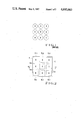
FIG. 1 shows a screen surface of a conventional color display device of this type. The circles represent display surfaces of single-color fluorescent display tubes. Reference symbols R, G, and B denote red, green, and blue, respectively. Three each of red, green, and blue fluorescent display tubes, a total of nine tubes, are used to constitute a 3 (rows)×3 (columns) matrix. A conventional color display device of this matrix arrangement has a low total resolution due to predetermined spaces between adjacent tubes. In addition, the numbers of parts and manufacturing steps are large, resulting in inconvenience.
SUMMARY OF THE INVENTION
It is an object of the present invention to provide a fluorescent display tube for a light source wherein the conventional problems can be solved, the resolution of a large-screen color display can be increased, and the manufacturing cost can be reduced.
In order to achieve the above object of the present invention, there is provided a fluorescent display tube comprising: an envelope constituted by a front panel, a rear panel, and a side panel, at least the front panel being able to transmit light therethrough; a plurality of phosphor screens formed on an inner surface of the front panel to constitute a matrix in a first direction and in a second direction perpendicular to the first direction; a plurality of anodes, respectively arranged around the phosphor screens, for accelerating electron beams; a plurality of cathodes, respectively corresponding to the phosphor screens and supported to float from an inner surface of the rear panel, for emitting the electron beams; plate-like control grids which are respectively arranged between the phosphor screens and the cathodes arranged in the first direction, and which have apertures for transmitting the electron beams from the cathodes to the phosphor screens; and stripe-like back electrodes which oppose the cathodes aligned on the inner surface of the rear panel along the second direction, wherein voltages applied to the control and back electrodes are higher or lower than those applied to the cathodes, thereby controlling light emission of the phosphor screens.
BRIEF DESCRIPTION OF THE DRAWINGS
FIG. 1 is a schematic view for explaining a color display device using conventional fluorescent display tubes for a light source;
FIG. 2 is a front view of a fluorescent display tube for a light source according to an embodiment of the present invention;
FIG. 3 is a sectional view of the display tube in FIG. 2 taken along the line III--III thereof; and
FIG. 4 is a perspective view showing part of the display tube in FIGS. 2 and 3.
DETAILED DESCRIPTION OF THE PREFERRED EMBODIMENT
The present invention will be described in detail with reference to the accompanying drawings.
FIG. 2 represents an illustration of a front display screen of a fluorescent display tube for a light source according to an embodiment of the present invention; FIG. 3 is a sectional view thereof taken along the line III--III thereof; and FIG. 4 is a perspective view showing part thereof. Referring to FIGS. 2 to 4, an envelope 1 is constituted by a glass front panel 2, a glass rear panel 3, and a glass side panel 4, which form a box-like shape. The envelope 1 is kept in vacuum. Phosphor screens 51,1, 51,2, . . . 53,3 of red, green, and blue phosphors are formed on the inner surface of the front panel 2 to constitute a matrix, as shown in FIG. 2. The phosphor screens are close to each other. Reference letters R, G, and B in FIG. 2 represent red, green, and blue, respectively. A plurality of accelerating anodes 61, 62, . . . are arranged corresponding to the boundaries between adjacent ones of phosphor screens 51,1 to 53,3. The anodes 61, 62, . . . are applied with a high voltage through an external terminal 16. Electron-emitting cathodes 71,1 to 73,3, respectively corresponding to the phosphor screens 51,1 to 53,3, are arranged in a matrix form in the same manner as the phosphor screens. Each of the cathodes 71,1 to 73,3 is supported between a pair of supports 17a and 17b fixed on the rear panel 3. An indirect heating type cathode prepared by coating an oxide on an Ni sleeve, or a direct heating type cathode prepared by coating an oxide on tungsten or the like can be used as each of the cathodes 71,1 to 73,3.
Discrete row selection control grids 81 to 83 are arranged between the cathode electrodes and the phosphor screens of the respective matrix rows. Each of the control grids 81 to 83 has electron beam apertures 91 to 93 for transmitting electron beams 11 as nonfocused beams from corresponding ones of the cathodes 71,1 to 73,3 to the corresponding phosphor screens 51,1 to 53,3.
Stripe-like three column selection back electrodes 101 to 103 are formed on the inner surface of the rear panel 3 so as to correspond to the columns of the matrix constituted by the cathodes 71,1 to 73,3. The back electrodes 101 to 103 are formed by conductive layers of Ag or the like. A negative and 0 V or a positive voltage of several volts, with respect to the potential at the cathodes 71,1 to 73,3, are applied to the back electrodes 101 to 103 to control the electron beams 11 emitted from the cathodes 71,1 to 73,3. Reference numeral 12 in FIG. 3 denotes lead pins as external terminals for leading the cathode, grid and back electrodes 71,1 to 73,3, 81 to 83, and 101 to 103 outside, through the back panel 3.
The basic operation of the arrangement described above will now be described. Assume that the back electrode 101 is kept negative with respect to the potential at the cathodes 71,1, 72,1, and 73,1. In this case, the electrons from the cathodes 71,1, 72,1, and 73,1 corresponding to the back electrode 101 are not supplied to the control grids 81 to 83 and the anode 61, and the cutoff state is obtained. If 0 V or a positive voltage of several volts, with respect to the potential at the cathodes 71,1 to 73,3, is applied to the back electrode 101, the electron beams 11 from the cathodes 71,1, 72,1, and 73,1 are supplied toward the control grids 81 to 83. For example, if the control grid 81 is negative with respect to the cathodes 71,1 to 73,3, the electron beam 11 cannot pass through the aperture 91 or reach the corresponding anode 61, and the phosphor screen 51,1 cannot emit light. However, if the control grid 81 is positive with respect to the cathodes 71,1 to 73,3, the electron beam 11 can pass through the corresponding aperture 91 to emit light from the phosphor screen 51,1. The above operation can also be applied to the back electrodes 102 and 103 and the control grids 82 and 83. By selectively driving the control grids 81 to 83 and the back electrodes 101 to 103, i.e., by performing dynamic driving thereof, the phosphor screens 51,1 to 53,3 at the intersections of the control grids and the back electrodes can be arbitrarily driven.
In the above embodiment, the number of phosphor screens is 3×3. However, the total number is not limited to 9. In addition, the number of phosphor colors need not be limited to three.
According to the present invention as described above, a composite fluorescent display tube for a light source incorporating a plurality of pixels in a single vacuum envelope can have a higher resolution since the space between adjacent pixels can be reduced. In addition, the numbers of parts and manufacturing steps can be reduced. At the same time, the structure of the display tube can be simplified. The display tube can be effectively applied to a large-screen display device, providing many practical advantages.

Claims (4)

What is claimed is:
1. A fluorescent display tube comprising:
an envelope constituted by a front panel, a rear panel, and a side panel, at least said front panel being able to transmit light therethrough;
a plurality of phosphor screens formed on an inner surface of said front panel to constitute a matrix in a first direction and in a second direction perpendicular to the first direction;
a plurality of anodes, respectively arranged around said phosphor screens, for accelerating electron beams;
a plurality of cathodes, respectively corresponding to said phosphor screens and supported to float from an inner surface of said rear panel, for emitting the electron beams;
plate-like control grids which are respectively arranged between said phosphor screens and said cathodes arranged in the first direction, and which have apertures for transmitting the electron beams from said cathodes to said phosphor screens; and
stripe-like back electrodes which oppose said cathodes aligned on said inner surface of said rear panel along the second direction,
wherein voltages applied to said control and back electrodes are higher or lower than those applied to said cathodes, thereby controlling light emission of said phosphor screens.
2. A tube according to claim 1, wherein said phosphor screens have a square shape and are arranged close to each other.
3. A tube according to claim 1, wherein said phosphor screens are constituted by red, green, and blue phosphor screens, which are provided in the same number.
4. A tube according to claim 1, wherein each of said cathodes is suspended to override a corresponding one of said stripe-like back electrodes through two support members fixed on said inner surface of said rear panel.
US06/880,139 1985-07-08 1986-06-30 Fluorescent display tube for light source Expired - Lifetime US4692663A (en)

Applications Claiming Priority (2)

Application Number Priority Date Filing Date Title
JP60148215A JPH0640474B2 (en) 1985-07-08 1985-07-08 Display tube for light source
JP60-148215 1985-07-08

Publications (1)

Publication Number Publication Date
US4692663A true US4692663A (en) 1987-09-08

Family

ID=15447843

Family Applications (1)

Application Number Title Priority Date Filing Date
US06/880,139 Expired - Lifetime US4692663A (en) 1985-07-08 1986-06-30 Fluorescent display tube for light source

Country Status (5)

Country Link
US (1) US4692663A (en)
EP (1) EP0217003B1 (en)
JP (1) JPH0640474B2 (en)
CA (1) CA1257638A (en)
DE (1) DE3674523D1 (en)

Cited By (3)

* Cited by examiner, † Cited by third party
Publication number Priority date Publication date Assignee Title
US4970430A (en) * 1988-03-31 1990-11-13 Ise Electronics Corporation Fluorescent display apparatus
US4972116A (en) * 1988-03-15 1990-11-20 Ise Electronics Corporation Light source display tube
US5036247A (en) * 1985-09-10 1991-07-30 Pioneer Electronic Corporation Dot matrix fluorescent display device

Families Citing this family (11)

* Cited by examiner, † Cited by third party
Publication number Priority date Publication date Assignee Title
JPS6420665U (en) * 1987-07-28 1989-02-01
JPH01100854A (en) * 1987-10-12 1989-04-19 Mitsubishi Electric Corp Fluorescent character display
JPH0673264B2 (en) * 1988-03-15 1994-09-14 三菱電機株式会社 Manufacturing method of anode electrode in light source display tube
JPH0762995B2 (en) * 1988-03-31 1995-07-05 三菱電機株式会社 Display tube for light source
KR0125090B1 (en) * 1988-03-29 1997-12-11 오가 노리오 Fluorescent tube
JPH0711950B2 (en) * 1988-03-31 1995-02-08 三菱電機株式会社 Display tube for light source
US5126620A (en) * 1988-12-19 1992-06-30 Mitsubishi Denki Kabushiki Kaisha Display element
JPH02177241A (en) * 1988-12-28 1990-07-10 Furukawa Electric Co Ltd:The Fluorescent character display panel
JP2981751B2 (en) * 1989-03-23 1999-11-22 キヤノン株式会社 Electron beam generator, image forming apparatus using the same, and method of manufacturing electron beam generator
JPH053006A (en) * 1991-06-25 1993-01-08 Mitsubishi Electric Corp Light emitting element
JP2804392B2 (en) * 1991-07-16 1998-09-24 三菱電機株式会社 Light emitting device and manufacturing method thereof

Citations (4)

* Cited by examiner, † Cited by third party
Publication number Priority date Publication date Assignee Title
US2956194A (en) * 1957-10-04 1960-10-11 Philips Corp Electron tube for the optical indication of an electrical magnitude
US4156239A (en) * 1976-07-16 1979-05-22 Canon Kabushiki Kaisha Display device
US4341980A (en) * 1979-09-05 1982-07-27 Tokyo Shibaura Denki Kabushiki Kaisha Flat display device
US4633134A (en) * 1983-09-22 1986-12-30 Futaba Denshi Kogyo Kabushiki Kaisha Color fluorescent display device having anode conductors in zig-zag pattern

Family Cites Families (4)

* Cited by examiner, † Cited by third party
Publication number Priority date Publication date Assignee Title
US4472658A (en) * 1980-05-13 1984-09-18 Futaba Denshi Kogyo Kabushiki Kaisha Fluorescent display device
JPS5737207A (en) * 1980-08-19 1982-03-01 Nippon Telegr & Teleph Corp <Ntt> Detecting mechanism for projection part on recording medium
GB2124825B (en) * 1982-08-06 1986-03-26 English Electric Valve Co Ltd Cathodoluminescent display arrangements
JPH0612657B2 (en) * 1983-07-30 1994-02-16 ソニー株式会社 Fluorescent display device

Patent Citations (4)

* Cited by examiner, † Cited by third party
Publication number Priority date Publication date Assignee Title
US2956194A (en) * 1957-10-04 1960-10-11 Philips Corp Electron tube for the optical indication of an electrical magnitude
US4156239A (en) * 1976-07-16 1979-05-22 Canon Kabushiki Kaisha Display device
US4341980A (en) * 1979-09-05 1982-07-27 Tokyo Shibaura Denki Kabushiki Kaisha Flat display device
US4633134A (en) * 1983-09-22 1986-12-30 Futaba Denshi Kogyo Kabushiki Kaisha Color fluorescent display device having anode conductors in zig-zag pattern

Cited By (3)

* Cited by examiner, † Cited by third party
Publication number Priority date Publication date Assignee Title
US5036247A (en) * 1985-09-10 1991-07-30 Pioneer Electronic Corporation Dot matrix fluorescent display device
US4972116A (en) * 1988-03-15 1990-11-20 Ise Electronics Corporation Light source display tube
US4970430A (en) * 1988-03-31 1990-11-13 Ise Electronics Corporation Fluorescent display apparatus

Also Published As

Publication number Publication date
DE3674523D1 (en) 1990-10-31
CA1257638A (en) 1989-07-18
EP0217003A1 (en) 1987-04-08
EP0217003B1 (en) 1990-09-26
JPH0640474B2 (en) 1994-05-25
JPS6210849A (en) 1987-01-19

Similar Documents

Publication Publication Date Title
US4692663A (en) Fluorescent display tube for light source
US5801485A (en) Display device
US7045947B2 (en) Vacuum display device
US6072272A (en) Color flat panel display device
US5055744A (en) Display device
JP3211271B2 (en) Light emitting element
US4972116A (en) Light source display tube
US4935670A (en) Image display device
JPH0676766A (en) Field radiant display
JP2587314B2 (en) Light source tubes for imaging devices
JPH053005A (en) Light emitting element
JP2778448B2 (en) Driving method of electron gun and cathode ray tube
JPH06111736A (en) Light emitting element
JPH01235152A (en) Display tube for light source
JPS6129056A (en) Dot matrix fluorescent character display tube
JP2833475B2 (en) Field emission fluorescent tube and driving method thereof
JP2751192B2 (en) Fluorescent display tube
JP2893358B2 (en) Display tube for light source
US6911782B2 (en) Field emission display with separated upper electrode structure
JPH0577141B2 (en)
JPH04267039A (en) Display tube for light source
JPH06119914A (en) Light emitting element
JPH01253148A (en) Display tube for light source
JPH06333518A (en) Light-emitting device
JPH01235150A (en) Display tube for light source

Legal Events

Date Code Title Description
AS Assignment

Owner name: ISE ELECTRONICS CORPORATION, 700, AZA-WADA, UENO-C

Free format text: ASSIGNMENT OF ASSIGNORS INTEREST.;ASSIGNORS:KOBAYASHI, MASAAKI;OKUBO, YOSIYUKI;TATSUDA, KAZUNORI;REEL/FRAME:004574/0095

Effective date: 19860606

STCF Information on status: patent grant

Free format text: PATENTED CASE

FEPP Fee payment procedure

Free format text: PAYOR NUMBER ASSIGNED (ORIGINAL EVENT CODE: ASPN); ENTITY STATUS OF PATENT OWNER: LARGE ENTITY

FPAY Fee payment

Year of fee payment: 4

FPAY Fee payment

Year of fee payment: 8

FPAY Fee payment

Year of fee payment: 12

AS Assignment

Owner name: NORITAKE ITRON CORPORATION, JAPAN

Free format text: CHANGE OF NAME;ASSIGNOR:ISE ELECTRONICS CORPORATION;REEL/FRAME:013280/0860

Effective date: 20020401