US4437182A - Method and apparatus for interleaving control signals - Google Patents
Method and apparatus for interleaving control signals Download PDFInfo
- Publication number
- US4437182A US4437182A US06/224,337 US22433781A US4437182A US 4437182 A US4437182 A US 4437182A US 22433781 A US22433781 A US 22433781A US 4437182 A US4437182 A US 4437182A
- Authority
- US
- United States
- Prior art keywords
- control signals
- channel
- signals
- channels
- transmission
- Prior art date
- Legal status (The legal status is an assumption and is not a legal conclusion. Google has not performed a legal analysis and makes no representation as to the accuracy of the status listed.)
- Expired - Fee Related
Links
Images


Classifications
-
- H—ELECTRICITY
- H04—ELECTRIC COMMUNICATION TECHNIQUE
- H04J—MULTIPLEX COMMUNICATION
- H04J3/00—Time-division multiplex systems
- H04J3/02—Details
- H04J3/12—Arrangements providing for calling or supervisory signals
Definitions
- This relates to a method and apparatus for operating a time division multiplexer (TDM) system and, in particular, a method and apparatus for control signaling in such a system.
- TDM time division multiplexer
- a transmitter samples pulse signals of relatively low pulse repetition frequency from various data sources or channels and interleaves them with one another to form an aggregate data stream that is transmitted by a high speed aggregate channel to a remote receiver.
- the TDM transmitter inserts the signals representative of a single bit or a single character in a single time slot in the aggregate data stream and interleaves the signals from different channels on a bit-by-bit or character-by-character basis so that adjacent time slots contain signals from different channels.
- different size blocks of signals can be used if desired.
- the individual bits or characters are separated from one another and allocated to various low frequency data channels similar to those at the transmitter.
- the transmitter interleaves the signals from the various data channels in accordance with a fixed schedule which it repeats endlessly and the receiver uses the same schedule to decode the data stream.
- Each cycle of the schedule is called a frame or an aggregate frame.
- each frame ordinarily includes synchronization signals called frame sync words and various control signals, both for individual channels and for the entire TDM system.
- the synchronization and control signals take up a small portion (less than 5%) of the total frame which is referred to as the overhead.
- it is customery to sample the data channels in a fixed pattern which is repeated numerous times within each frame. Each such cycle of repetition is called a subframe.
- the protocol used in many TDMs is to transmit a change in the control signals for a channel in the next available time slot after a change has occurred. If a time slot becomes available for transmission and there are no changes to be transmitted, a counter is incremented and the incremented value is used to select a channel whose control signals are transmitted.
- a method and apparatus have been devised to ensure that control signals from every data channel are transmitted periodically regardless of any change in these control signals.
- Apparatus is provided for counting the control signals that are transmitted. At a fixed interval, such as once in every eight control signal transmissions, the apparatus defers the transmission of a new set of control signals in favor of a set of control signals selected systematically from the available data channels.
- the apparatus comprises a counter for counting the number of control signals transmitted, decision logic for determining when it is time to transmit a set of control signals regardless of any change in the control signals, and circuitry for selecting the channel whose signals are to be transmitted. Further, the apparatus provides equipment for determining when the control signals for a particular channel have changed and for transmitting such signals with suitable error checking. Finally, the apparatus provides means for interleaving the two flows of control signals without loss of the control signals which have changed.
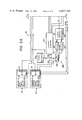
- FIG. 1 is a block diagram depicting an illustrative embodiment of a frame generator of the prior art which may be used in the practice of my invention
- FIG. 2, consisting of FIGS. 2A and 2B is a block diagram of an illustrative embodiment of portion of a TDM transmitter modified in accordance with the invention
- FIG. 3 is a flow chart useful in understanding the operation of a first portion of the apparatus of FIG. 2;
- FIG. 4 is a flow chart useful in understanding the operation of a second portion of the apparatus of FIG. 2;
- FIGS. 5 and 6 are schematic illustrations of certain details of the apparatus of FIG. 2;
- FIG. 7 is a block diagram of an illustrative embodiment of a TDM receiver for receiving signals transmitted by the apparatus of FIG. 2.
- FIGS. 1, 2 and 3 Simplified block diagrams of an illustrative TDM system, a TDM transmitter and a TDM receiver are set forth in FIGS. 1, 2 and 3 respectively, of U.S. Pat. No. 3,632,882 for "Synchronous Programmable Mixed Format Time Division Multiplexer," which is incorporated herein by reference.
- a plurality of pulse data sources or channels A-X are connected by transmitter multiplexer 100 in time-division multiplex format via a conventional transmission system 101 to a receiver demultiplexer 102 where the interleaved data signals are separated and delivered to appropriate data sinks A-X.
- each station in a TDM system usually comprises both a transmitter and a receiver for two way communication between the stations of the system.
- the channel select signals may be stored in a programmable read only memory and the signals may be read out by accessing the individual addresses of the memory serially using a binary counter.
- a frame generator 10 might comprise a recycling binary counter 20, a memory 30 and a decoder 40.
- the memory might be a 1KX8 bit memory with ten parallel input lines 32, a 10-line-to-1024 line decoder 34, a read only memory matrix 36 having 1,024 address lines to memory locations which are addressed one at a time and eight parallel binary output lines 38.
- the signal on the ten input lines is decoded to activate a single address line to the memory matrix.
- These output lines are then applied to decoder 40 which converts a parallel binary signal on its eight input lines to an output on one of as many as 256 output lines.
- Such gates are shown as elements 200A-200Z and 201A-201Z in the transmitter multiplexer 100 depicted in FIG. 2 of the U.S. Pat. No. 3,632,882 and elements 300A-300X and 301A-301X in receiver multiplexer 102 of FIG. 3 of that patent.
- Other output lines are available to enable gates for control and synchronization signaling.
- Each data channel uses a set of control signals for signaling between the customer's terminals at either end of the channel.
- These control signals typically are one or more of the standard EIA signals including request to send, clear to send, data set ready, data terminal ready and the like.
- Illustrative TDM apparatus 110 for controlling the transmission of control signals in accordance with the invention is depicted in block diagram form in FIG. 2. As will be apparent, this apparatus interleaves the signals from the different data channels on a bit-by-bit basis.
- Apparatus 110 comprises a control scanner 120, a frame generator 130, a data signal source 140, an addressing means 150, a control signal source 160, a transmission means 170, a first signal bus 180 and a second signal bus 185.
- the capacity of the apparatus of FIG. 2 is large enough to accommodate up to 64 separate data channels; and the modification of the apparatus to accommodate other numbers of channels will be obvious.
- FIG. 2 does not depict numerous elements of a TDM transmitter which are not part of this invention. For convenience the number of lines in the connection between blocks is represented schematically by the number followed by a slash mark.
- the invention may be practiced with any type of frame generator 130 which produces a multiplicity of output signals, some of which are used to select data channels for transmission and others of which are used to initiate control and/or synchronization signaling.
- frame generator 130 is similar to that of FIG. 1.
- Specific details of a frame generator which preferably is used with the invention are set forth in the above referenced application "Automatic Framing in Time Division Multiplexer".
- a portion of the contents of the memory of frame generator 130 is set forth in Table 1.
- the eight output lines of frame generator 130 are coupled to control scanner 120, and to data signal source 140. Six of the lines from generator 130 are connected to means 153 for determining the largest channel number. One of the lines from frame generator 130 is also connected to a transmit data multiplexer 178 in transmission means 170.
- Data signal source 140 comprises the 64 individual channels that are served by the TDM and a multiplexer 142 which selects for transmission one bit of the data present on one channel in accordance with the channel select signal supplied from frame generator 130. Further details of an illustrative multiplexer 142 are disclosed in U.S. Pat. No. 3,632,882. As will be apparent, to control channel select gates 200A-200Z and 201A-201Z of the multiplexer of the '882 patent, it will be necessary to decode the address signals supplied from frame generator 130 of the present invention.
- Addressing means 150 is used to address individually each one of the 64 channels which may be connected to the TDM. It comprises first and second counters 151, 152, means 153 for generating the largest channel number, a control address multiplexer 154, a row select decoder 156 and a column select decoder 158.
- Generating means 153 comprises latches and a comparator which read the channel select signals from frame generator 130 and determine the number of the highest channel. This number is loaded into counters 151, 152 at the beginning of each cycle of the counter. Under the control of control scanner 120, multiplexer 154 uses the count on either counter 151 or counter 152 to address decoders 156, 158.
- counters 151 and 152 each have a capacity of 64 and have six output lines by which their instantaneous count is transferred to control address multiplexer 154. As indicated in FIG. 2, three of these output lines are used to address decoder 156 and the other three are used to address decoder 158.
- Each decoder is a 1-of- 8 decoder which produces an output signal on one of eight lines in accordance with the binary signal presented in parallel on its three input lines.
- the eight output lines from decoder 156 are row select lines and those from decoder 158 are column select lines.
- Counters 151, 152 may be implemented with pairs of 169-type synchronous counters; and multiplexer 154 may be a pair of 157-type quad 2-input multiplexers.
- Generating means 153 may use 377-type octal D flip-flops and a pair of 85-type 4 bit comparators.
- Decoders 156, 158 may be 138-type 1-of-8 decoders.
- Control signal source 160 comprises the individual channels that are multiplexed by the TDM and a multiplexer 162 which selects for transmission the control signals present on one channel in accordance with the address supplied on the row select and column select address lines from decoders 146, 148.
- the multiplexer may be similar to that described in U.S. Pat. No. 3,632,882.
- four control signal lines are used in the preferred embodiment of the invention, permitting the use of up to 16 binary coded control signals or as many as four uncoded signals.
- Transmission means 170 comprises a next control latch 172, a control latch 174, a control bit multiplexer 176 and transmit data multiplexer 178.
- transmit data multiplexer 178 transmits a bit of data supplied from data source 140.
- multiplexer 178 transmits one bit of that signal supplied from control bit multiplexer 176.
- each control signal consists of ten bits, four of which are channel control signals and six of which specify the address of the channel to which the controls pertain.
- control signal that is being transmitted is stored in control latch 174 and read one bit at a time by control bit multiplexer 176 in response to CONTROL select signals that are generated by frame generator 130 and used by scanner 120 to control the operation of multiplexer 176. While the signal in control latch 174 is being transmitted, the control bits and associated channel address of the next control signal are loaded into the next control latch 172 under control of scanner 120. Latches 172, 174 may be implemented with pairs of 377-type octal D flip-flops. Multiplexer 176 can be a pair of 251 type 8-input multiplexers and multiplexer 178 can be a 153-type dual 4-line to 1-line multiplexer.
- FIG. 3 An illustrative flow chart for the operation of transmission means 170 is set forth in FIG. 3.
- each control signal is transmitted twice to protect against transmission errors.
- a bit counter (not shown in FIG. 2) is used to record the number of bits in the control signal that have been transmitted; and a flag bit which is set before any part of the signal is transmitted is used to determine whether the signal has been transmitted once or twice.
- Each time frame generator 130 produces a time slot in which a control signal is to be transmitted, the steps depicted in FIG. 3 are executed immediately under control of hard-wired logic in scanner 120.
- scanner 120 causes multiplexer 176 to read the next control bit stored in latch 174 and to forward that bit to multiplexer 178 for transmission.
- the bit counter is then decremented by one.
- the control scanner tests to determine if the contents of the bit counter equals zero. If it does not, there is no further operation to be performed and the scanner waits for the next time slot in which a control signal is to be transmitted. If the bit counter equals zero, the scanner tests to determine if the first transmission bit has been set.
- the scanner clears the transmission bit; and when the next control signal time slot is produced, it loads the bit counter to nine. If the first transmission bit has not been set, the complete control signal has been transmitted twice and the transmission means is ready to receive a new control signal. Thus, the scanner sets the first transmission bit as well as a first flag bit which indicates that a control signal and address has just been loaded from next control latch 172 into control latch 174. The scanner then performs the loading operation represented by the first flag bit it just set; and finally, when the next control signal time slot is produced, it loads the bit counter to nine.
- New control signals and addresses are loaded by scanner 120 into next control latch 172 by a second sequence of operations depicted in FIG. 4.
- the purpose of this procedure is to detect the change in the control signals in any channel, to load the new set of control signals and the address for that channel into next control latch 172 and to ensure that the polled control signals from each channel are transmitted periodically regardless of whether there has been any change in their status.
- the left hand side of the flow chart of FIG. 4 details the steps performed by scanner 120 to locate a channel where the control signals have changed and to store the new control signals and their channel address in the next control latch.
- the right hand side of the flow chart of FIG. 4 details the tests performed by scanner 120 to ensure that each channel's control signals are transmitted periodically. Up to seven updated control signals may be transmitted in a row. The eighth control signal to be transmitted, however, must be sent from a polled channel that is selected regardless of any change in the control signal.
- Counter 151 is used to address the data channels to access updated control signals; and counter 152 is used to address the data channels to access the polled control signals.
- a third counter (not shown in FIG. 2) is used to determine when a polled control signal must be interleaved with the updated control signals.
- a change in a control signal is indicated to control scanner 120 by the fact that the signal on first bus 180 goes low.
- This signal is, in essence, an interrupt signal such as that commonly used in prior art TDMs to signify that a channel needs servicing. If the first, second and third flag bits are not set, the scanner strobes counter 151 and address multiplexer 154 so that the six bit address then in counter 151 addresses one of the 64 channels serviced by the TDM. This address is retained in multiplexer 154. Scanner 120 then decrements counter 151. If the control signals associated with the channel that is addressed are the control signals that have changed, second bus 185 will go low.
- next control latch 172 both the address on the output lines from multiplexer 154 and the control signals from the channel that is addressed.
- the scanner sets a third flag bit to prevent the contents of next control latch 172 from being over-written.
- transmission means 170 completes the transmission of the signal then in control latch 174, it sets the first flag bit and loads the signal in next control latch 172 into control latch 174.
- control scanner 120 detects the first flag bit, its operation branches to the right hand side of FIG. 4. In that branch it initially clears the first and second flag bits and disables counter 151. It then tests to determine if the third flag bit is set. If that flag is not set, the signal that was just loaded into control latch 174 was a polled signal and there is no pressing need to transmit another polled signal before seven updated signals are next transmitted.
- scanner 120 decrements counter 152 by one to access the next polled channel, loads the interleave counter and clears the third flag bit which protects the contents of next control latch 172 from being over-written. It then strobes counter 152 and multiplexer 154 to address the channel whose address is stored in counter 152. The control signals for that channel as well as their address are then loaded into next control latch 172. As a precaution, the scanner tests to determine if second bus 185 has gone low. If it has not, the control signals that were just loaded into the next control latch are polled signals. If, however, the bus has gone low, then the signals loaded in the next control latch are updated control signals; and scanner 120 sets a second flag bit to protect these signals from being over-written. Scanner 120 then returns to the test procedure in accordance with the left hand side of the flow chart of FIG. 4.
- scanner 120 will write this new set of updated control signals over the contents of next control latch 172 in accordance with the procedures set forth on the left hand side of FIG. 4. Otherwise, the control signals for the channel addressed by counter 152 will be present in next control latch 172 when transmission means 170 completes transmission of the signal in control latch 174 and transfers the contents of the next control latch 172 to control latch 174.
- control scanner 120 tests the status of the interleave counter. If the counter has not reached zero, it decrements the counter and clears the third flag bit.
- scanner 120 sets the second flag bit before loading the interleave counter and clears the third flag bit. It then strobes counter 152 and multiplexer 154 to address a polled channel and stores the control signal and its address in next control latch 172. Since in this case the second flag bit is set, these contents cannot be over-written and will be the next control signal transmitted by the TDM. As a result, in at least one case out of eight, a polled control signal is transmitted.
- scanner control 120 specific hardware and software implementations of this scanning logic will be apparent to those skilled in the art.
- An illustrative hard-wired implementation of the above described features of scanner control 120 is set forth in FIGS. 5 and 6.
- the apparatus of FIG. 5, which is used to execute the flow chart of FIG. 3, comprises a control bit detection logic 210, an end-of-frame (EOF) detection logic 215, a counter 220, a first D-type flip-flop 230, an AND gate 240, an inverter 245, an exclusive OR (XOR) gate 250, and an OR gate 255. It also includes next control latch 172, control latch 174 and control bit multiplexer 176 which are the same devices as depicted in FIG. 2B. In addition, a second D-type flip-flop 260 and an AND gate 265 shown at the bottom of FIG. 6 are used in implementing the flow chart of FIG. 3.
- the bubbles at the inputs or outputs of many of the elements of FIGS. 5 and 6 indicate signal inversion (or negation).
- AND gates 240 and 265 and OR gate 255 are drawn as OR gates and AND gates, respectively, which are negated at both their input and output.
- Counter 220, flip-flops 230, 260 and latches 172, 174 are all clocked together by a common clock signal.
- Counter 220 is a conventional 169-type counter having count-enable input terminals P and T, a clock terminal CK, output terminals Q, a carry lookahead terminal CRY, and a load terminal L.
- the counter is enabled by a low signal on line 212 and is advanced by one for each clock signal received while it is enabled.
- whether the count stored in the counter is incremented or decremented is a matter of design choice.
- counter 220 has been decremented from a count of nine.
- the signal on line 214 from the carry terminal CRY is high except when the counter reaches zero.
- Output lines 216 from terminals Q strobe control bit multiplexer 176 so as to read out one at a time the ten control bits in control latch 174 in accordance with the count stored in the counter.
- Flip-flop 230 stores the first transmission bit. When this bit is set, the output terminal Q of flip-flop 230 is high; otherwise it is low.
- Flip-flop 260 stores the first flag bit. When this bit is set, the output terminal Q of flip-flop 260 is low; otherwise it is high.
- Control bit detection logic 210 and end of frame logic 215 monitor the output of frame generator 130. Whenever the frame generator reaches a time slot allocated to a control bit, it produces a CONTROL select signal such as those shown in Table 1. In the absence of a CONTROL select signal, the output of detection logic 210 on line 212 is high. As a result, the counter operation is disabled and clock signals applied to the CK terminal do not affect the count. When detection logic 210 senses a CONTROL select signal, its output signal goes low, thereby enabling counter 220. As a result, the counter is advanced by one upon receipt of the next clock signal.
- the signal on line 214 from the carry terminal CRY remains high.
- the signal on line 257 from OR gate 255 is high thereby disabling control latch 174.
- the signal on line 257 is also applied to AND gate 265 shown at the bottom of FIG. 6.
- AND gate 265 operates so as to apply to input terminal D of flip-flop 260 the signal on line 412.
- the output signal from flip-flop 260 is ordinarily high and the signal on line 412 will ordinarily be high. In these circumstances, there will be no change in the output of flip-flop 260 upon receipt of the next clock signal.
- the circuitry waits for the next CONTROL select signal to be generated by frame generator 130.
- a low signal on line 214 is also inverted by inverter 245 and applied to XOR gate 250. If the output of flip-flop 230 is low (i.e., the transmission bit is not set), the output of XOR gate 250 is high and a high signal is applied to the input of flip-flop 230. When the next clock signal is received, this causes the output of flip-flop 230 to go high. Thus, if the first transmission bit is not set in flip-flop 230, upon receipt of the next clock signal the first transmission bit is set in flip-flop 230, the first flag bit is set in flip-flop 260 and the control signal and its address are loaded from next control latch 172 into control latch 174.
- the first transmission bit is set so that the output of flip-flop 230 is high, the signal on line 257 from OR gate 255 will be high regardless of any change in the signal on line 214 from carry terminal CRY. As a result, no change will take place in the signal applied to control latch 174 or flip-flop 260. However, when the signal on line 214 from terminal CRY goes low, both input terminals to XOR gate 250 will be high, causing the signal applied to the input to flip-flop 230 to go low. When the next clock signal is received by flip-flop 230, this causes the output of flip-flop 230 to go low, thereby clearing the first transmission bit.
- line 214 is also applied to AND gate 240.
- a low signal is produced on an input lead 216 to load terminal L of counter 210. This signal reloads the counter to its initial value of nine upon receipt of the next clock signal.
- Counter 220 is also reloaded in the same fashion when EOF detection logic 215 detects an end of frame (EOF) signal in the signals produced by frame generator 130.
- EEF end of frame
- FIG. 6 Illustrative apparatus for executing the flow chart of FIG. 4 is shown in FIG. 6.
- This apparatus comprises flip-flop 260, which has been described above, D-type flip-flops 280, 310 and 370, a counter 400 and extensive amounts of control logic for controlling the signals stored in the flip-flops, the resetting of the flip-flops and the generation of output control signals to the transmitter.
- first and second counters 151, 152, multiplexer 154 and next control latch 172 which are the same as the devices of the same number shown in FIGS. 2A and 2B.
- flip-flop 260 stores the first flag bit. When this bit is set, the output terminal Q of flip-flop 260 is low; otherwise it is high.
- Flip-flop 280 stores the second flag bit and flip-flop 310 stores the third flag bit. When either of these bits is set, the output terminal Q of the flip-flop is low; otherwise it is high.
- Flip-flop 370 records the fact that first data bus 180 is low while the second and third flag bits are not set. When this condition is met, the output terminal Q of flip-flop 370 is high; otherwise it is low.
- Counter 400 is the interleave counter which is used to ensure that one out of every eight control signals transmitted is obtained from a polled channel regardless of any change in the control signal. Counter 400 is a conventional 169-type counter, the same as counter 220 of FIG.
- counter 400 is decremented from a count of seven.
- Counters 151, 152 and 400, latch 172 and flip-flops 260, 280, 310 and 370 are all clocked together by the same clock signal that is used to control the operation of the counter, flip-flops and latches depicted in FIG. 5.
- the circuit of FIG. 6 is operated in step with that of FIG. 5 by means of the signal on line 257 from OR gate 255.
- This signal is normally high, a signal which disables interleave counter 400 while enabling AND gates 265 and 270.
- the high signal on line 257 is also applied through OR gate 330 to line 332 which is connected to the enable terminal of counter 152.
- counter 152 is disabled.
- the signal on line 257 is also inverted by inverter 275 and applied by line 277 to OR gates 285 and 320 in the control logic for flip-flops 280 and 310, respectively.
- Bus 185 is high except when the output signals from multiplexer 154 address a data channel whose control signals have changed. Hence the signals on lines 342 and 347 from OR gates 340 and 345 are ordinarily high, thereby enabling AND gates 295, 315 and 380.
- the signal on output line 312 will be high, thereby enabling AND gate 315.
- the other input to AND gate 315 is line 347 which ordinarily is high because bus 185 is high.
- the signal on line 317 from AND gate 315 will be high, the signal on line 322 from OR gate 320 will likewise be high, the input to flip-flop 310 will be high, and the flip-flop will not change states when it is clocked.
- a high signal on line 322 will also be applied to AND gate 360 with the result that the signal on line 362 from AND gate 360 will be high when both the second and third flag bits are not set.
- This signal enables AND gate 365 so that when first bus 180 goes low a high signal is applied to the input of flip-flop 370 causing the output of the flip-flop to go high upon receipt of the next clock signal. Since the signal on line 272 from AND gate 270 is also high, this causes the signal on line 377 from the output of NAND gate 375 to go low.
- Line 377 is applied to the enable terminal of counter 151.
- the counter is enabled; and while it is enabled, it is decremented by one for each successive clock signal.
- multiplexer 154 uses the contents of counter 151 to address the channel address decoders 156, 158.
- counter 151 is decremented by one with each successive clock signal.
- AND gate 315 is disabled by the output signal so that the signal applied to the input to flip-flop 310 will remain low as long as the signal on line 257 is high.
- the low signal on line 322 is also applied to AND gate 360 to disable this gate and thereby disable AND gate 365 as well. This causes the input to flip-flop 370 to go low; and upon receipt of the next clock signal, the signal on line 372 from flip-flop 370 goes low, thereby disabling NAND gate 375.
- NAND gate 375 is disabled, the signal on line 377 goes high disabling counter 151.
- the high signal on line 377 is applied to OR gate 345 causing the signal on line 347 to go high once more. Since both inputs to AND gate 380 are now high, the signal on line 382 goes high thereby disabling the enable terminal of latch 172.
- the circuit executes the procedure illustrated in the right hand side of the flow chart of FIG. 4.
- the low signal on line 257 constitutes the first flag bit. It causes the signal on line 267 from AND gate 265 to flip-flop 260 to go low; and the first flag bit is set in flip-flop 260 upon receipt of the next clock signal.
- the low signal on line 257 is also applied to inverter 275, thereby producing a high signal on line 277 and on line 287. If line 404 is high, the output of AND gate 290 is also high. Since bus 185 is ordinarily high, the signal on line 342 from OR gate 340 is likewise high and the signal applied on line 297 to the input of flip-flop 280 is high. Upon receipt of the next clock signal, the output of flip-flop 280 will therefore go high, clearing any second flag bit.
- the high signal on line 277 is also applied through OR gate 320 to the input to flip-flop 310. Upon receipt of the next clock signal, the output of flip-flop 310 will also go high, clearing any third flag bit.
- the output of flip-flop 310 is tested by OR gate 330 for the presence of the third flag bit. If the third flag bit is not set, the output of flip-flop 310 is high, causing the signal on line 327 from inverter 325 to be low. As a result, when the signal on line 257 is also low, the signal on line 332 is low. This signal enables counter 152; and upon receipt of the next clock signal, counter 152 is decremented by one.
- the signal on output line 262 goes low, causing the output of multiplexer 154 to be the newly decremented count stored in counter 152.
- the low signal on line 262 disables AND gate 380, thereby producing a low signal on line 382. This signal enables the latch so as to store in latch 172 the control signals from the polled channel addressed by counter 152.
- control 420 When the buses are available, the output of control 420 is high causing the signal on line 412 from OR gate 410 to be high. Therefore, as soon as the signal on line 257 goes high, the signal on line 267 from AND gate 265 goes high; and upon receipt of the next clock signal, flip-flop 260 will again change state thereby clearing the first flag bit.
- the third flag bit is set when the signal on line 257 goes low, the signal on line 327 is high, causing the signal on line 332 to be high. As a result, counter 152 is disabled. If counter 400 has reached zero and the signal on line 404 is low, AND gates 290 and 395 are disabled and the signals on lines 292 and 408 are low. The low signal on line 408 enables the load terminal L of counter 400 so that the counter is reloaded upon receipt of the next clock signal. The signal on line 292 causes line 297 to be low and the clock signal which reloads counter 400 also causes the second flag bit to be set in flip-flop 280. As indicated above, this same clock signal clears the third flag bit, decrements counter 152, and stores in next control latch 172 the control signal and the address specified by counter 152.
- the channel addressed by counter 152 is one whose control signals had just changed. If this is the case, the signal on second bus 185 will go low when the channel is addressed. If this happens, the signal on line 342 goes low causing the signal on line 297 to be low. As a result, upon receipt of the next clock signal, the second flag bit will be set at flip-flop 280.
- FIG. 7 depicts an illustrative TDM receiver 510 for processing the signals received from a transmitter such as that of FIG. 2.
- this receiver is synchronous with the transmitter with which it is in communication. Under control of clock signals derived from the received signals, the receiver separates the control signals from the data signals as they are received on a bit-by-bit basis, reassembles the control signals, and routes the data signals and the control signals to their appropriate channels.
- Apparatus 510 comprises a first shift register 520, a data signal sink 530, data signal column select and row select decoders 534, 536, a second shift register 540, a latch 545, a comparator 550, a control signal sink 560, and control signal column select and row select decoders 564, 566.
- the apparatus further comprises a frame generator 570, control bit detection logic 575, end-of-frame (EOF) detection logic 580, data signal detection logic 585, a counter 590 and an AND gate 595 which function in similar fashion to frame generator 130, control bit detection logic 210, EOF detection logic 215, counter 220 and AND gate 240 of FIG. 5.
- EEF end-of-frame
- Counter 590 reaches zero on every tenth count producing an output on line 592 which enables latch 545 and reloads the counter.
- the apparatus also comprises an inverter 600 and an OR gate 605, which enable decoders 564, 566 on every twentieth count if the contents of latch 545 and comparator 550 are the same.
- FIG. 7 does not depict numerous elements of a TDM receiver which are not part of this invention.
- Frame generator 570 is substantially the same as frame generator 130 of FIG. 2 and produces the exact same sequence of output signals, some of which are used to route received signals to the data channels and others of which are used for routing of control and/or synchronization signals.
- Data signal sink 530 comprises the 64 individual channels that are served by the TDM and a demultiplexer 532 which routes a bit of received data to an individual channel in accordance with the channel select signal supplied from frame generator 570. Further details of an illustrative demultiplexer 532 are disclosed in U.S. Pat. No. 3,632,882.
- data signal detection logic 585 detects a data channel select signal in the output signal from frame generator 570, it enables column select and row select decoders 534, 536 to decode the address in the channel select signal.
- the output of decoders 534, 536 controls an array of channel select gates such as gates 300A-300X and 301A-301X of the demultiplexer of the '882 patent.
- Control signal sink 560 comprises the individual channels that are served by TDM and a demultiplexer 562 which routes a control signal to an individual channel in accordance with the address supplied from column select and row select decoders 564, 566.
- the demultiplexer may be similar to that described in U.S. Pat. No. 3,632,882.
- each control signal consists of ten bits and it is transmitted twice to ensure accuracy of transmission. Thus, ten bits must be shifted into register 540 to assemble a complete control signal therein; and two complete control signals are shifted through the register, one immediately after the other.
- column select and row select decoders 564, 566 are enabled and the address portion of the control signal stored in latch 545 is decoded by these decoders.
- the signal on the remaining four lines from latch 545 is the control signal which is routed by multiplexer 562 to the channel specified by the column select and row select decoders 564, 566.
- a transmitter such as shown in FIGS. 2A and 2B and a receiver such as shown in FIG. 7 are located at each station in a TDM communication system but transmit only or receive only stations may be used.
- Different techniques may be devised for interleaving the polled control signals with the updated control signals; and different ways for implementing such techniques, both in hardware and in software, will be apparent to those skilled in the art.
- the apparatus described provides for bit interleaving of the signals from the different channels, appropriate modification of the apparatus to provide for character interleaving or the interleaving of other size blocks of data will be apparent to those skilled in the art.
Abstract
Description
              TABLE 1
______________________________________
Memory Output Line
Location
       7     6      5   4   3    2   1   0    Function
______________________________________
395    0     0      0   0   0    0   0   1    CH1 Select
396    1     1      0   0   1    1   1   1    CONTROL
397    0     0      0   0   0    0   0   1    CH1 Select
398    0     0      0   0   0    0   1   0    CH2 Select
399    0     0      0   0   0    0   1   1    CH3 Select
400    0     0      0   0   0    1   0   0    CH4 Select
401    1     1      0   0   1    1   1   1    CONTROL
402    0     0      0   0   0    0   0   1    CH1 Select
403    0     0      0   0   0    1   0   1    CH5 Select
404    0     0      0   0   0    1   1   1    CH7 Select
405    0     0      0   0   1    0   0   1    CH9 Select
406    1     1      0   0   1    1   1   1    CONTROL
407    0     0      1   1   1    1   1   0    CH62 Select
408    0     0      1   1   1    1   1   1    CH63 Select
______________________________________
Claims (20)
Priority Applications (3)
| Application Number | Priority Date | Filing Date | Title |
|---|---|---|---|
| US06/224,337 US4437182A (en) | 1981-01-12 | 1981-01-12 | Method and apparatus for interleaving control signals |
| CA000393874A CA1179432A (en) | 1981-01-12 | 1982-01-11 | Method and apparatus for interleaving control signals |
| GB8200742A GB2092863B (en) | 1981-01-12 | 1982-01-12 | Method and apparatus for interleaving control signals |
Applications Claiming Priority (1)
| Application Number | Priority Date | Filing Date | Title |
|---|---|---|---|
| US06/224,337 US4437182A (en) | 1981-01-12 | 1981-01-12 | Method and apparatus for interleaving control signals |
Publications (1)
| Publication Number | Publication Date |
|---|---|
| US4437182A true US4437182A (en) | 1984-03-13 |
Family
ID=22840223
Family Applications (1)
| Application Number | Title | Priority Date | Filing Date |
|---|---|---|---|
| US06/224,337 Expired - Fee Related US4437182A (en) | 1981-01-12 | 1981-01-12 | Method and apparatus for interleaving control signals |
Country Status (3)
| Country | Link |
|---|---|
| US (1) | US4437182A (en) |
| CA (1) | CA1179432A (en) |
| GB (1) | GB2092863B (en) |
Cited By (4)
| Publication number | Priority date | Publication date | Assignee | Title |
|---|---|---|---|---|
| US4512015A (en) * | 1981-12-29 | 1985-04-16 | Fujitsu Limited | Digital time-division switch |
| US5182753A (en) * | 1990-03-20 | 1993-01-26 | Telefonaktiebolaget L M Ericsson | Method of transmitting signaling messages in a mobile radio communication system |
| US5537404A (en) * | 1992-12-29 | 1996-07-16 | International Business Machines Corporation | Switched circuit connection management over public data networks for wide area networks |
| US6744788B2 (en) * | 1998-09-23 | 2004-06-01 | Sony United Kingdom Limited | Multiplexing digital signals |
Families Citing this family (1)
| Publication number | Priority date | Publication date | Assignee | Title |
|---|---|---|---|---|
| GB2153634B (en) * | 1984-02-02 | 1987-03-25 | Plessey Co Plc | An arrangement for controlling switched speech or data communication in a communications exchange |
Citations (4)
| Publication number | Priority date | Publication date | Assignee | Title |
|---|---|---|---|---|
| US3588364A (en) | 1967-06-19 | 1971-06-28 | Nat Defense Canada | Adaptive encoder and decoder |
| US3959594A (en) | 1974-07-01 | 1976-05-25 | Gte Automatic Electric Laboratories Incorporated | Arrangement and method for the localized self-control of randomly allotted time slots to audio ports |
| US3961140A (en) | 1975-03-21 | 1976-06-01 | Bell Telephone Laboratories, Incorporated | Line switch controller for a time-division switching system |
| US4059731A (en) | 1977-02-01 | 1977-11-22 | Bell Telephone Laboratories, Incorporated | Signaling storage in digital channel banks |
-
1981
- 1981-01-12 US US06/224,337 patent/US4437182A/en not_active Expired - Fee Related
-
1982
- 1982-01-11 CA CA000393874A patent/CA1179432A/en not_active Expired
- 1982-01-12 GB GB8200742A patent/GB2092863B/en not_active Expired
Patent Citations (4)
| Publication number | Priority date | Publication date | Assignee | Title |
|---|---|---|---|---|
| US3588364A (en) | 1967-06-19 | 1971-06-28 | Nat Defense Canada | Adaptive encoder and decoder |
| US3959594A (en) | 1974-07-01 | 1976-05-25 | Gte Automatic Electric Laboratories Incorporated | Arrangement and method for the localized self-control of randomly allotted time slots to audio ports |
| US3961140A (en) | 1975-03-21 | 1976-06-01 | Bell Telephone Laboratories, Incorporated | Line switch controller for a time-division switching system |
| US4059731A (en) | 1977-02-01 | 1977-11-22 | Bell Telephone Laboratories, Incorporated | Signaling storage in digital channel banks |
Cited By (4)
| Publication number | Priority date | Publication date | Assignee | Title |
|---|---|---|---|---|
| US4512015A (en) * | 1981-12-29 | 1985-04-16 | Fujitsu Limited | Digital time-division switch |
| US5182753A (en) * | 1990-03-20 | 1993-01-26 | Telefonaktiebolaget L M Ericsson | Method of transmitting signaling messages in a mobile radio communication system |
| US5537404A (en) * | 1992-12-29 | 1996-07-16 | International Business Machines Corporation | Switched circuit connection management over public data networks for wide area networks |
| US6744788B2 (en) * | 1998-09-23 | 2004-06-01 | Sony United Kingdom Limited | Multiplexing digital signals |
Also Published As
| Publication number | Publication date |
|---|---|
| CA1179432A (en) | 1984-12-11 |
| GB2092863B (en) | 1985-01-23 |
| GB2092863A (en) | 1982-08-18 |
Similar Documents
| Publication | Publication Date | Title |
|---|---|---|
| US4437183A (en) | Method and apparatus for distributing control signals | |
| US4460993A (en) | Automatic framing in time division multiplexer | |
| US3796835A (en) | Switching system for tdm data which induces an asynchronous submultiplex channel | |
| EP0144351B1 (en) | System for switching multirate digitized voice and data | |
| US3742145A (en) | Asynchronous time division multiplexer and demultiplexer | |
| US4888765A (en) | Digital loop carrier system having programmable timeslot and bandwidth allocation circuit | |
| US4345325A (en) | Message-interchange circuitry for microprocessors linked by synchronous communication network | |
| DK149250B (en) | METHOD AND APPARATUS FOR ADDRESSING A CONNECTING MEMORY IN A TRANSIT CENTER FOR SYNCHRONOUS DATA SIGNALS | |
| EP0027006A2 (en) | Decoding terrestrial interface modules bus structure | |
| US5550831A (en) | TDMA satellite communication system for transmitting serial subsignal data | |
| JPH02226926A (en) | System for transmitting hdlc frame on multi-channel pcm type ring | |
| US4450558A (en) | Method and apparatus for establishing frame synchronization | |
| US4546470A (en) | Communications systems | |
| US4718062A (en) | Telecommunication system for alternatingly transmitting circuit-switched and packet-switched information | |
| US4160877A (en) | Multiplexing of bytes of non-uniform length with end of time slot indicator | |
| US4437182A (en) | Method and apparatus for interleaving control signals | |
| US5341492A (en) | Frame conversion circuit including initial value input circuit | |
| GB1331547A (en) | Multiplexing and demultiplexing system for telegrphic or data transmission channels | |
| FI63140B (en) | GENOMKOPPLINGSENHET FOER BITGRUPPER INOM ETT PROGRAMSTYRT ELEKTRONISKT DATAOEVERFOERINGSSYSTEM | |
| EP0534493A2 (en) | Data transfer system including exchange | |
| US3920920A (en) | Data insertion in the speech memory of a time division switching system | |
| JPH0215141B2 (en) | ||
| US4695997A (en) | Device for performing wrap tests on a multiplex link in a data communication system | |
| US4881225A (en) | Digital loop carrier system having multiplexed interrupt structure | |
| US5892760A (en) | Device for binary data transfer between a time-division multiplex and a memory |
Legal Events
| Date | Code | Title | Description |
|---|---|---|---|
| AS | Assignment |
Owner name: GENERAL DATACOMM INDUSTRIES, INC., ONE KENNEDY AVE Free format text: ASSIGNMENT OF ASSIGNORS INTEREST.;ASSIGNORS:LAMBERT, DAVID A.;PROFET, GARY A.;REEL/FRAME:003950/0810 Effective date: 19810209 Owner name: GENERAL DATACOMM INDUSTRIES, INC., A CORP. OF CT., Free format text: ASSIGNMENT OF ASSIGNORS INTEREST;ASSIGNORS:LAMBERT, DAVID A.;PROFET, GARY A.;REEL/FRAME:003950/0810 Effective date: 19810209 Owner name: GENERAL DATACOMM INDUSTRIES, INC., CONNECTICUT Free format text: ASSIGNMENT OF ASSIGNORS INTEREST;ASSIGNORS:LAMBERT, DAVID A.;PROFET, GARY A.;REEL/FRAME:003950/0810 Effective date: 19810209 |
|
| MAFP | Maintenance fee payment |
Free format text: PAYMENT OF MAINTENANCE FEE, 4TH YEAR, PL 96-517 (ORIGINAL EVENT CODE: M170); ENTITY STATUS OF PATENT OWNER: LARGE ENTITY Year of fee payment: 4 |
|
| FEPP | Fee payment procedure |
Free format text: PAYOR NUMBER ASSIGNED (ORIGINAL EVENT CODE: ASPN); ENTITY STATUS OF PATENT OWNER: LARGE ENTITY |
|
| AS | Assignment |
Owner name: FIRST PENNSYLVANIA BANK N.A., PENNSYLVANIA Free format text: SECURITY INTEREST;ASSIGNOR:GENERAL DATACOMM INDUSTRIES, INC.;REEL/FRAME:005258/0104 Effective date: 19900110 |
|
| AS | Assignment |
Owner name: AETNA LIFE INSURANCE COMPANY, CONNECTICUT Free format text: SECURITY INTEREST;ASSIGNOR:GENERAL DATACOMM INDUSTRIES, INC., 1579 STRAITS TURNPIKE, MIDDLEBURY, CT. 06762, A CORP. OF DE.;REEL/FRAME:005252/0722 Effective date: 19900201 |
|
| MAFP | Maintenance fee payment |
Free format text: PAYMENT OF MAINTENANCE FEE, 8TH YEAR, PL 96-517 (ORIGINAL EVENT CODE: M171); ENTITY STATUS OF PATENT OWNER: LARGE ENTITY Year of fee payment: 8 |
|
| AS | Assignment |
Owner name: CONNECTICUT DEVELOPMENT AUTHORITY Free format text: SECURITY INTEREST;ASSIGNOR:GENERAL DATACOMM INDUSTRIES, INC.;REEL/FRAME:006050/0313 Effective date: 19920306 |
|
| AS | Assignment |
Owner name: BANK OF NEW YORK COMMERCIAL, THE Free format text: SECURITY INTEREST;ASSIGNOR:GENERAL DATACOMM INDUSTRIES, INC., A DE CORP.;REEL/FRAME:006080/0921 Effective date: 19920306 |
|
| AS | Assignment |
Owner name: GENERAL DATACOMM INDUSTRIES, INC., CONNECTICUT Free format text: NOTICE OF RELINQUISHMENT OF SECURITY AGREEMENT;ASSIGNOR:FIRST PENNSYLVANIA BANK, N.A.;REEL/FRAME:006540/0974 Effective date: 19920306 |
|
| AS | Assignment |
Owner name: BANK OF NEW YORK, THE, NEW YORK Free format text: ASSIGNMENT OF ASSIGNORS INTEREST;ASSIGNOR:BANK OF NEW YORK COMMERCIAL CORPORATION, THE;REEL/FRAME:006782/0554 Effective date: 19931130 |
|
| AS | Assignment |
Owner name: GENERAL DATACOMM INDUSTRIES, INC., CONNECTICUT Free format text: RELEASE OF SECURITY INTEREST;ASSIGNOR:AETNA LIFE INSURANCE COMPANY;REEL/FRAME:007030/0202 Effective date: 19940601 Owner name: GENERAL DATACOMM INDUSTRIES, INC., CONNECTICUT Free format text: RELEASE AND REASSIGNMENT;ASSIGNOR:CONNECTICUT DEVELOPMENT AUTHORITY;REEL/FRAME:007023/0870 Effective date: 19940601 |
|
| FEPP | Fee payment procedure |
Free format text: MAINTENANCE FEE REMINDER MAILED (ORIGINAL EVENT CODE: REM.); ENTITY STATUS OF PATENT OWNER: LARGE ENTITY |
|
| AS | Assignment |
Owner name: BANK OF NEW YORK COMMERCIAL CORPORATION, THE, AS A Free format text: ASSIGNMENT OF ASSIGNORS INTEREST;ASSIGNOR:BANK OF NEW YORK, THE, AS AGENT;REEL/FRAME:007869/0259 Effective date: 19951130 |
|
| LAPS | Lapse for failure to pay maintenance fees | ||
| FP | Lapsed due to failure to pay maintenance fee |
Effective date: 19960313 |
|
| AS | Assignment |
Owner name: TRANSAMERICA BUSINESS CREDIT CORPORATION, AS AGENT Free format text: SECURITY INTEREST;ASSIGNOR:GENERAL DATACOMM INDUSTRIES, INC.;REEL/FRAME:008792/0225 Effective date: 19971022 |
|
| AS | Assignment |
Owner name: GENERAL DATACOMM INDUSTRIES, INC., (DELAWARE CORPO Free format text: RELEASE BY SECURED PARTY;ASSIGNOR:TRANSAMERICA BUSINESS CREDIT CORPORATION, AS AGENT;REEL/FRAME:009942/0001 Effective date: 19990513 Owner name: GENERAL DATACOMM, INC., CONNECTICUT Free format text: RELEASE BY SECURED PARTY;ASSIGNOR:TRANSAMERICA BUSINESS CREDIT CORPORATION, AS AGENT;REEL/FRAME:009942/0001 Effective date: 19990513 |
|
| AS | Assignment |
Owner name: ABLECO FINANCE LLC, NEW YORK Free format text: SECURITY AGREEMENT;ASSIGNORS:GENERAL DATACOMM INDUSTRIES, INC.;GENERAL DATACOMM, INC.;REEL/FRAME:014108/0580 Effective date: 20030915 |
|
| AS | Assignment |
Owner name: GENERAL DATACOMM INDUSTRIES, INC., CONNECTICUT Free format text: RELEASE OF SECURITY INTEREST;ASSIGNOR:ABLECO FINANCE LLC;REEL/FRAME:019864/0279 Effective date: 20070730 Owner name: GENERAL DATACOMM, INC., CONNECTICUT Free format text: RELEASE OF SECURITY INTEREST;ASSIGNOR:ABLECO FINANCE LLC;REEL/FRAME:019864/0279 Effective date: 20070730 |
|
| STCH | Information on status: patent discontinuation |
Free format text: PATENT EXPIRED DUE TO NONPAYMENT OF MAINTENANCE FEES UNDER 37 CFR 1.362 |