US3920920A - Data insertion in the speech memory of a time division switching system - Google Patents
Data insertion in the speech memory of a time division switching system Download PDFInfo
- Publication number
- US3920920A US3920920A US506420A US50642074A US3920920A US 3920920 A US3920920 A US 3920920A US 506420 A US506420 A US 506420A US 50642074 A US50642074 A US 50642074A US 3920920 A US3920920 A US 3920920A
- Authority
- US
- United States
- Prior art keywords
- memory
- speech
- row
- control
- write
- Prior art date
- Legal status (The legal status is an assumption and is not a legal conclusion. Google has not performed a legal analysis and makes no representation as to the accuracy of the status listed.)
- Expired - Lifetime
Links
Images

Classifications
-
- H—ELECTRICITY
- H04—ELECTRIC COMMUNICATION TECHNIQUE
- H04Q—SELECTING
- H04Q11/00—Selecting arrangements for multiplex systems
- H04Q11/04—Selecting arrangements for multiplex systems for time-division multiplexing
Definitions
- a system for enabling control data to be inserted into a speech memory of a time division switching system in place of speech samples.
- the con- [30] Forelgn Apphcatlon Pnonty Data trol data may then be used for maintenance and test Sept. I8, 1973 France purposes
- a control memory is provided with cells associated with a speech memory row which [52] 179/15 BY; 179/15 AF; 179/15 BF normally stores a speech sample.
- Int. CL- H04J 3/12 condition f h appropriate c tr l memory cells, ei-
- the present invention relates to a system for inserting control data into a speech memory in a time-division switch.
- a known device enables the insertion of data instead of speech samples into a speech memory.
- a comparator is utilized wherein the address of the sample to be replaced by data is displayed. When that address is delivered from the switching interface which supplies the considered speech memory the sample is blocked and the selected data are substituted therefore.
- a drawback of that device is low flexibility, since normal write addressing of a row must necessarily be delayed to make data insertion possible.
- a comparator serves only one row at a time and as many comparators as involved rows are therefore necessary if it is desired to insert data into several rows at a time. Then it will be preferable to have the possibility to address every speech memory row by a simple operation, particularly since such a possibility would enable the system to switch off the switching interface which supplies samples to the speech memory when that interface has failed.
- a device for inserting control data into a speech memory during the normal operation of the time-division switch including the speech memory.
- the insertion is made possible at any write time into any one of the speech memory rows, even though all the rows are filled with control data during a cycle.
- the insertion is done in such a way as to permit efficient control of the continuity of a newly established path and to enable the system to detect switching network failures. All this is done without disturbing the established communications transiting through the network.
- the device includes store means permitting the association of an individual memory element with each speech memory row.
- the device also comprises write addressing control means responsive to 'the condition of the memory element associated with a speech memory row so as to authorize the addressing of that memory row when the associated element is in a first condition and to substitute the selected addressing of any row of the addressing of that row when the associated memory element is in a second condition.
- speech memory write control means which are responsive to the condition of the memory element associated with a speech memory row so as to authorize insertion of the foreseen speech sample into that row when the memory element associated with that row is in a first condition and to substitute data for the foreseen speech sample when the memory element associated with that row is in a second condition.
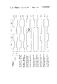
- FIG. 1 is a block diagram of a system according to this invention
- FIG. 2 shows time diagrams concerning the operation of the system shown in FIG. 1.
- FIG. 1 relates to an incoming time-division switch in an exchange. Basically it comprises a speech memory I, a time-division addressing memory 2 associated with memory 1, an input circuit 3 which receives samples from incoming trunk lines J connected to the switch and updating circuit 4 which insures synchronization of incoming samples with clock 6 of the exchange. the exchange control unit 5 and finally circuits of the insertion device according to this invention.
- memory 1 is the element which makes possible the time-division switching, assuming that memory 1 comprises n rows, each row capable of storing a sample and receiving at each cycle of N elementary time N samples in a predetermined order.
- memory I can transmit those N samples in an order different than the reception order.
- input circuit 3 and updating circuit 4- constitutes a switching interface are the circuits which make possible the insertion of speech samples into speech memory 1.
- Time-division addressing memory 2 makes it possible to transfer samples in a selected order provided that those various circuits are controlled as far as those operations are concerned by exchange control unit 5.
- each elementary time is divided in two portions (or half elementary times), one portion being assigned to write operations in memory I and the other portion being assigned to read operations in memory 1. In this way, write and read operations are interlaced.
- Circuit 3 nonnally provides speech sample at each of the N elementary times of the above mentioned cycle, samples for a time-division channel being transmitted at elementary times of same rank during successive cycles.
- Updating circuit 4 provides an address for each speech sample outgoing from circuit 3. That address is employed for insertion of a sample into a specific row of speech memory 1. Every sample from a time-division 3 channel is sequentially inserted into the same row in speech memory 1.
- Time-division'addressing memory 2 causes, atthe right time, the transfer of each sample stored in speech memory 1. For that purpose time-division memory 2 receives from unit for each newly established communication the time-division address at which the sample must be read from'speech memory 1 and an indication of the time at which that address must be transmitted to memory 1, such a time indication corresponding to the address at which the time division address is stored in memory 2.
- Insertion of samples into circuit 3 is not controlled by control unit of the local exchange but by a remote exchange from which the considered samples are received. As a result. it is normally not possible to insert data into rows of the speech memory 1 if they have not been inserted in the remote exchange. However, during traffic the'channels are not'continuously utilized which permits insertion of data into corresponding rows which are not utilized in speech memory 1. Eventually, even if every row is utilized, the frequencies utilized in known time-division switching networks are such that deletion of a speech sample from time to time during a communication is possible, since it has no effect on intellegibility of the corresponding communication. However, this cannot be considered in the case of data transmission.
- the present invention permits the elimination of a sample from time to time and insertion instead of sample control data.
- control data it appears of interest to insert control data at the switching network input. However, it may be desired to insert control data at a switching network output in order to possibly control the transmission network which follows the switching network.
- incoming time-division switch data inputs of speech memory 1 are connected to write control means connected between them, control unit 5 and input circuit 3.
- Those write control means are basically made of AND-OR units comprising an OR circuit 7 having as many outputs as data inputs in speech memory 1, and control AND circuits 8 and 10.
- the OR circuit 7 may be supplied, on the one hand, from circuit 3 via buffer register 24 and control circuit 8 and, on the other hand, by marker 9 via control circuit 10.
- Marker 9 is a circuit connected between computer assembly 11 of control unit 5 and the different circuits of the'time-division switch which may receive orders from'asse'mbly l1 and transmit to it information concerning their operation.
- addressing inputs of memory 1 are connected to addressing control means connected between them, control unit 5 and updating circuit 4.
- Addressing control means comprise read addressing means which are conventional and basically constituted' by time-division address memory 2. They also comprise write addressing which combine an arrangement according to this invention with a conventional arrangement.
- OR circuit 12 provides access to addressing input of memory 1. 1n read operation it is selectively supplied from memory 2, via control AND circuit 13 and, in write operation it is controlled by updating circuit 4, via buffer register 22 and control AND circuit or by marker 9, via control AND circuit 14.
- a control memory 16 is provided in order to solve the above mentioned access aproblems.
- Memory 16 has as many cells as rows in memory 1 so that each cell in memory 16 is associated to each row in memory 1 and makes possible a write operation and a read operation per elementary time in the same manner as in memory 1.
- Memory 16 is supplied and controlled in write operation by marker 9, via AND circuit 18 and OR circuit 17 while it is controlled in read operation by input circuit 4, via AND circuit 21 and OR circuit 17.
- Output of memory 16 is connected to AND circuits 8, 10, 14 and 15, via register 19, to control write operations into speech memory 1 and makes it possible to insert control data into a selected row of speech memory 1 at times which are normally utilized for writing speech samples.
- Forcible register 19 may be preset so as to make possible insertion of control data at successive elementary times, to enable systematic tests, or for completely isolating the switching interface circuits 3 and 4 in case of failure of one of those circuits.
- updating circuit 4 provides an address for writing into the speech memory 1 a sample supplied during the same elementary time from input circuit 3, as shown in diagram 20. That address is simultaneously transmitted to AND circuit 15 of the memory 1 for the write operation and to AND circuit 21 of the control memory 16 for the read operation. Since memory 16 must provide information either authorizing or refusing normal addressing and transfer of the sample transmitted from circuit 3 and that address simultaneously arrives at AND circuits 15 and 21, register 19'must supply that information during and preferably before the duration of half elementary time during which writing of the considered sample is possible as shown in time diagram 2f.
- any address provided from switching interface 4 appears during the half elementary time corresponding to the read operation for the speech memory 1 and the control memory 16 which eliminates any previous erroneous writing into memory 1 due to read inhibition existing in the absence of a suitable signal delivered from clock 6.
- Reversely address delivered from circuit 4 must continue during the complete half elementary time if the corresponding sample is to be written into speech memory 1, that addressbeing then without influence on AND circuit 21 due to the read inhibition existing in the absence of a suitable signal delivered from clock 6.
- Timing registers 22 and 24 are provided for insuring the presence of addresses and samples during the desired time.
- That information is transmitted to AND circuit 8 and via inverters and 23, so as to authorize normal writing of sample from input circuit 3 at the address de livered from switching interface 4 during half elementary time following the occurrence of the address from interface 4 as shown in time diagrams 2g and 21' 1.
- the half time is allotted to write into speech memory 1 and control memory 16 due to clock 6 operating AND circuits l4, l5 and 18, circuit 14 being inhibited by signal 0 applied to one of its input.
- marker 9 may write a control information 1 into any one of the cells of control memory 16 at an address which it provides according to selection predetermined by exchange maintenance people for control purposes.
- the sample stored in speech memory 1 during the previously considered half time is then read in a usual manner at the selected elementary time, this operation being conventionally controlled by time-division addressing memory 2 as shown in time diagram 2j.
- a cell of memory 16 contains information 1
- readout of that information during the half time results in the transmission of that information to register 19 during the same half time.
- that information is transmitted to AND circuits l0 and 14 and operates those circuits while it is transmitted in an inverted form to AND circuits 8 and 15 and renders those circuits inoperative as shown in time diagrams 2/1 and 2i in FIG. 2.
- marker 9 provides in response to exchange maintenance people wishes control data equivalent to a sample and the address at which those data must be stored in speech memory 1 provided that the delivered address is selected among those of samples which may be deleted that not among samples to be transmitted.
- Data are transmitted via AND circuit 10 and data addresses are transmitted via AND circuit 14. Those must be provided during the write half-time.
- Read-out of those data is controlled by time-division addressing memory 2 as read-out of the content of any other row in speech memory 1 as shown in time diagram 2j.
- register 19 may be directly set-up so that it continuously delivers information of logic value 1 so as to make possible insertion of control data into successive memory rows according to the hereabove described process which as mentioned also enables the deletion of any sample from the switching interface, if necessary.
- a system for inserting control data into the speech memory of a time-division switch comprising a speech memory.
- write addressing means coupled responsive to the condition of the memory element of the store means associated with a speech memory row to authorize the addressing of that memory row when the associated element is in a first condition and to substitute the selected addressing of another row for the addressing of that row when the associated memory element is in a second condition
- speech memory write control means responsive to the condition of the memory element associated with a speech memory row to authorize insertion of the expected speech sample into that row when the memory element associated with that row is in a first condition and to substitute data for the expected sample when the memory element associated with that row is in a second condition.
- the store means are basically constituted by a control memory incorporating as many cells as there are rows in the associated speech memory, and means connecting the read addressing input of the control memory to the circuit which delivers write addresses to the speech memory in parallel with a read addressing input of the speech memory, the write input and write addressing inputs of the said control memory being supplied from the switching network control unit.
- the invention as claimed in claim 2 including a forcible register connected between the control memory output and the control input, the said forcible register being settable by the control unit to a condition corresponding to the second condition of the memory element so as to make it possible to write control data into one or more rows of the speech memory during a cycle.
Abstract
A system is disclosed for enabling control data to be inserted into a speech memory of a time division switching system in place of speech samples. The control data may then be used for maintenance and test purposes. In the system, a control memory is provided with cells associated with a speech memory row which normally stores a speech sample. Depending upon the condition of the appropriate control memory cells, either the speech sample or the control data is inserted into the speech memory row. Control circuits provide appropriate switching signals during half-time of the TDM elementary time.
Description
United States Patent 1191 Lager et al.
[ Nov. 18, 1975 DATA INSERTION IN THE SPEECH 3.828.136 8/1974 Perna 179/15 BF ME OF A TIME DIVISION 3,860.761 l/l975 ONeill 179/15 BY SWITCHING SYSTEM [75] Inventors: Jean-Paul Lager, La-Celle-St-Cloud; Primary Examiner-Ralph D. Blakeslee Didier Refol, Boulogne-Billancourt, Attorney, Agent, or Firm-James B. Raden; Delbert P. both of France Warner [73] Assignee: International Standard Electric Corporation, New York, N.Y. 22 Filed: Sept. 16, 1974 [57] ABSTRACT [21] App]. No.: 506,420 A system is disclosed for enabling control data to be inserted into a speech memory of a time division switching system in place of speech samples. The con- [30] Forelgn Apphcatlon Pnonty Data trol data may then be used for maintenance and test Sept. I8, 1973 France purposes In the ystem a control memory is provided with cells associated with a speech memory row which [52] 179/15 BY; 179/15 AF; 179/15 BF normally stores a speech sample. Depending upon the [51] Int. CL- H04J 3/12 condition f h appropriate c tr l memory cells, ei-
[58] held of Search 179/15 15 AT, 15 A0, ther the speech sample or the control data is inserted 179/15 BY, 15 BF into the speech memory row. Control circuits provide appropriate switching signals during half-time of the References Clted TDM elementary time.
UNITED STATES PATENTS 3,748,393 7/1973 Baxter: 179/15 AF 5 Claims, 2 Drawing Figures COMPUTER 'NPUT ASSEMBLY mm 3 l 'gl C l) I\l T lR H 6 g R 71mm;
UNIT v I h REGISTERS I 1 oc1 I R L I aras ,INVERTER Ml id/ 8 10 AND AND 0R INVERTER TIME DIVISION SPEECH ADDRESSING MEMORY MEMORY REGISTER Sheet 1 0f 2 US. Patent Nov. 18, 1975 DATA INSERTION IN THE SPEECH MEMORY OF A TIME DIVISION SWITCHING SYSTEM BACKGROUND OF THE INVENTION 1. Field of the Invention The present invention relates to a system for inserting control data into a speech memory in a time-division switch.
2. Description of the Prior Art In a conventional time division multiplex switching system data received in the speech memory consists only of speech samples which are sequentially received sample by sample at different elementary times. The content of those speech samples is independent of the data to the control unit which controls the switching network comprising the considered time-division switch. From the viewpoint of the supervision of communications and testing of time-division switch network operation, the possibility of inserting known control data into a speech memory is of interest so that control data may be transmitted through the switching network as if speech samples only were being passed. Comparison of control data before and after transfer makes it possible to control the continuity of paths concerning newly established communications and to detect failures in the switching network. As communication established and failure may occur at any time, controls must be operated at all times without disturbing communications transiting through the switching network.
A known device enables the insertion of data instead of speech samples into a speech memory. For that purpose a comparator is utilized wherein the address of the sample to be replaced by data is displayed. When that address is delivered from the switching interface which supplies the considered speech memory the sample is blocked and the selected data are substituted therefore. A drawback of that device is low flexibility, since normal write addressing of a row must necessarily be delayed to make data insertion possible.
In addition with the foregoing system, a comparator serves only one row at a time and as many comparators as involved rows are therefore necessary if it is desired to insert data into several rows at a time. Then it will be preferable to have the possibility to address every speech memory row by a simple operation, particularly since such a possibility would enable the system to switch off the switching interface which supplies samples to the speech memory when that interface has failed.
SUMMARY OF THE INVENTION For purposes of the present invention there is provided a device for inserting control data into a speech memory during the normal operation of the time-division switch including the speech memory. The insertion is made possible at any write time into any one of the speech memory rows, even though all the rows are filled with control data during a cycle. The insertion is done in such a way as to permit efficient control of the continuity of a newly established path and to enable the system to detect switching network failures. All this is done without disturbing the established communications transiting through the network.
According to a feature of this invention, the device includes store means permitting the association of an individual memory element with each speech memory row. The device also comprises write addressing control means responsive to 'the condition of the memory element associated with a speech memory row so as to authorize the addressing of that memory row when the associated element is in a first condition and to substitute the selected addressing of any row of the addressing of that row when the associated memory element is in a second condition. Still the device comprises speech memory write control means which are responsive to the condition of the memory element associated with a speech memory row so as to authorize insertion of the foreseen speech sample into that row when the memory element associated with that row is in a first condition and to substitute data for the foreseen speech sample when the memory element associated with that row is in a second condition.
BRIEF DESCRIPTION OF THE DRAWINGS Other features of the present invention will appear more clearly from the following description of an embodiment, the said description being made in conjunction with accompanying drawings, wherein:
FIG. 1 is a block diagram of a system according to this invention,
FIG. 2 shows time diagrams concerning the operation of the system shown in FIG. 1.
DESCRIPTION OF A PREFERRED EMBODIMENT FIG. 1 relates to an incoming time-division switch in an exchange. Basically it comprises a speech memory I, a time-division addressing memory 2 associated with memory 1, an input circuit 3 which receives samples from incoming trunk lines J connected to the switch and updating circuit 4 which insures synchronization of incoming samples with clock 6 of the exchange. the exchange control unit 5 and finally circuits of the insertion device according to this invention.
In a known manner memory 1 is the element which makes possible the time-division switching, assuming that memory 1 comprises n rows, each row capable of storing a sample and receiving at each cycle of N elementary time N samples in a predetermined order. In addition, memory I can transmit those N samples in an order different than the reception order.
As shown in FIG. 1, input circuit 3 and updating circuit 4- constitutes a switching interface are the circuits which make possible the insertion of speech samples into speech memory 1. Time-division addressing memory 2 makes it possible to transfer samples in a selected order provided that those various circuits are controlled as far as those operations are concerned by exchange control unit 5.
In a conventional manner, each elementary time is divided in two portions (or half elementary times), one portion being assigned to write operations in memory I and the other portion being assigned to read operations in memory 1. In this way, write and read operations are interlaced.
Circuit 3 nonnally provides speech sample at each of the N elementary times of the above mentioned cycle, samples for a time-division channel being transmitted at elementary times of same rank during successive cycles.
Updating circuit 4 provides an address for each speech sample outgoing from circuit 3. That address is employed for insertion of a sample into a specific row of speech memory 1. Every sample from a time-division 3 channel is sequentially inserted into the same row in speech memory 1. Time-division'addressing memory 2 causes, atthe right time, the transfer of each sample stored in speech memory 1. For that purpose time-division memory 2 receives from unit for each newly established communication the time-division address at which the sample must be read from'speech memory 1 and an indication of the time at which that address must be transmitted to memory 1, such a time indication corresponding to the address at which the time division address is stored in memory 2.
Insertion of samples into circuit 3 is not controlled by control unit of the local exchange but by a remote exchange from which the considered samples are received. As a result. it is normally not possible to insert data into rows of the speech memory 1 if they have not been inserted in the remote exchange. However, during traffic the'channels are not'continuously utilized which permits insertion of data into corresponding rows which are not utilized in speech memory 1. Eventually, even if every row is utilized, the frequencies utilized in known time-division switching networks are such that deletion of a speech sample from time to time during a communication is possible, since it has no effect on intellegibility of the corresponding communication. However, this cannot be considered in the case of data transmission.
Therefore; if there is a'need', the present invention permits the elimination of a sample from time to time and insertion instead of sample control data. However, it is generally preferable to use free time-division channels, that is free rows in the speech memory 1.
To the extent that switching network control is more particularly involved, it appears of interest to insert control data at the switching network input. However, it may be desired to insert control data at a switching network output in order to possibly control the transmission network which follows the switching network.
By way of example, in the case of incoming time-division switch data, inputs of speech memory 1 are connected to write control means connected between them, control unit 5 and input circuit 3. Those write control means are basically made of AND-OR units comprising an OR circuit 7 having as many outputs as data inputs in speech memory 1, and control AND circuits 8 and 10. The OR circuit 7 may be supplied, on the one hand, from circuit 3 via buffer register 24 and control circuit 8 and, on the other hand, by marker 9 via control circuit 10. Marker 9 is a circuit connected between computer assembly 11 of control unit 5 and the different circuits of the'time-division switch which may receive orders from'asse'mbly l1 and transmit to it information concerning their operation.
Also for that purpose addressing inputs of memory 1 are connected to addressing control means connected between them, control unit 5 and updating circuit 4. Addressing control means comprise read addressing means which are conventional and basically constituted' by time-division address memory 2. They also comprise write addressing which combine an arrangement according to this invention with a conventional arrangement. OR circuit 12 provides access to addressing input of memory 1. 1n read operation it is selectively supplied from memory 2, via control AND circuit 13 and, in write operation it is controlled by updating circuit 4, via buffer register 22 and control AND circuit or by marker 9, via control AND circuit 14.
Obviously AND circuits 8 and 10 on the one hand, and AND circuits 1 4 and 15, on the other hand, must not be simultaneously operative,'AND circuits l0 and 14 being operative only in case of control data insertion. According to this invention, a control memory 16 is provided in order to solve the above mentioned access aproblems. Memory 16 has as many cells as rows in memory 1 so that each cell in memory 16 is associated to each row in memory 1 and makes possible a write operation and a read operation per elementary time in the same manner as in memory 1. Memory 16 is supplied and controlled in write operation by marker 9, via AND circuit 18 and OR circuit 17 while it is controlled in read operation by input circuit 4, via AND circuit 21 and OR circuit 17.
Output of memory 16 is connected to AND circuits 8, 10, 14 and 15, via register 19, to control write operations into speech memory 1 and makes it possible to insert control data into a selected row of speech memory 1 at times which are normally utilized for writing speech samples.
During operation of the system according to this invention conventional interlacing of write and read operations is maintained for speech memory 1 and utilized for control memory 16 as shown in time diagrams 2a, 2b, 2c and 2d.
At each elementary time, via register 22, updating circuit 4 provides an address for writing into the speech memory 1 a sample supplied during the same elementary time from input circuit 3, as shown in diagram 20. That address is simultaneously transmitted to AND circuit 15 of the memory 1 for the write operation and to AND circuit 21 of the control memory 16 for the read operation. Since memory 16 must provide information either authorizing or refusing normal addressing and transfer of the sample transmitted from circuit 3 and that address simultaneously arrives at AND circuits 15 and 21, register 19'must supply that information during and preferably before the duration of half elementary time during which writing of the considered sample is possible as shown in time diagram 2f. To make possible previous addressing of control memory 16, any address provided from switching interface 4 appears during the half elementary time corresponding to the read operation for the speech memory 1 and the control memory 16 which eliminates any previous erroneous writing into memory 1 due to read inhibition existing in the absence of a suitable signal delivered from clock 6.
Reversely address delivered from circuit 4 must continue during the complete half elementary time if the corresponding sample is to be written into speech memory 1, that addressbeing then without influence on AND circuit 21 due to the read inhibition existing in the absence of a suitable signal delivered from clock 6. Timing registers 22 and 24 are provided for insuring the presence of addresses and samples during the desired time.
Any address received by AND circuit 21 during the half elementary time in read operation of control memory 16, such halftime being determined by clock 6 and controlled by signal 11 from circuit 21 is transmitted to OR circuit 17 and results in the reading of the corresponding cell from memory 16. Normally that cell contains logic information 0 which is transmitted to register 19 during the half elementary time corresponding to the read operation for control memory 16.
That information is transmitted to AND circuit 8 and via inverters and 23, so as to authorize normal writing of sample from input circuit 3 at the address de livered from switching interface 4 during half elementary time following the occurrence of the address from interface 4 as shown in time diagrams 2g and 21' 1. The half time is allotted to write into speech memory 1 and control memory 16 due to clock 6 operating AND circuits l4, l5 and 18, circuit 14 being inhibited by signal 0 applied to one of its input. Simultaneously, marker 9 may write a control information 1 into any one of the cells of control memory 16 at an address which it provides according to selection predetermined by exchange maintenance people for control purposes.
The sample stored in speech memory 1 during the previously considered half time is then read in a usual manner at the selected elementary time, this operation being conventionally controlled by time-division addressing memory 2 as shown in time diagram 2j.
If a cell of memory 16 contains information 1, readout of that information during the half time results in the transmission of that information to register 19 during the same half time. During the following write half time, that information is transmitted to AND circuits l0 and 14 and operates those circuits while it is transmitted in an inverted form to AND circuits 8 and 15 and renders those circuits inoperative as shown in time diagrams 2/1 and 2i in FIG. 2.
Addressing and transferring a sample input circuit 3 are forbidden which results in the loss of such a sample. On the contrary, marker 9 provides in response to exchange maintenance people wishes control data equivalent to a sample and the address at which those data must be stored in speech memory 1 provided that the delivered address is selected among those of samples which may be deleted that not among samples to be transmitted.
Data are transmitted via AND circuit 10 and data addresses are transmitted via AND circuit 14. Those must be provided during the write half-time.
Read-out of those data is controlled by time-division addressing memory 2 as read-out of the content of any other row in speech memory 1 as shown in time diagram 2j.
In case of systematic trials or tests concerning a large number of speech memory rows, register 19 may be directly set-up so that it continuously delivers information of logic value 1 so as to make possible insertion of control data into successive memory rows according to the hereabove described process which as mentioned also enables the deletion of any sample from the switching interface, if necessary.
While the principles of the present invention have hereabove been described in relation to a specific embodimcnt. it will be clearly understood that the said description has only been made by way of example and does not limit the scope of the invention.
What is claimed is:
l. A system for inserting control data into the speech memory of a time-division switch comprising a speech memory.
a switching network control unit.
store means enabling the association of an individual memory element of the store means with each row in the speech memory,
write addressing means coupled responsive to the condition of the memory element of the store means associated with a speech memory row to authorize the addressing of that memory row when the associated element is in a first condition and to substitute the selected addressing of another row for the addressing of that row when the associated memory element is in a second condition,
speech memory write control means responsive to the condition of the memory element associated with a speech memory row to authorize insertion of the expected speech sample into that row when the memory element associated with that row is in a first condition and to substitute data for the expected sample when the memory element associated with that row is in a second condition.
2. The invention according to claim 1, in which the store means are basically constituted by a control memory incorporating as many cells as there are rows in the associated speech memory, and means connecting the read addressing input of the control memory to the circuit which delivers write addresses to the speech memory in parallel with a read addressing input of the speech memory, the write input and write addressing inputs of the said control memory being supplied from the switching network control unit.
3. The invention as claimed in claim 2, including a forcible register connected between the control memory output and the control input, the said forcible register being settable by the control unit to a condition corresponding to the second condition of the memory element so as to make it possible to write control data into one or more rows of the speech memory during a cycle.
4. The invention as claimed in claim 3, in which the write addressing control means are connected between said forcible register, the output of the circuit delivering write addresses to speech memory and the switching network control unit so as to transmit an address to the said speech memory at each elementary time.
5. The invention as claimed in claim 3 in which the memory write control means is connected between the forcible register, the output of the circuit delivering speech samples to speech memory and switching network control unit.
Claims (5)
1. A system for inserting control data into the speech memory of a time-division switch comprising a speech memory, a switching network control unit, store means enabling the association of an individual memory element of the store means with each row in the speech memory, write addressing means coupled responsive to the condition of the memory element of the store means associated with a speech memory row to authorize the addressing of that memory row when the associated element is in a first condition and to substitute the selected addressing of another row for the addressing of that row when the associated memory element is in a second condition, speech memory write control means responsive to the condition of the memory element associated with a speech memory row to authorize insertion of the expected speech sample into that row when the memory element associated with that row is in a first condition and to substitute data for the expected sample when the memory element associated with that row is in a second condition.
2. The invention according to claim 1, in which the store means are basically constituted by a control memory incorporating as many cells as there are rows in the associated speech memory, and means connecting the read addressing input of the control memory to the circuit which delivers write addresses to the speech memory in parallel with a read addressing input of the speech memory, the write input and write addressing inputs of the said control memory being supplied from the switching network control unit.
3. The invention as claimed in claim 2, including a forcible register connected between the control memory output and the control input, the said forcible register being settable by the control unit to a condition corresponding to the second condition of the memory element so as to make it possible to write control data into one or more rows of the speech memory during a cycle.
4. The invention as claimed in claim 3, in which the write addressing control means are connected between said forcible register, the output of the circuIt delivering write addresses to speech memory and the switching network control unit so as to transmit an address to the said speech memory at each elementary time.
5. The invention as claimed in claim 3 in which the memory write control means is connected between the forcible register, the output of the circuit delivering speech samples to speech memory and switching network control unit.
Applications Claiming Priority (1)
| Application Number | Priority Date | Filing Date | Title |
|---|---|---|---|
| FR7333395A FR2248758A5 (en) | 1973-09-18 | 1973-09-18 |
Publications (1)
| Publication Number | Publication Date |
|---|---|
| US3920920A true US3920920A (en) | 1975-11-18 |
Family
ID=9125179
Family Applications (1)
| Application Number | Title | Priority Date | Filing Date |
|---|---|---|---|
| US506420A Expired - Lifetime US3920920A (en) | 1973-09-18 | 1974-09-16 | Data insertion in the speech memory of a time division switching system |
Country Status (6)
| Country | Link |
|---|---|
| US (1) | US3920920A (en) |
| BE (1) | BE820037A (en) |
| CH (1) | CH589398A5 (en) |
| DE (1) | DE2442673C2 (en) |
| FR (1) | FR2248758A5 (en) |
| GB (1) | GB1466433A (en) |
Cited By (4)
| Publication number | Priority date | Publication date | Assignee | Title |
|---|---|---|---|---|
| US4059729A (en) * | 1976-06-09 | 1977-11-22 | Martin Marietta Aerospace | Method and system for selectively accessing multiplexed data transmission network for monitoring and testing of the network |
| FR2532505A1 (en) * | 1982-08-30 | 1984-03-02 | Western Electric Co | MAINTENANCE OF SWITCHING SYSTEMS COMMANDED BY A MEMORIZED PROGRAM |
| US4698802A (en) * | 1986-03-07 | 1987-10-06 | American Telephone And Telegraph Company And At&T Information Systems Inc. | Combined circuit and packet switching system |
| US5347566A (en) * | 1991-10-23 | 1994-09-13 | Digital Transmission Systems, Inc. | Retrofit subscriber loop carrier system with improved performance monitoring and remote provisioning |
Families Citing this family (3)
| Publication number | Priority date | Publication date | Assignee | Title |
|---|---|---|---|---|
| US4298977A (en) * | 1979-09-10 | 1981-11-03 | Bell Telephone Laboratories, Incorporated | Broadcast and alternate message time slot interchanger |
| US4296492A (en) * | 1979-12-26 | 1981-10-20 | Bell Telephone Laboratories, Incorporated | Continuity verification arrangement |
| GB2083319B (en) * | 1980-06-25 | 1984-03-28 | Plessey Co Ltd | Digital switching module |
Citations (3)
| Publication number | Priority date | Publication date | Assignee | Title |
|---|---|---|---|---|
| US3748393A (en) * | 1970-02-17 | 1973-07-24 | Int Standard Electric Corp | Data transmission over pulse code modulation channels |
| US3828136A (en) * | 1971-06-18 | 1974-08-06 | Sits Soc It Telecom Siemens | Time division telephone switching exchange |
| US3860761A (en) * | 1973-06-14 | 1975-01-14 | Bell Telephone Labor Inc | Digital progressively controlled switching system |
-
1973
- 1973-09-18 FR FR7333395A patent/FR2248758A5/fr not_active Expired
-
1974
- 1974-09-06 DE DE2442673A patent/DE2442673C2/en not_active Expired
- 1974-09-12 GB GB3979074A patent/GB1466433A/en not_active Expired
- 1974-09-16 US US506420A patent/US3920920A/en not_active Expired - Lifetime
- 1974-09-17 CH CH1263174A patent/CH589398A5/xx not_active IP Right Cessation
- 1974-09-18 BE BE2053867A patent/BE820037A/en unknown
Patent Citations (3)
| Publication number | Priority date | Publication date | Assignee | Title |
|---|---|---|---|---|
| US3748393A (en) * | 1970-02-17 | 1973-07-24 | Int Standard Electric Corp | Data transmission over pulse code modulation channels |
| US3828136A (en) * | 1971-06-18 | 1974-08-06 | Sits Soc It Telecom Siemens | Time division telephone switching exchange |
| US3860761A (en) * | 1973-06-14 | 1975-01-14 | Bell Telephone Labor Inc | Digital progressively controlled switching system |
Cited By (5)
| Publication number | Priority date | Publication date | Assignee | Title |
|---|---|---|---|---|
| US4059729A (en) * | 1976-06-09 | 1977-11-22 | Martin Marietta Aerospace | Method and system for selectively accessing multiplexed data transmission network for monitoring and testing of the network |
| FR2532505A1 (en) * | 1982-08-30 | 1984-03-02 | Western Electric Co | MAINTENANCE OF SWITCHING SYSTEMS COMMANDED BY A MEMORIZED PROGRAM |
| US4493073A (en) * | 1982-08-30 | 1985-01-08 | At&T Bell Laboratories | Maintenance of stored program controlled switching systems |
| US4698802A (en) * | 1986-03-07 | 1987-10-06 | American Telephone And Telegraph Company And At&T Information Systems Inc. | Combined circuit and packet switching system |
| US5347566A (en) * | 1991-10-23 | 1994-09-13 | Digital Transmission Systems, Inc. | Retrofit subscriber loop carrier system with improved performance monitoring and remote provisioning |
Also Published As
| Publication number | Publication date |
|---|---|
| FR2248758A5 (en) | 1975-05-16 |
| AU7323574A (en) | 1976-03-18 |
| DE2442673C2 (en) | 1984-03-29 |
| BE820037A (en) | 1975-03-18 |
| CH589398A5 (en) | 1977-06-30 |
| DE2442673A1 (en) | 1975-03-27 |
| GB1466433A (en) | 1977-03-09 |
Similar Documents
| Publication | Publication Date | Title |
|---|---|---|
| US3458659A (en) | Nonblocking pulse code modulation system having storage and gating means with common control | |
| US5202885A (en) | Atm exchange with copying capability | |
| US4488290A (en) | Distributed digital exchange with improved switching system and input processor | |
| US4569043A (en) | Arrangement for interfacing the space stage to the time stages of a T-S-T digital switching system | |
| US4935922A (en) | Packet data switch for transferring data packets from one or a plurality of incoming data links to one or a plurality of outgoing data links | |
| KR920010220B1 (en) | Time division switching system control arrangement and method | |
| CA1274304A (en) | Crosspoint circuitry for data packet space division switches | |
| US3963870A (en) | Time-division multiplex switching system | |
| US4608684A (en) | Digital switching systems employing multi-channel frame association apparatus | |
| KR960700599A (en) | Data Transfer Switch, Access Control Asynchronous Transfer Mode (ATM) Switch, and Controlled Information Cell Flow Control Method (Controlled Access ATM Switch) | |
| US5014268A (en) | Parallel time slot interchanger matrix and switch block module for use therewith | |
| JPH07105813B2 (en) | Distributed packet switching system | |
| US4345325A (en) | Message-interchange circuitry for microprocessors linked by synchronous communication network | |
| US5805590A (en) | Switching device for digital data networks and asynchronous transfer mode | |
| EP0114822B1 (en) | Communication arrangements for distributed control systems | |
| US3920920A (en) | Data insertion in the speech memory of a time division switching system | |
| GB1454827A (en) | Fault detection process and system for time-division switching network | |
| EP0039948B1 (en) | Pcm switching element | |
| US3909562A (en) | Switching network testing process and arrangement | |
| US3989894A (en) | Synchronism error detecting and correcting system for a circulating memory | |
| GB1470701A (en) | Digital switching system | |
| JPH0217743A (en) | Exchange module | |
| JPH04287494A (en) | Time-division switch and connection module composing such switch | |
| CA1061883A (en) | Data insertion in the speech memory of a time division switching system | |
| CA1127766A (en) | Time division switching circuit with time slot interchange |
Legal Events
| Date | Code | Title | Description |
|---|---|---|---|
| AS | Assignment |
Owner name: ALCATEL N.V., DE LAIRESSESTRAAT 153, 1075 HK AMSTE Free format text: ASSIGNMENT OF ASSIGNORS INTEREST.;ASSIGNOR:INTERNATIONAL STANDARD ELECTRIC CORPORATION, A CORP OF DE;REEL/FRAME:004718/0023 Effective date: 19870311 |