US4377794A - Charge transfer device comb filter with improved frequency response - Google Patents

Charge transfer device comb filter with improved frequency response Download PDF

Info

Publication number
US4377794A
US4377794A US06/240,922 US24092281A US4377794A US 4377794 A US4377794 A US 4377794A US 24092281 A US24092281 A US 24092281A US 4377794 A US4377794 A US 4377794A
Authority
US
United States
Prior art keywords
delay line
ccd
transfer
long
short
Prior art date
Legal status (The legal status is an assumption and is not a legal conclusion. Google has not performed a legal analysis and makes no representation as to the accuracy of the status listed.)
Expired - Fee Related
Application number
US06/240,922
Inventor
Tatsuo Sakaue
Chikara Sato
Current Assignee (The listed assignees may be inaccurate. Google has not performed a legal analysis and makes no representation or warranty as to the accuracy of the list.)
Toshiba Corp
Original Assignee
Tokyo Shibaura Electric Co Ltd
Priority date (The priority date is an assumption and is not a legal conclusion. Google has not performed a legal analysis and makes no representation as to the accuracy of the date listed.)
Filing date
Publication date
Application filed by Tokyo Shibaura Electric Co Ltd filed Critical Tokyo Shibaura Electric Co Ltd
Assigned to TOKYO SHIBAURA DENKI KABUSHIKI KAISHA reassignment TOKYO SHIBAURA DENKI KABUSHIKI KAISHA ASSIGNMENT OF ASSIGNORS INTEREST. Assignors: SAKAUE TATSUO, SATO CHIKARA
Application granted granted Critical
Publication of US4377794A publication Critical patent/US4377794A/en
Anticipated expiration legal-status Critical
Expired - Fee Related legal-status Critical Current

Links

Images

Classifications

    • HELECTRICITY
    • H03ELECTRONIC CIRCUITRY
    • H03HIMPEDANCE NETWORKS, e.g. RESONANT CIRCUITS; RESONATORS
    • H03H15/00Transversal filters
    • H03H15/02Transversal filters using analogue shift registers

Definitions

  • This invention relates to a charge coupled device (CCD) comb filter.
  • Comb filters can be used as a means for separating a luminance video signal Y and a chrominance video signal C included in a colorplexed composite video signal, and as a ground echo canceller for radar signals.
  • a comb filter for use in separating the luminance video signal and chrominance video signal uses a 1-H delay line for delaying a colorplexed composite video signal by one-horizontal total line period H (63.5 ⁇ s).
  • a delayed composite video signal and undelayed composite video signal are additively combined to obtain the luminance signal Y and the delayed composite video signal and undelayed composite video signal are subtractively combined to obtain the chrominance video signal C.
  • a glass delay line is used as the 1-H delay line, but it has disadvantages in that it would be difficult to obtain an accurate delay time and that the delay time varies with temperature.
  • a comb filter using a CCD delay line capable of providing an accurate 1-H delay time is disclosed by D. J. Sauer et al in a paper entitled “A CCD Comb Filter IC for TV Receivers", 1980 IEE International Solid-State Circuits Conference, Digest of Technical papers page 32, Feb. 13, 1980.
  • Such a CCD comb filter is shown in FIG. 1.
  • a colorplexed composite video signal applied to an input terminal 10 is supplied to a long CCD delay line 11, to a first short CCD delay line 12 and through an inverting amplifier 14 with a gain of unity to a second short CCD delay line 13 having the number of stages equal to that of the CCD delay line 12.
  • a charge signal from the long CCD delay line 11 is combined with a charge signal from the short CCD delay line 12 to provide a luminance video signal Y.
  • the charge signal from the long CCD delay line 11 is combined with a charge signal from the short CCD delay line 13 to provide a chrominance signal C.
  • a delay time Td provided by the long CCD delay line 11 is defined as follows:
  • N 2 the number of stages of the long CCD delay line 11
  • N 1 the number of stages of the short CCD delay lines 12 and 13
  • ⁇ of the short delay line is equal to ⁇ of the long delay line and the number of stages of the short delay lines is 1 or so, then N 1 ⁇ N 2 ⁇ .
  • a variation in the gain characteristic and delay time characteristic of the short delay line due to the transfer inefficiency ⁇ can be neglected.
  • f ADJ is set at the color subcarrier frequency f SC of 3.58 MHz.
  • Equation (4) From Equation (4) the gain characteristic
  • Another object of this invention is to provide, in order to improve the comb filter characteristics, a CCD comb filter having long and short CCD delay lines connected to receive a common input signal, in which the length of transfer electrodes of the short CCD delay line as viewed in charge transfer direction is made longer than that of transfer electrodes of the long CCD delay line.
  • a CCD comb filter including long and short CCD delay lines connected to receive a common input signal and arranged to combine an output charge packet of the long CCD delay line with that of the short CCD delay line
  • the product of the number of stages of the long CCD delay line and transfer inefficiency of each stage thereof is set substantially equal to that of the number of stages of the short CCD delay line and transfer inefficiency of each stage thereof.
  • the length of transfer electrodes of the short CCD delay line as viewed in the charge transfer direction is formed larger than that of transfer electrodes of the long CCD delay line.
  • FIG. 1 shows a schematic arrangement of a CCD comb filter
  • FIG. 2 shows the frequency response of the long CCD delay line and short CCD delay line
  • FIG. 3 shows an arrangement for explaining a CCD comb filter of this invention.
  • FIGS. 4 and 5 each, show a schematic arrangement of long and short CCD delay lines of the comb filter of FIG. 3.
  • a CCD comb filter embodying this invention like the comb filter as shown in FIG. 1, comprises a long CCD delay line 21, first and second short CCD delay lines 22 and 23, first and second CCD output lines 25 and 26 and an inverting amplifier 24 having a gain of unity.
  • the long CCD delay line 21 has N 2 stages each having a transfer inefficiency ⁇ 2 and the first and second short CCD delay lines 22 and 23 have N 1 stages each having a transfer inefficiency ⁇ 1 .
  • the first and second CCD output lines 25, 26 include N 3 stages each having a transfer inefficiency ⁇ 3 .
  • the comb filter of this invention is so designed that the number of stages N 1 and N 2 of the delay lines and transfer inefficiencies ⁇ 1 and ⁇ 2 have the following relation:
  • the transfer function of the comb filter is found as follows:
  • Equations (13) and (14) are the same as those of an ideal comb filter. According to this invention, a comb filter very close to the ideal comb filter can be realized, using a charge transfer device having a finite transfer inefficiency.
  • the transfer inefficiency is produced due to a variety of reasons. In any case, all of the charge packet is not transferred from stage to stage in a finite time. That is, this is due to the fact that the transfer speed of the charge packet is slow.
  • the transfer speed of the charge packet is dependent upon the thermal diffusion, self-induced drift, fringing field drift, etc., particularly upon the thermal diffusion.
  • the time constant of thermal diffusion can be expressed as follows:
  • L length of a transfer electrode as viewed in charge transfer direction
  • FIGS. 4 and 5 each, diagrammatically show an arrangement of CCD delay lines which may be used as the long delay line 21 and short delay lines 22, 23 as shown in FIG. 3.
  • the CCD delay lines as shown in FIGS. 4 and 5 use a potential equilibration method to inject charges and two-phase driving system.
  • a predetermined amount of charge is injected into a semiconductor substrate 31 by a source region 32 formed in the substrate which is supplied with a source pulse ⁇ s-1 .
  • An input signal V in is applied to an input electrode 33 adjacent to the source region so that a charge packet corresponding to an instantaneous amplitude of the input signal is transferred to a potential well below a gate electrode 34 to which a predetermined voltage V G is applied and temporarily stored therein.
  • a sampling pulse ⁇ SP is applied to a sampling electrode 35, the charge packet stored below the gate electrode 34 is transferred to the region below a transfer electrode 36.
  • the charge packet is transferred under the action of clock pulses ⁇ 1 and ⁇ 2 along a channel which is formed below transfer electrodes 36, 37, . . . , 44.
  • the transfer electrodes 35, 36, 37 and 38 form a first stage N 2 of the long CCD line 21 as shown in FIG. 3 and the transfer electrodes 39, 40, 41 and 42 form the second stage N 2-1 .
  • the short CCD delay line of FIG. 5 has an arrangement similar to the long CCD delay line of FIG. 4.
  • a charge is injected through a source region 52 in the substrate 31.
  • the injected charge is modulated by an input signal V in which is applied to an input electrode 53, with the result that a charge packet corresponding to an instantaneous amplitude of the input signal V in is transferred to a potential well below a gate electrode 54 to which an adjusting voltage V ADJ is applied.
  • the charge packet stored below the gate electrode 54 is transferred by a sampling electrode 55, to which the sampling pulse ⁇ SP is applied, to a channel below transfer electrodes 56, 57, 58, 59, 60 . . . .
  • the sampling pulse ⁇ SP is applied
  • the gate electrode 54 supplied with the adjusting voltage V ADJ is adapted to cause a charge packet the same in quantity as that injected into the long delay line of FIG. 4 to be injected into the short delay line when a common input signal V in is applied to an input terminal.
  • the electrodes 55 to 58 form the first stage N 1 of the short delay line.
  • the length of the transfer electrodes of the short CCD delay line as viewed in the charge transfer direction is set longer than that of the transfer electrodes of the long CCD delay line.
  • the above-mentioned comb depth D and the error ⁇ f of the actual null frequency with respect to the theoretic null frequency (3.58 MHz) are
  • the electrode length corresponding to ⁇ 2 is 10 microns, the electrode length corresponding to ⁇ 1 will be about 70 microns.

Landscapes

  • Processing Of Color Television Signals (AREA)
  • Filters That Use Time-Delay Elements (AREA)

Abstract

A CCD comb filter includes long and short CCD delay lines connected to receive a common input signal and is arranged to combine output signals of the long and short CCD delay lines. In order to realize a CCD comb filter very close to an optimum comb filter the product of the number of stages of the long CCD delay line and the transfer inefficiency of each stage thereof is set substantially equal to the product of the number of stages of the short CCD delay line and the transfer inefficiency of each stage thereof. In order that the transfer inefficiency of the short CCD delay line may be made greater to satisfy the above-mentioned requirement, transfer electrodes of the short CCD delay line are designed such that their length as viewed in charge transfer direction is made larger than the length of transfer electrodes of the long CCD delay line.

Description

This invention relates to a charge coupled device (CCD) comb filter.
Comb filters can be used as a means for separating a luminance video signal Y and a chrominance video signal C included in a colorplexed composite video signal, and as a ground echo canceller for radar signals.
A comb filter for use in separating the luminance video signal and chrominance video signal uses a 1-H delay line for delaying a colorplexed composite video signal by one-horizontal total line period H (63.5 μs). A delayed composite video signal and undelayed composite video signal are additively combined to obtain the luminance signal Y and the delayed composite video signal and undelayed composite video signal are subtractively combined to obtain the chrominance video signal C.
In the past, a glass delay line is used as the 1-H delay line, but it has disadvantages in that it would be difficult to obtain an accurate delay time and that the delay time varies with temperature.
A comb filter using a CCD delay line capable of providing an accurate 1-H delay time is disclosed by D. J. Sauer et al in a paper entitled "A CCD Comb Filter IC for TV Receivers", 1980 IEE International Solid-State Circuits Conference, Digest of Technical papers page 32, Feb. 13, 1980. Such a CCD comb filter is shown in FIG. 1.
In the CCD comb filter shown in FIG. 1, a colorplexed composite video signal applied to an input terminal 10 is supplied to a long CCD delay line 11, to a first short CCD delay line 12 and through an inverting amplifier 14 with a gain of unity to a second short CCD delay line 13 having the number of stages equal to that of the CCD delay line 12. At a CCD channel 15 a charge signal from the long CCD delay line 11 is combined with a charge signal from the short CCD delay line 12 to provide a luminance video signal Y. At a CCD channel 16, on the other hand, the charge signal from the long CCD delay line 11 is combined with a charge signal from the short CCD delay line 13 to provide a chrominance signal C.
A delay time Td provided by the long CCD delay line 11 is defined as follows:
Td=(N.sub.2 -N.sub.1)/f.sub.c                              ( 1)
where
N2 =the number of stages of the long CCD delay line 11
N1 =the number of stages of the short CCD delay lines 12 and 13
fc =transfer clock pulse frequency
Now suppose that N1 =1, N2 =683.5 and fc =10.7 MHz. Then, Td=63.5 μs. From this it will appreciated that an accurate 1-H delay time can be provided in spite of the circumferential conditions.
Since in the charge transfer device, however, a transfer inefficiency defined as a residual amount of charge packet per stage is normally finite (of the order of 10-3 to 10-5), the gain characteristic R(f) and delay time characteristic Td(f) of the comb filter are different from ideal ones. As conveniently known in the art, these characteristics can be expressed as follows: ##EQU1##
If, in the above-mentioned comb filter, ε of the short delay line is equal to ε of the long delay line and the number of stages of the short delay lines is 1 or so, then N1 ε<<N2 ε. A variation in the gain characteristic and delay time characteristic of the short delay line due to the transfer inefficiency ε can be neglected.
Therefore, the transfer function relating to the luminance signal Y of the comb filter of FIG. 1 can be expressed as follows, by referring to FIG. 2. ##EQU2## where z-1 = cos 2πfTd-j sin 2πfTd and fADJ denotes an adjusting frequency at which the gain of the long CCD delay line is equal to that of the short CCD delay line. In order to obtain the luminance signal Y, fADJ is set at the color subcarrier frequency fSC of 3.58 MHz.
From Equation (4) the gain characteristic |H(f)| and phase characteristic Q(f) of the comb filter are found as follows: ##EQU3## where Td denotes a delay time as expressed in Equation (3).
Suppose, for example, that N=N2 -N1 =682.5, ε=1×10⁻⁴, fADJ≃ fSC =3.579545 MHz and fc =3fSC =10.7 MHz. From Equation (5) the comb depth at f=fSC, that is, at a theoretic null frequency, can be calculated as follows: ##EQU4## A difference between the actual null frequency and theoretic null frequency is ##EQU5##
Where, therefore, ε is finite, the degradation of comb characteristic occurs. Where the actual null frequency is deviated from the theoretic null frequency, a separation between the luminance signal and chrominance signal is lowered.
It is accordingly an object of this invention to provide a CCD comb filter having an improved comb filter characteristic.
Another object of this invention is to provide, in order to improve the comb filter characteristics, a CCD comb filter having long and short CCD delay lines connected to receive a common input signal, in which the length of transfer electrodes of the short CCD delay line as viewed in charge transfer direction is made longer than that of transfer electrodes of the long CCD delay line.
In accordance with this invention, in a CCD comb filter including long and short CCD delay lines connected to receive a common input signal and arranged to combine an output charge packet of the long CCD delay line with that of the short CCD delay line, the product of the number of stages of the long CCD delay line and transfer inefficiency of each stage thereof is set substantially equal to that of the number of stages of the short CCD delay line and transfer inefficiency of each stage thereof.
In order to make the transfer inefficiency of the short CCD delay line greater than the transfer inefficiency of the long CCD delay line the length of transfer electrodes of the short CCD delay line as viewed in the charge transfer direction is formed larger than that of transfer electrodes of the long CCD delay line.
This invention can be more fully understood from the following detailed description when taken in conjunction with the accompanying drawings, in which:
FIG. 1 shows a schematic arrangement of a CCD comb filter;
FIG. 2 shows the frequency response of the long CCD delay line and short CCD delay line;
FIG. 3 shows an arrangement for explaining a CCD comb filter of this invention; and
FIGS. 4 and 5, each, show a schematic arrangement of long and short CCD delay lines of the comb filter of FIG. 3.
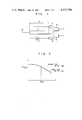
Referring to FIG. 3 a CCD comb filter embodying this invention, like the comb filter as shown in FIG. 1, comprises a long CCD delay line 21, first and second short CCD delay lines 22 and 23, first and second CCD output lines 25 and 26 and an inverting amplifier 24 having a gain of unity. As shown in FIG. 3, the long CCD delay line 21 has N2 stages each having a transfer inefficiency ε2 and the first and second short CCD delay lines 22 and 23 have N1 stages each having a transfer inefficiency ε1. The first and second CCD output lines 25, 26 include N3 stages each having a transfer inefficiency ε3.
The comb filter of this invention is so designed that the number of stages N1 and N2 of the delay lines and transfer inefficiencies ε1 and ε2 have the following relation:
N.sub.1 ε.sub.1 ≃N.sub.2 ε.sub.2
In the comb filter of FIG. 3 the gain characteristic R1 (f) and delay time characteristic Td1 (f) of the short delay lines 22, 23 and gain characteristic R2 (f) and delay time characteristic Td(f) of the long delay line 21 are given below ##EQU6##
The transfer function of the comb filter is found as follows:
H(z)=R.sub.1 (f)z.sub.1.sup.-1 +R.sub.2 (f)z.sub.2.sup.-1  (12)
where
z.sub.1.sup.-1 = cos 2πfTd.sub.1 -j sin 2πfTd.sub.1
z.sub.2.sup.-1 = cos 2πfTd.sub.2 -j sin 2πfTd.sub.2
If N1 ε1 ≃N2 ε2, the gain response and phase response are given by
|H(f)|=2| cos πfTd.sub.0 |(13)
θ(f)=-πfTd.sub.0                                  (14) ##EQU7##
The gain response and phase response of Equations (13) and (14) are the same as those of an ideal comb filter. According to this invention, a comb filter very close to the ideal comb filter can be realized, using a charge transfer device having a finite transfer inefficiency.
In the charge transfer device, the transfer inefficiency is produced due to a variety of reasons. In any case, all of the charge packet is not transferred from stage to stage in a finite time. That is, this is due to the fact that the transfer speed of the charge packet is slow. The transfer speed of the charge packet is dependent upon the thermal diffusion, self-induced drift, fringing field drift, etc., particularly upon the thermal diffusion.
The time constant of thermal diffusion can be expressed as follows:
τth=4L.sup.2 /π.sup.2 D.sup.2                       (15)
where
D=diffusion coefficient (constant) of carriers
L=length of a transfer electrode as viewed in charge transfer direction
From Equation (15) it will be appreciated that the larger the transfer electrode as viewed in charge transfer direction the greater the time constant of thermal diffusion i.e. the lower the charge transfer speed becomes and hence the charge transfer speed or the transfer inefficiency can be adjusted by the length of the transfer electrode.
FIGS. 4 and 5, each, diagrammatically show an arrangement of CCD delay lines which may be used as the long delay line 21 and short delay lines 22, 23 as shown in FIG. 3. The CCD delay lines as shown in FIGS. 4 and 5 use a potential equilibration method to inject charges and two-phase driving system.
In the long CCD delay line as shown in FIG. 4, a predetermined amount of charge is injected into a semiconductor substrate 31 by a source region 32 formed in the substrate which is supplied with a source pulse φs-1. An input signal Vin is applied to an input electrode 33 adjacent to the source region so that a charge packet corresponding to an instantaneous amplitude of the input signal is transferred to a potential well below a gate electrode 34 to which a predetermined voltage VG is applied and temporarily stored therein. When a sampling pulse φSP is applied to a sampling electrode 35, the charge packet stored below the gate electrode 34 is transferred to the region below a transfer electrode 36. Thereafter, the charge packet is transferred under the action of clock pulses φ1 and φ2 along a channel which is formed below transfer electrodes 36, 37, . . . , 44. In FIG. 4, the transfer electrodes 35, 36, 37 and 38 form a first stage N2 of the long CCD line 21 as shown in FIG. 3 and the transfer electrodes 39, 40, 41 and 42 form the second stage N2-1.
The short CCD delay line of FIG. 5 has an arrangement similar to the long CCD delay line of FIG. 4. A charge is injected through a source region 52 in the substrate 31. The injected charge is modulated by an input signal Vin which is applied to an input electrode 53, with the result that a charge packet corresponding to an instantaneous amplitude of the input signal Vin is transferred to a potential well below a gate electrode 54 to which an adjusting voltage VADJ is applied. The charge packet stored below the gate electrode 54 is transferred by a sampling electrode 55, to which the sampling pulse φSP is applied, to a channel below transfer electrodes 56, 57, 58, 59, 60 . . . . In the arrangement as shown in FIG. 5, the gate electrode 54 supplied with the adjusting voltage VADJ is adapted to cause a charge packet the same in quantity as that injected into the long delay line of FIG. 4 to be injected into the short delay line when a common input signal Vin is applied to an input terminal. The electrodes 55 to 58 form the first stage N1 of the short delay line.
In order to achieve N1 ε1 ≃N2 ε2, as shown in FIGS. 4 and 5, the length of the transfer electrodes of the short CCD delay line as viewed in the charge transfer direction is set longer than that of the transfer electrodes of the long CCD delay line. In this case, it is not necessarily required that N1 ε1 =N2 ε2. An error is allowed within a range of ±50%. Suppose, for example, that ε2 =5×10⁻³ when N1 =692.5, ε1 =1×10⁻⁴ and N2 =10. In this case, the above-mentioned comb depth D and the error Δf of the actual null frequency with respect to the theoretic null frequency (3.58 MHz) are
D=42 dB
Δf=42 Hz
These values are in a practically allowable range. If under the above-mentioned conditions the electrode length corresponding to ε2 is 10 microns, the electrode length corresponding to ε1 will be about 70 microns.

Claims (2)

What we claim is:
1. A CCD comb filter including long and short CCD delay lines connected to receive a common input signal and arranged to combine output charge packets of said long and short CCD delay lines characterized in that the product of the number of stages of said long CCD delay line and transfer inefficiency of each stage thereof is substantially equal to that of the number of stages of said short CCD delay line and transfer inefficiency of each stage thereof.
2. A CCD comb filter including long and short CCD delay lines connected to receive a common input signal and each having transfer electrodes driven by a common clock pulse to transfer signal charge packets, output charge packets of said long and short CCD delay lines being combined, characterized in that the length of transfer electrodes of said short CCD delay line as viewed in the charge transfer direction is larger than that of said transfer electrodes of said long CCD delay line.
US06/240,922 1980-03-18 1981-03-05 Charge transfer device comb filter with improved frequency response Expired - Fee Related US4377794A (en)

Applications Claiming Priority (2)

Application Number Priority Date Filing Date Title
JP3335080A JPS56131278A (en) 1980-03-18 1980-03-18 Charge transfer type comb-shaped filter
JP55-33350 1980-03-18

Publications (1)

Publication Number Publication Date
US4377794A true US4377794A (en) 1983-03-22

Family

ID=12384119

Family Applications (1)

Application Number Title Priority Date Filing Date
US06/240,922 Expired - Fee Related US4377794A (en) 1980-03-18 1981-03-05 Charge transfer device comb filter with improved frequency response

Country Status (3)

Country Link
US (1) US4377794A (en)
JP (1) JPS56131278A (en)
GB (1) GB2073523B (en)

Cited By (4)

* Cited by examiner, † Cited by third party
Publication number Priority date Publication date Assignee Title
US4510522A (en) * 1982-05-28 1985-04-09 Rca Corporation CCD Comb filter employing floating gate subtractor techniques
US4554858A (en) * 1982-08-13 1985-11-26 Nippon Gakki Seizo Kabushiki Kaisha Digital filter for an electronic musical instrument
DE3605759A1 (en) * 1985-03-19 1986-09-25 N.V. Philips' Gloeilampenfabrieken, Eindhoven COLOR TV RECEIVER WITH A TELEVISION CIRCUIT FOR CONVERTING A TIME MULTIPLEX SIGNAL INTO SIMULTANEOUS SIGNALS AND SUITABLE INTEGRATED CIRCUIT ARRANGEMENT
US5705836A (en) * 1995-05-22 1998-01-06 Dalsa, Inc. Efficient charge transfer structure in large pitch charge coupled device

Families Citing this family (1)

* Cited by examiner, † Cited by third party
Publication number Priority date Publication date Assignee Title
NL8204727A (en) * 1982-12-07 1984-07-02 Philips Nv CARGO TRANSFER.

Non-Patent Citations (1)

* Cited by examiner, † Cited by third party
Title
D. J. Sauer et al., A CCD Comb Filter IC for TV Receivers, 1980 IEEE International Solid-State Circuits Conference, p. 32, (Feb. 13, 1980). *

Cited By (4)

* Cited by examiner, † Cited by third party
Publication number Priority date Publication date Assignee Title
US4510522A (en) * 1982-05-28 1985-04-09 Rca Corporation CCD Comb filter employing floating gate subtractor techniques
US4554858A (en) * 1982-08-13 1985-11-26 Nippon Gakki Seizo Kabushiki Kaisha Digital filter for an electronic musical instrument
DE3605759A1 (en) * 1985-03-19 1986-09-25 N.V. Philips' Gloeilampenfabrieken, Eindhoven COLOR TV RECEIVER WITH A TELEVISION CIRCUIT FOR CONVERTING A TIME MULTIPLEX SIGNAL INTO SIMULTANEOUS SIGNALS AND SUITABLE INTEGRATED CIRCUIT ARRANGEMENT
US5705836A (en) * 1995-05-22 1998-01-06 Dalsa, Inc. Efficient charge transfer structure in large pitch charge coupled device

Also Published As

Publication number Publication date
GB2073523B (en) 1984-03-28
JPS56131278A (en) 1981-10-14
GB2073523A (en) 1981-10-14

Similar Documents

Publication Publication Date Title
US4096516A (en) Electronic signal processing apparatus
US4220977A (en) Signal transmission circuit
US4205335A (en) Circuit arrangement for separating chrominance and luminance information in a composite video signal of an NTSC system
US4281339A (en) Color solid state image pick-up apparatus
US4053932A (en) Ghost signal eliminating system
US4044381A (en) Automatic waveform equalizing system for television receiver
US4377794A (en) Charge transfer device comb filter with improved frequency response
US4217605A (en) Comb filter employing a charge transfer device with plural mutually proportioned signal charge inputs
US4628347A (en) Charge transfer device for multiplexing signals
US4509181A (en) CCD charge substraction arrangement
US4325076A (en) Electronic filter for generating a third harmonic signal
US3843930A (en) Time delay controller circuit for reducing time jitter between signal groups
US4510522A (en) CCD Comb filter employing floating gate subtractor techniques
US4387389A (en) Semiconductor filter using charge transfer device
US4255676A (en) Semiconductor phase shift device for a charge transfer filter
US4454534A (en) Method and apparatus for filtering the luminance signal from ACCVS television signal
DE2341852A1 (en) MULTIPLEX DEMODULATOR FOR A COLOR TV SIGNAL
DE2754511C3 (en) PAL decoder for processing a color carrier frequency PAL chrominance signal
JPS6250005B2 (en)
KR830000669B1 (en) Comb filter
Tanigawa et al. A multipurpose CCD comb filter with combing and delaying functions
US4249201A (en) Color decoder for color television receiver
KR820001556B1 (en) Electronic signal processing apparatus
Tanigawa et al. Rejection characteristics in a video-signal processor using CCD comb filters
JPS6232558B2 (en)

Legal Events

Date Code Title Description
AS Assignment

Owner name: TOKYO SHIBAURA DENKI KABUSHIKI KAISHA, 72 HORIKAWA

Free format text: ASSIGNMENT OF ASSIGNORS INTEREST.;ASSIGNORS:SAKAUE TATSUO;SATO CHIKARA;REEL/FRAME:003871/0897

Effective date: 19810223

FEPP Fee payment procedure

Free format text: PAYOR NUMBER ASSIGNED (ORIGINAL EVENT CODE: ASPN); ENTITY STATUS OF PATENT OWNER: LARGE ENTITY

MAFP Maintenance fee payment

Free format text: PAYMENT OF MAINTENANCE FEE, 4TH YEAR, PL 96-517 (ORIGINAL EVENT CODE: M170); ENTITY STATUS OF PATENT OWNER: LARGE ENTITY

Year of fee payment: 4

FEPP Fee payment procedure

Free format text: MAINTENANCE FEE REMINDER MAILED (ORIGINAL EVENT CODE: REM.); ENTITY STATUS OF PATENT OWNER: LARGE ENTITY

LAPS Lapse for failure to pay maintenance fees
STCH Information on status: patent discontinuation

Free format text: PATENT EXPIRED DUE TO NONPAYMENT OF MAINTENANCE FEES UNDER 37 CFR 1.362

FP Lapsed due to failure to pay maintenance fee

Effective date: 19910324