US4361720A - Low thermal resistance insulating support and base or box for power component incorporating such a support - Google Patents
Low thermal resistance insulating support and base or box for power component incorporating such a support Download PDFInfo
- Publication number
- US4361720A US4361720A US06/145,023 US14502380A US4361720A US 4361720 A US4361720 A US 4361720A US 14502380 A US14502380 A US 14502380A US 4361720 A US4361720 A US 4361720A
- Authority
- US
- United States
- Prior art keywords
- support
- beryllium oxide
- support according
- metal member
- metal
- Prior art date
- Legal status (The legal status is an assumption and is not a legal conclusion. Google has not performed a legal analysis and makes no representation as to the accuracy of the status listed.)
- Expired - Lifetime
Links
- LTPBRCUWZOMYOC-UHFFFAOYSA-N beryllium oxide Inorganic materials O=[Be] LTPBRCUWZOMYOC-UHFFFAOYSA-N 0.000 claims abstract description 19
- FRWYFWZENXDZMU-UHFFFAOYSA-N 2-iodoquinoline Chemical compound C1=CC=CC2=NC(I)=CC=C21 FRWYFWZENXDZMU-UHFFFAOYSA-N 0.000 claims abstract description 15
- ZOKXTWBITQBERF-UHFFFAOYSA-N Molybdenum Chemical compound [Mo] ZOKXTWBITQBERF-UHFFFAOYSA-N 0.000 claims abstract description 5
- 239000011733 molybdenum Substances 0.000 claims abstract description 5
- 229910052750 molybdenum Inorganic materials 0.000 claims abstract description 4
- 229910052751 metal Inorganic materials 0.000 claims description 26
- 239000002184 metal Substances 0.000 claims description 26
- 238000000576 coating method Methods 0.000 claims description 12
- 239000004020 conductor Substances 0.000 claims description 5
- WFKWXMTUELFFGS-UHFFFAOYSA-N tungsten Chemical compound [W] WFKWXMTUELFFGS-UHFFFAOYSA-N 0.000 claims description 3
- 239000010937 tungsten Substances 0.000 claims description 3
- 229910001092 metal group alloy Inorganic materials 0.000 claims description 2
- 229910052721 tungsten Inorganic materials 0.000 claims description 2
- RTAQQCXQSZGOHL-UHFFFAOYSA-N Titanium Chemical compound [Ti] RTAQQCXQSZGOHL-UHFFFAOYSA-N 0.000 claims 2
- 239000010936 titanium Substances 0.000 claims 2
- 229910052719 titanium Inorganic materials 0.000 claims 2
- RYGMFSIKBFXOCR-UHFFFAOYSA-N Copper Chemical compound [Cu] RYGMFSIKBFXOCR-UHFFFAOYSA-N 0.000 abstract description 3
- 239000010949 copper Substances 0.000 abstract description 3
- 229910052802 copper Inorganic materials 0.000 abstract description 2
- 230000008646 thermal stress Effects 0.000 abstract 1
- 239000008188 pellet Substances 0.000 description 9
- 239000011248 coating agent Substances 0.000 description 7
- 238000005219 brazing Methods 0.000 description 5
- 229910001316 Ag alloy Inorganic materials 0.000 description 2
- 230000006835 compression Effects 0.000 description 2
- 238000007906 compression Methods 0.000 description 2
- 238000001816 cooling Methods 0.000 description 2
- 239000000463 material Substances 0.000 description 2
- 229910000679 solder Inorganic materials 0.000 description 2
- 229910000881 Cu alloy Inorganic materials 0.000 description 1
- 229910000846 In alloy Inorganic materials 0.000 description 1
- 229910001182 Mo alloy Inorganic materials 0.000 description 1
- 229910000978 Pb alloy Inorganic materials 0.000 description 1
- XUIMIQQOPSSXEZ-UHFFFAOYSA-N Silicon Chemical compound [Si] XUIMIQQOPSSXEZ-UHFFFAOYSA-N 0.000 description 1
- 229910001362 Ta alloys Inorganic materials 0.000 description 1
- 229910001080 W alloy Inorganic materials 0.000 description 1
- 229910045601 alloy Inorganic materials 0.000 description 1
- 239000000956 alloy Substances 0.000 description 1
- 229910052790 beryllium Inorganic materials 0.000 description 1
- ATBAMAFKBVZNFJ-UHFFFAOYSA-N beryllium atom Chemical compound [Be] ATBAMAFKBVZNFJ-UHFFFAOYSA-N 0.000 description 1
- 239000003989 dielectric material Substances 0.000 description 1
- 230000005611 electricity Effects 0.000 description 1
- PCHJSUWPFVWCPO-UHFFFAOYSA-N gold Chemical compound [Au] PCHJSUWPFVWCPO-UHFFFAOYSA-N 0.000 description 1
- 229910052737 gold Inorganic materials 0.000 description 1
- 239000010931 gold Substances 0.000 description 1
- 230000012447 hatching Effects 0.000 description 1
- APFVFJFRJDLVQX-UHFFFAOYSA-N indium atom Chemical compound [In] APFVFJFRJDLVQX-UHFFFAOYSA-N 0.000 description 1
- 230000004048 modification Effects 0.000 description 1
- 238000012986 modification Methods 0.000 description 1
- 230000002093 peripheral effect Effects 0.000 description 1
- 230000001681 protective effect Effects 0.000 description 1
- 230000000630 rising effect Effects 0.000 description 1
- 229910052710 silicon Inorganic materials 0.000 description 1
- 239000010703 silicon Substances 0.000 description 1
- 239000004332 silver Substances 0.000 description 1
- GUVRBAGPIYLISA-UHFFFAOYSA-N tantalum atom Chemical compound [Ta] GUVRBAGPIYLISA-UHFFFAOYSA-N 0.000 description 1
- 238000003466 welding Methods 0.000 description 1
Images
Classifications
-
- H—ELECTRICITY
- H01—ELECTRIC ELEMENTS
- H01L—SEMICONDUCTOR DEVICES NOT COVERED BY CLASS H10
- H01L23/00—Details of semiconductor or other solid state devices
- H01L23/34—Arrangements for cooling, heating, ventilating or temperature compensation ; Temperature sensing arrangements
- H01L23/36—Selection of materials, or shaping, to facilitate cooling or heating, e.g. heatsinks
- H01L23/373—Cooling facilitated by selection of materials for the device or materials for thermal expansion adaptation, e.g. carbon
- H01L23/3735—Laminates or multilayers, e.g. direct bond copper ceramic substrates
-
- C—CHEMISTRY; METALLURGY
- C04—CEMENTS; CONCRETE; ARTIFICIAL STONE; CERAMICS; REFRACTORIES
- C04B—LIME, MAGNESIA; SLAG; CEMENTS; COMPOSITIONS THEREOF, e.g. MORTARS, CONCRETE OR LIKE BUILDING MATERIALS; ARTIFICIAL STONE; CERAMICS; REFRACTORIES; TREATMENT OF NATURAL STONE
- C04B37/00—Joining burned ceramic articles with other burned ceramic articles or other articles by heating
- C04B37/02—Joining burned ceramic articles with other burned ceramic articles or other articles by heating with metallic articles
- C04B37/023—Joining burned ceramic articles with other burned ceramic articles or other articles by heating with metallic articles characterised by the interlayer used
- C04B37/026—Joining burned ceramic articles with other burned ceramic articles or other articles by heating with metallic articles characterised by the interlayer used consisting of metals or metal salts
-
- H—ELECTRICITY
- H01—ELECTRIC ELEMENTS
- H01L—SEMICONDUCTOR DEVICES NOT COVERED BY CLASS H10
- H01L23/00—Details of semiconductor or other solid state devices
- H01L23/12—Mountings, e.g. non-detachable insulating substrates
- H01L23/14—Mountings, e.g. non-detachable insulating substrates characterised by the material or its electrical properties
- H01L23/15—Ceramic or glass substrates
-
- C—CHEMISTRY; METALLURGY
- C04—CEMENTS; CONCRETE; ARTIFICIAL STONE; CERAMICS; REFRACTORIES
- C04B—LIME, MAGNESIA; SLAG; CEMENTS; COMPOSITIONS THEREOF, e.g. MORTARS, CONCRETE OR LIKE BUILDING MATERIALS; ARTIFICIAL STONE; CERAMICS; REFRACTORIES; TREATMENT OF NATURAL STONE
- C04B2237/00—Aspects relating to ceramic laminates or to joining of ceramic articles with other articles by heating
- C04B2237/02—Aspects relating to interlayers, e.g. used to join ceramic articles with other articles by heating
- C04B2237/12—Metallic interlayers
- C04B2237/122—Metallic interlayers based on refractory metals
-
- C—CHEMISTRY; METALLURGY
- C04—CEMENTS; CONCRETE; ARTIFICIAL STONE; CERAMICS; REFRACTORIES
- C04B—LIME, MAGNESIA; SLAG; CEMENTS; COMPOSITIONS THEREOF, e.g. MORTARS, CONCRETE OR LIKE BUILDING MATERIALS; ARTIFICIAL STONE; CERAMICS; REFRACTORIES; TREATMENT OF NATURAL STONE
- C04B2237/00—Aspects relating to ceramic laminates or to joining of ceramic articles with other articles by heating
- C04B2237/30—Composition of layers of ceramic laminates or of ceramic or metallic articles to be joined by heating, e.g. Si substrates
- C04B2237/32—Ceramic
- C04B2237/34—Oxidic
-
- C—CHEMISTRY; METALLURGY
- C04—CEMENTS; CONCRETE; ARTIFICIAL STONE; CERAMICS; REFRACTORIES
- C04B—LIME, MAGNESIA; SLAG; CEMENTS; COMPOSITIONS THEREOF, e.g. MORTARS, CONCRETE OR LIKE BUILDING MATERIALS; ARTIFICIAL STONE; CERAMICS; REFRACTORIES; TREATMENT OF NATURAL STONE
- C04B2237/00—Aspects relating to ceramic laminates or to joining of ceramic articles with other articles by heating
- C04B2237/30—Composition of layers of ceramic laminates or of ceramic or metallic articles to be joined by heating, e.g. Si substrates
- C04B2237/40—Metallic
- C04B2237/407—Copper
-
- C—CHEMISTRY; METALLURGY
- C04—CEMENTS; CONCRETE; ARTIFICIAL STONE; CERAMICS; REFRACTORIES
- C04B—LIME, MAGNESIA; SLAG; CEMENTS; COMPOSITIONS THEREOF, e.g. MORTARS, CONCRETE OR LIKE BUILDING MATERIALS; ARTIFICIAL STONE; CERAMICS; REFRACTORIES; TREATMENT OF NATURAL STONE
- C04B2237/00—Aspects relating to ceramic laminates or to joining of ceramic articles with other articles by heating
- C04B2237/50—Processing aspects relating to ceramic laminates or to the joining of ceramic articles with other articles by heating
- C04B2237/64—Forming laminates or joined articles comprising grooves or cuts
-
- H—ELECTRICITY
- H01—ELECTRIC ELEMENTS
- H01L—SEMICONDUCTOR DEVICES NOT COVERED BY CLASS H10
- H01L2924/00—Indexing scheme for arrangements or methods for connecting or disconnecting semiconductor or solid-state bodies as covered by H01L24/00
- H01L2924/0001—Technical content checked by a classifier
- H01L2924/0002—Not covered by any one of groups H01L24/00, H01L24/00 and H01L2224/00
-
- H—ELECTRICITY
- H01—ELECTRIC ELEMENTS
- H01L—SEMICONDUCTOR DEVICES NOT COVERED BY CLASS H10
- H01L2924/00—Indexing scheme for arrangements or methods for connecting or disconnecting semiconductor or solid-state bodies as covered by H01L24/00
- H01L2924/30—Technical effects
- H01L2924/35—Mechanical effects
- H01L2924/351—Thermal stress
- H01L2924/3511—Warping
-
- Y—GENERAL TAGGING OF NEW TECHNOLOGICAL DEVELOPMENTS; GENERAL TAGGING OF CROSS-SECTIONAL TECHNOLOGIES SPANNING OVER SEVERAL SECTIONS OF THE IPC; TECHNICAL SUBJECTS COVERED BY FORMER USPC CROSS-REFERENCE ART COLLECTIONS [XRACs] AND DIGESTS
- Y10—TECHNICAL SUBJECTS COVERED BY FORMER USPC
- Y10T—TECHNICAL SUBJECTS COVERED BY FORMER US CLASSIFICATION
- Y10T403/00—Joints and connections
- Y10T403/21—Utilizing thermal characteristic, e.g., expansion or contraction, etc.
- Y10T403/217—Members having different coefficients of expansion
Definitions
- the invention relates to a low thermal resistance insulating support, which can more particularly be used for a power component such as a diode or a high frequency transistor.
- a power component such as a diode or a high frequency transistor.
- the bases or boxes incorporating such a support form part of the invention.
- a large amount of heat is produced in a small volume.
- a dissipative support (the base) is used and is made from a metal which is a good conductor of heat and electricity, which is itself in contact with air or a cooling device.
- connections of the component must be very large compared with the dimensions of the semiconducting pellet or pellets constituting the active part of the component.
- These connections are not then directly connected to the pellet or pellets and instead are welded to metal coatings deposited on an electrically insulating and thermally conductive intermediate support, which is indispensible for electrically insulating from at least part of the connections, while still permitting the removal of the heat.
- Beryllium oxide supplies a dielectric material whose thermal conductivity (0.6 cal.s -1 cm -1 ) which is almost as good as that of gold (0.7 cal.s -1 cm -1 ) and whose linear expansion coefficient (7.7. 10 -6 ) is matched to that of the silicon (7.6. 10 -6 ), so that the pellet can be directly welded to the beryllium oxide metal coating.
- the object of the invention is to eliminate the risks of BeO flaws, while still permitting high temperature brazing due to the compression of the metal of the base between the BeO and a disk made from an appropriate metal.
- the support according to the invention is of the type including a first element made from an electrically insulating and thermally conductive material welded to a second metal element with a higher expansion coefficient than that of the said material.
- the invention is characterised by the fact that the second element is such that one large face thereof opposite to the face welded to the first element and parallel to the latter is itself welded to a metal member (molybdenum, tungsten, tantalum or metal alloy) whose linear expansion coefficient is equal to or lower than that of the material.
- a metal member mobdenum, tungsten, tantalum or metal alloy
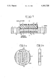
- FIG. 1 is a diagrammatic sectional view of an embodiment of the invention
- FIG. 2a is a plan view and FIG. 2b is a profile view of part of the device of FIG. 1.
- a copper base 1 has a central portion with a rounded shape, which substantially revolves about an axis XX and has two lugs with cylindrical holes of axes 10.
- base 1 is made thinner by two recesses 11 and 12, whose presence is not indispensible in the general case of the invention, so as to form a predetermined remaining thickiness t 1 therebetween.
- a beryllium oxide disk 2 is welded by a brazing disk 5 in the circular recess 11.
- a tungsten or molybdenum disk 3 is welded in recess 12 by a brazing disk 6 and has a thickness t 3 whose order of magnitude is substantially equivalent to that of the predetermined remaining thickness t 1 as shown in FIG. 1.
- Disk 2 clearly emerges from recess 11 and has metal coatings 21, 22, etc. One of these metal coatings covers part of the upper face of the disk, as well as part of its edge (see b in FIG. 2).
- Disk 3 is flush with and does not project beyond the face of base 1 adjacent thereto.
- a circular release groove 111 is provided on the periphery of recess 11 and facilitates the compression of the central part of the base during a temperature rise through the action of the connecting forces between disks 2 and 3 and this part of base 1. Such prevents the hard solder from rising up onto the BeO disc 2.
- FIG 2a shows the metallized face of the beryllium oxide disk 2 and FIG. 2b shows the edge of the metallized disk (hatched portion).
- This metallized portion constitutes the earth return of metal coating 21, also represented by hatching on the plan view.
- the metal coating 21, 22 shown in an exemplified manner are appropriate for the fitting of a transistor having four identical pellets welded in pairs to the regions 220 of the widest metal coating.
- the same metal coating 22 includes in its peripheral portion a welding region for a wide connecting strip (not shown). This connection is for example that of the transistor collector in the case where the electrode is connected to the rear face of the pellet welded to the metal coating 22.
- the two other input and/or output electrodes of the transistor are connected by connecting wires to metal coatings 21 and 23.
- base 1 centre diameter 14 mm, centre thickness 1.6 mm
- disk 2 beryllium oxide: diameter 14 mm, thickness 1.6 mm
- disk 3 molybdenum: diameter 14 mm, thickness 0.5 mm.
- the device constituted by the assembled parts forms a base or a box.
- the actual box has a protective cover (not shown) covering the central portion, i.e. the pellets and the connecting wires which are particularly vulnerable.
Abstract
A low thermal resistance insulating support permitting thermal stresses in the base of a high power component incorporating a beryllium oxide element without fractures or flaws occurring. The support includes a dissipating support made from copper, whose two large faces are slotted to at least partly house a beryllium oxide disk which receives a component and its connections to the outside. Such also completely houses a molybdenum disk with an expansion coefficient close to that of the beryllium oxide.
Description
1. Field of the Invention
The invention relates to a low thermal resistance insulating support, which can more particularly be used for a power component such as a diode or a high frequency transistor. The bases or boxes incorporating such a support form part of the invention.
2. Description of the Prior Art
In an electronic component having a relatively high power dissipation (from a few Watts to a few hundred Watts or even higher) a large amount of heat is produced in a small volume. To remove the heat, a dissipative support (the base) is used and is made from a metal which is a good conductor of heat and electricity, which is itself in contact with air or a cooling device.
Moreover, at high frequency (from a few dozen to a few hundred megahertz or even higher) the connections of the component must be very large compared with the dimensions of the semiconducting pellet or pellets constituting the active part of the component. These connections are not then directly connected to the pellet or pellets and instead are welded to metal coatings deposited on an electrically insulating and thermally conductive intermediate support, which is indispensible for electrically insulating from at least part of the connections, while still permitting the removal of the heat.
Beryllium oxide supplies a dielectric material whose thermal conductivity (0.6 cal.s-1 cm-1) which is almost as good as that of gold (0.7 cal.s-1 cm-1) and whose linear expansion coefficient (7.7. 10-6) is matched to that of the silicon (7.6. 10-6), so that the pellet can be directly welded to the beryllium oxide metal coating.
However, a problem arises on increasing the power up to and beyond 100 Watts over an area of about 1 cm2. In order to improve heat removal, it has been attempted either to spread the semiconducting pellets over the metal conductive coating of the oxide so that the thermal cones intersect below the beryllium oxide, i.e. in the metal base or in cooling device, leading to large beryllium disks, or to reduce for an equivalent surface area the beryllium oxide thickness, which in the end leads to the same result.
In both cases, flaws occur in the beryllium oxide when using high temperature brazing with an alloy of silver and copper, which is the only reliable compatible alloy. On using low temperature brazing with so-called soft solders (alloy of lead, silver and indium) there are no BeO flaws, but the reliability is less satisfactory.
The object of the invention is to eliminate the risks of BeO flaws, while still permitting high temperature brazing due to the compression of the metal of the base between the BeO and a disk made from an appropriate metal.
The support according to the invention is of the type including a first element made from an electrically insulating and thermally conductive material welded to a second metal element with a higher expansion coefficient than that of the said material.
The invention is characterised by the fact that the second element is such that one large face thereof opposite to the face welded to the first element and parallel to the latter is itself welded to a metal member (molybdenum, tungsten, tantalum or metal alloy) whose linear expansion coefficient is equal to or lower than that of the material.
Various other objects, features and attendant advantages of the present invention will be more fully appreciated as the same becomes better understood from the following detailed description when considered with the accompanying drawings in which like reference characters designate like or corresponding parts through the several views and wherein:
FIG. 1 is a diagrammatic sectional view of an embodiment of the invention;
FIG. 2a is a plan view and FIG. 2b is a profile view of part of the device of FIG. 1.
In the embodiment of FIG. 1, a copper base 1 has a central portion with a rounded shape, which substantially revolves about an axis XX and has two lugs with cylindrical holes of axes 10.
In its central portion, base 1 is made thinner by two recesses 11 and 12, whose presence is not indispensible in the general case of the invention, so as to form a predetermined remaining thickiness t1 therebetween. A beryllium oxide disk 2 is welded by a brazing disk 5 in the circular recess 11. A tungsten or molybdenum disk 3 is welded in recess 12 by a brazing disk 6 and has a thickness t3 whose order of magnitude is substantially equivalent to that of the predetermined remaining thickness t1 as shown in FIG. 1. Disk 2 clearly emerges from recess 11 and has metal coatings 21, 22, etc. One of these metal coatings covers part of the upper face of the disk, as well as part of its edge (see b in FIG. 2). Disk 3 is flush with and does not project beyond the face of base 1 adjacent thereto.
A circular release groove 111 is provided on the periphery of recess 11 and facilitates the compression of the central part of the base during a temperature rise through the action of the connecting forces between disks 2 and 3 and this part of base 1. Such prevents the hard solder from rising up onto the BeO disc 2.
FIG 2a shows the metallized face of the beryllium oxide disk 2 and FIG. 2b shows the edge of the metallized disk (hatched portion). This metallized portion constitutes the earth return of metal coating 21, also represented by hatching on the plan view.
The metal coating 21, 22 shown in an exemplified manner are appropriate for the fitting of a transistor having four identical pellets welded in pairs to the regions 220 of the widest metal coating. The same metal coating 22 includes in its peripheral portion a welding region for a wide connecting strip (not shown). This connection is for example that of the transistor collector in the case where the electrode is connected to the rear face of the pellet welded to the metal coating 22.
The two other input and/or output electrodes of the transistor are connected by connecting wires to metal coatings 21 and 23.
In the case of a transistor with a total power of 250 Watts, the dimensions of the essential parts are as follows:
base 1: centre diameter 14 mm, centre thickness 1.6 mm
disk 2: beryllium oxide: diameter 14 mm, thickness 1.6 mm
disk 3: molybdenum: diameter 14 mm, thickness 0.5 mm.
The device constituted by the assembled parts forms a base or a box. The actual box has a protective cover (not shown) covering the central portion, i.e. the pellets and the connecting wires which are particularly vulnerable.
Obviously, numerous additional modifications and variations of the present invention are possible in light of the above teachings. It is therefore to be understood that within the scope of the appended claims, the invention may be practiced otherwise than as specifically described herein.
Claims (8)
1. A low thermal resistance insulating support comprising:
a first element made from an electrically insulating and thermally conducting material and having a first face portion;
a second element integrally connected to said first element at said first face portion and made from a metal with a higher expansion coefficient than that of said thermally conducting material of said first element;
said second element having a first and second recess formed therein, and having a predetermined remaining thickness therebetween, said first recess being adjacent to the first face portion of said first element; and
a metal member mounted in said second recess having an expansion coefficient close to that of said thermally conducting material, and having a thickness whose order of magnitude is substantially equivalent to said remaining thickness of said second element wherein said metal member is mounted within said second recess such that an outer surface portion thereof is flush with the surface of said second element.
2. A support according to claim 1, the first element comprising beryllium oxide and the metal member comprising molybdenum.
3. A support according to claim 1, the first element comprising beryllium oxide and said metal member comprising titanium.
4. A support according to claim 1, said metal member comprising a disk.
5. A support according to claim 1, the first element comprising beryllium oxide and the metal member comprising tungsten.
6. A support according to claim 1, the first element comprising beryllium oxide and said metal member comprising a metal alloy having an expansion coefficient equivalent to titanium.
7. A support according to claim 1, wherein said second element has a circular release groove provided therein on the periphery of said first recess of said second element.
8. A support according to claim 1, further comprising a plurality of metal coatings mounted on said first element.
Applications Claiming Priority (2)
| Application Number | Priority Date | Filing Date | Title |
|---|---|---|---|
| FR7911023A FR2455785A1 (en) | 1979-05-02 | 1979-05-02 | ELECTRICAL INSULATOR SUPPORT, WITH LOW THERMAL RESISTANCE, AND BASE OR HOUSING FOR POWER COMPONENT, INCLUDING SUCH SUPPORT |
| FR7911023 | 1979-05-02 |
Publications (1)
| Publication Number | Publication Date |
|---|---|
| US4361720A true US4361720A (en) | 1982-11-30 |
Family
ID=9224926
Family Applications (1)
| Application Number | Title | Priority Date | Filing Date |
|---|---|---|---|
| US06/145,023 Expired - Lifetime US4361720A (en) | 1979-05-02 | 1980-04-30 | Low thermal resistance insulating support and base or box for power component incorporating such a support |
Country Status (5)
| Country | Link |
|---|---|
| US (1) | US4361720A (en) |
| EP (1) | EP0018890B1 (en) |
| JP (1) | JPS55150261A (en) |
| DE (1) | DE3061321D1 (en) |
| FR (1) | FR2455785A1 (en) |
Cited By (15)
| Publication number | Priority date | Publication date | Assignee | Title |
|---|---|---|---|---|
| DE3315583A1 (en) * | 1983-04-29 | 1984-10-31 | Siemens AG, 1000 Berlin und 8000 München | AN ELECTRICAL COMPONENT-CARRYING, EASILY COOLABLE CIRCUIT MODULE |
| US4563541A (en) * | 1983-01-07 | 1986-01-07 | L.C.C.-C.I.C.E.-Compagnie Europeenne De Composants Electroniques | Package providing high heat dissipation, in particular for microelectronics |
| US4571611A (en) * | 1982-03-31 | 1986-02-18 | Fujitsu Limited | Semiconductor chip with a metal heat radiator |
| US4574162A (en) * | 1982-03-26 | 1986-03-04 | Kaufman Lance R | Compact circuit package with improved construction for clamping to enhance heat transfer |
| US4630096A (en) * | 1984-05-30 | 1986-12-16 | Motorola, Inc. | High density IC module assembly |
| US4719631A (en) * | 1986-01-10 | 1988-01-12 | The United States Of America As Represented By The Secretary Of The Air Force | Conductively cooled laser diode array pumped laser |
| US4788627A (en) * | 1986-06-06 | 1988-11-29 | Tektronix, Inc. | Heat sink device using composite metal alloy |
| US4887149A (en) * | 1986-07-17 | 1989-12-12 | Sgs Microelectronica S.P.A. | Semiconductor device mounted in a highly flexible, segmented package, provided with heat sink |
| DE4032035A1 (en) * | 1989-10-20 | 1991-04-25 | Hughes Aircraft Co | High current feedthrough package for microelectronic power circuits - with high thermal conductivity and large contact area feed-through for efficient heat dissipation |
| EP0435155A1 (en) * | 1989-12-29 | 1991-07-03 | Sumitomo Electric Industries, Ltd. | Radiating fin having improved life and thermal conductivity |
| US5886407A (en) * | 1993-04-14 | 1999-03-23 | Frank J. Polese | Heat-dissipating package for microcircuit devices |
| US5886269A (en) * | 1995-02-17 | 1999-03-23 | Nippon Tungsten Co., Ltd. | Substrate and heat sink for a semiconductor and method of manufacturing the same |
| EP0935286A1 (en) * | 1997-05-26 | 1999-08-11 | Sumitomo Electric Industries, Ltd. | Copper circuit junction substrate and method of producing the same |
| US5972737A (en) * | 1993-04-14 | 1999-10-26 | Frank J. Polese | Heat-dissipating package for microcircuit devices and process for manufacture |
| US8991680B1 (en) * | 2005-05-25 | 2015-03-31 | Alfred E. Mann Foundation For Scientific Research | Method of manufacture of an electrode array |
Families Citing this family (2)
| Publication number | Priority date | Publication date | Assignee | Title |
|---|---|---|---|---|
| CA1200326A (en) * | 1982-11-26 | 1986-02-04 | Franco N. Sechi | High-power dual-gate field-effect transistor |
| EP0746022B1 (en) * | 1995-05-30 | 1999-08-11 | Motorola, Inc. | Hybrid multi-chip module and method of fabricating |
Citations (1)
| Publication number | Priority date | Publication date | Assignee | Title |
|---|---|---|---|---|
| US4227036A (en) * | 1978-09-18 | 1980-10-07 | Microwave Semiconductor Corp. | Composite flanged ceramic package for electronic devices |
Family Cites Families (6)
| Publication number | Priority date | Publication date | Assignee | Title |
|---|---|---|---|---|
| GB873803A (en) * | 1959-05-29 | 1961-07-26 | Westinghouse Brake & Signal | Improvements in or relating to semi-conductor devices |
| GB903824A (en) * | 1959-11-12 | 1962-08-22 | Ass Elect Ind | Improvements in ceramic-to-metal seals |
| FR1372216A (en) * | 1962-10-15 | 1964-09-11 | Asea Ab | Semiconductor device |
| FR1376243A (en) * | 1963-12-04 | 1964-10-23 | Thomson Houston Comp Francaise | Improvements to metal-ceramic seals |
| US4042952A (en) * | 1976-06-09 | 1977-08-16 | Motorola, Inc. | R. F. power transistor device with controlled common lead inductance |
| JPS5550646A (en) * | 1978-10-06 | 1980-04-12 | Hitachi Ltd | Integrated circuit device |
-
1979
- 1979-05-02 FR FR7911023A patent/FR2455785A1/en active Granted
-
1980
- 1980-04-23 DE DE8080400549T patent/DE3061321D1/en not_active Expired
- 1980-04-23 EP EP80400549A patent/EP0018890B1/en not_active Expired
- 1980-04-30 JP JP5854380A patent/JPS55150261A/en active Pending
- 1980-04-30 US US06/145,023 patent/US4361720A/en not_active Expired - Lifetime
Patent Citations (1)
| Publication number | Priority date | Publication date | Assignee | Title |
|---|---|---|---|---|
| US4227036A (en) * | 1978-09-18 | 1980-10-07 | Microwave Semiconductor Corp. | Composite flanged ceramic package for electronic devices |
Cited By (16)
| Publication number | Priority date | Publication date | Assignee | Title |
|---|---|---|---|---|
| US4574162A (en) * | 1982-03-26 | 1986-03-04 | Kaufman Lance R | Compact circuit package with improved construction for clamping to enhance heat transfer |
| US4571611A (en) * | 1982-03-31 | 1986-02-18 | Fujitsu Limited | Semiconductor chip with a metal heat radiator |
| US4563541A (en) * | 1983-01-07 | 1986-01-07 | L.C.C.-C.I.C.E.-Compagnie Europeenne De Composants Electroniques | Package providing high heat dissipation, in particular for microelectronics |
| DE3315583A1 (en) * | 1983-04-29 | 1984-10-31 | Siemens AG, 1000 Berlin und 8000 München | AN ELECTRICAL COMPONENT-CARRYING, EASILY COOLABLE CIRCUIT MODULE |
| US4630096A (en) * | 1984-05-30 | 1986-12-16 | Motorola, Inc. | High density IC module assembly |
| US4719631A (en) * | 1986-01-10 | 1988-01-12 | The United States Of America As Represented By The Secretary Of The Air Force | Conductively cooled laser diode array pumped laser |
| US4788627A (en) * | 1986-06-06 | 1988-11-29 | Tektronix, Inc. | Heat sink device using composite metal alloy |
| US4887149A (en) * | 1986-07-17 | 1989-12-12 | Sgs Microelectronica S.P.A. | Semiconductor device mounted in a highly flexible, segmented package, provided with heat sink |
| DE4032035A1 (en) * | 1989-10-20 | 1991-04-25 | Hughes Aircraft Co | High current feedthrough package for microelectronic power circuits - with high thermal conductivity and large contact area feed-through for efficient heat dissipation |
| EP0435155A1 (en) * | 1989-12-29 | 1991-07-03 | Sumitomo Electric Industries, Ltd. | Radiating fin having improved life and thermal conductivity |
| US5886407A (en) * | 1993-04-14 | 1999-03-23 | Frank J. Polese | Heat-dissipating package for microcircuit devices |
| US5972737A (en) * | 1993-04-14 | 1999-10-26 | Frank J. Polese | Heat-dissipating package for microcircuit devices and process for manufacture |
| US5886269A (en) * | 1995-02-17 | 1999-03-23 | Nippon Tungsten Co., Ltd. | Substrate and heat sink for a semiconductor and method of manufacturing the same |
| EP0935286A1 (en) * | 1997-05-26 | 1999-08-11 | Sumitomo Electric Industries, Ltd. | Copper circuit junction substrate and method of producing the same |
| EP0935286A4 (en) * | 1997-05-26 | 2008-04-09 | Sumitomo Electric Industries | Copper circuit junction substrate and method of producing the same |
| US8991680B1 (en) * | 2005-05-25 | 2015-03-31 | Alfred E. Mann Foundation For Scientific Research | Method of manufacture of an electrode array |
Also Published As
| Publication number | Publication date |
|---|---|
| EP0018890A1 (en) | 1980-11-12 |
| FR2455785B1 (en) | 1982-04-30 |
| FR2455785A1 (en) | 1980-11-28 |
| DE3061321D1 (en) | 1983-01-20 |
| JPS55150261A (en) | 1980-11-22 |
| EP0018890B1 (en) | 1982-12-15 |
Similar Documents
| Publication | Publication Date | Title |
|---|---|---|
| US4361720A (en) | Low thermal resistance insulating support and base or box for power component incorporating such a support | |
| US5379186A (en) | Encapsulated electronic component having a heat diffusing layer | |
| US4415025A (en) | Thermal conduction element for semiconductor devices | |
| US2751528A (en) | Rectifier cell mounting | |
| US6538319B2 (en) | Semiconductor device | |
| US4167031A (en) | Heat dissipating assembly for semiconductor devices | |
| US6211463B1 (en) | Electronic circuit package with diamond film heat conductor | |
| JPH0383368A (en) | Semiconductor device | |
| JPH06275773A (en) | Surface mount-able integrated package having integrated battery mount | |
| US5479029A (en) | Sub-mount type device for emitting light | |
| US3387191A (en) | Strain relieving transition member for contacting semiconductor devices | |
| US3515952A (en) | Mounting structure for high power transistors | |
| US4314270A (en) | Hybrid thick film integrated circuit heat dissipating and grounding assembly | |
| US6049971A (en) | Casing for integrated circuit chips and method of fabrication | |
| EP0912997B1 (en) | Rf power package with a dual ground | |
| US3522490A (en) | Semiconductor package with heat conducting mounting extending from package on side opposite conductor extensions | |
| US3059157A (en) | Semiconductor rectifier | |
| US3287610A (en) | Compatible package and transistor for high frequency operation "compact" | |
| US4992851A (en) | Characteristic impedance-correct chip carrier for microwave semiconductor components | |
| US4950427A (en) | Transistor device | |
| FR2574991A3 (en) | PACKAGING FOR INTEGRATED CIRCUITS HAVING IMPROVED HEAT DISSIPATION POSSIBILITIES, AND METHOD FOR INCREASING HEAT DISSIPATION | |
| JP3492594B2 (en) | Semiconductor module | |
| JPS59139651A (en) | Prematching module for uhf diode with high heat dissipating rate | |
| JP2006210410A (en) | Semiconductor device | |
| JP2645285B2 (en) | Electrical components for carrying integrated circuits |
Legal Events
| Date | Code | Title | Description |
|---|---|---|---|
| AS | Assignment |
Owner name: THOMSON-CSF, A CORP. OF FRANCE Free format text: ASSIGNMENT OF ASSIGNORS INTEREST.;ASSIGNORS:RESNEAU, JEAN-CLAUDE;DOYEN, JEAN;RIBIER, ROBERT;REEL/FRAME:003961/0265 Effective date: 19800502 Owner name: THOMSON-CSF, FRANCE Free format text: ASSIGNMENT OF ASSIGNORS INTEREST;ASSIGNORS:RESNEAU, JEAN-CLAUDE;DOYEN, JEAN;RIBIER, ROBERT;REEL/FRAME:003961/0265 Effective date: 19800502 |
|
| STCF | Information on status: patent grant |
Free format text: PATENTED CASE |