US4288751A - Wave translating circuit - Google Patents
Wave translating circuit Download PDFInfo
- Publication number
- US4288751A US4288751A US06/022,648 US2264879A US4288751A US 4288751 A US4288751 A US 4288751A US 2264879 A US2264879 A US 2264879A US 4288751 A US4288751 A US 4288751A
- Authority
- US
- United States
- Prior art keywords
- output
- circuit
- capacitor
- wave translating
- point
- Prior art date
- Legal status (The legal status is an assumption and is not a legal conclusion. Google has not performed a legal analysis and makes no representation as to the accuracy of the status listed.)
- Expired - Lifetime
Links
- 239000003990 capacitor Substances 0.000 claims abstract description 23
- 230000001052 transient effect Effects 0.000 description 10
- 230000005540 biological transmission Effects 0.000 description 5
- 230000008929 regeneration Effects 0.000 description 2
- 238000011069 regeneration method Methods 0.000 description 2
- 238000010276 construction Methods 0.000 description 1
- 238000007493 shaping process Methods 0.000 description 1
- 230000001629 suppression Effects 0.000 description 1
Images


Classifications
-
- H—ELECTRICITY
- H03—ELECTRONIC CIRCUITRY
- H03K—PULSE TECHNIQUE
- H03K5/00—Manipulating of pulses not covered by one of the other main groups of this subclass
- H03K5/003—Changing the DC level
- H03K5/007—Base line stabilisation
-
- H—ELECTRICITY
- H03—ELECTRONIC CIRCUITRY
- H03K—PULSE TECHNIQUE
- H03K5/00—Manipulating of pulses not covered by one of the other main groups of this subclass
- H03K5/003—Changing the DC level
Definitions
- the invention relates to a wave translating circuit for supressing transient DC level disturbances of burst data signals generated by a transmitter.
- DC level correction of data signals is often conducted, one such example being an adjustment of the operating point of an immediately following amplifier stage.
- a high-pass filter circuit comprising a capacitor and a resistor.
- the high-pass filter circuit is simple in construction, the DC components of data signals at the start of transmission and those of burst data signals cannot be removed sufficiently for a certain period due to the transient response of the capacitor. The unremoved portion of the DC components causes overmodulation at the transmitter end of a transmission system and a faulty decision in code regeneration at the receiver end of the transmission system.
- a wave translating circuit including a capacitor supplied with an input signal, a limiter connected to the output of the capacitor and an adder circuit for adding the output signal of the limiter to the input signal.
- a wave translating circuit including a capacitor supplied with an input signal, a first resistor connected between a first potential point and the output of the capacitor, a second resistor connected between a second potential point and the output of the capacitor, and a limiter connected to the output of the capacitor.
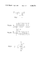
- FIG. 1 shows a conventional wave translating circuit (high-pass filter);
- FIGS. 2A and 2B show waveforms at the input (point a) and at the output (point b), respectively, of the wave translating circuit of FIG. 1;
- FIG. 3 shows another conventional wave translating circuit
- FIGS. 4A and 4B show waveforms at the input (point a) and at the output (point b), respectively, of the wave translating circuit of FIG. 3;
- FIG. 5 shows the first embodiment according to the present invention
- FIGS. 6A, 6B and 6C show waveforms at points e, f and g, respectively, of FIG. 5;
- FIG. 7 shows the second embodiment according to the present invention.
- FIGS. 8A and 8B show waveforms at the input (point h) and at the output (point i), respectively, of the wave translating circuit of FIG. 7 and
- FIGS. 9 and 10 show the third and fourth embodiments according to the present invention, both of which are varieties of the wave translating circuit of FIG. 7.
- the conventional wave translating circuit (high-pass filter) of FIG. 1 has time constant C 1 R 1 formed by capacitor 1 (with capacitance value C 1 ) and load resistor 2 (with resistance value R 1 ).
- the time constant C 1 R 1 must satisfy C 1 R 1 >1/2 ⁇ fp, where fp is the bit rate of pulse waveforms. In the case of continuously generated pulse waveforms no problem arises.
- the transient response of capacitor 1 having time constant C 1 R 1 causes DC component disturbances in output data signals, during the period (T) starting at the instant (t 1 ) of pulse waveform generation as shown in FIG. 2B.
- the wave translating circuit of FIG. 3 has a time constant C 2 R 2 R 3 /(R 2 +R 3 ) formed by capacitor 11 (with capacitance value C 2 ) and resistors 12 and 13 (with resistance value R 2 and R 3 , respectively).
- This time constant must satisfy C 2 R 2 R 3 /(R 2 +R 3 )>1/2 ⁇ fp, where fp is the bit rate of pulse waveforms.
- the DC components of the output voltage in the circuit of FIG. 3 is VR 3 /(R 2 +R 3 ) constant, where V is a voltage applied to one end of resistor 12. If, however, burst signal waveforms as shown in FIG. 4A are applied to point C in FIG.
- the output pulse waveforms shown in FIG. 4B are obtained at point d in FIG. 3.
- the DC components are disturbed for a certain period starting at the instant of pulse waveform generation, due to the transient response of capacitor 11. If data signals having the DC component disturbances as shown in FIGS. 2B and 4B are modulated with a modulator, overmodulation will result with the consequent faulty decision in a code regeneration at the receiver end.
- FIG. 5 shows a wave translating circuit, according to the present invention, immediately following waveform shaping inverters 21 and 22. If pulse waveforms in FIG. 6A are applied to the output (point e) of inverter 22, which is in turn the input of the wave translating circuit, the voltage at point e rises by V/2 (U 1 in FIG. 6A) and hence capacitor 23 is charged in the positive direction. However, because limiter diode 24 conducts, the voltage rise at point f of FIG. 5 is limited to the forward direction voltage V D of diode 24, as shown in FIG. 6B. On the other hand, if the inverter 22 output voltage at point e falls by V/2 (D 1 in FIG.
- variable resistor 25 can be replaced by an adder circuit, such as an operational amplifier.
- limiter diode 34 conducts, limiting the output voltage rise at point i to V+V D , where V D is a forward direction voltage of diode 34 (U 2 in FIG. 8B).
- diode 34 limits the voltage amplitude at their first rise; therefore, almost no DC component transient response occurs at the output (point i).
- the circuit of FIG. 9, which is a variation of the circuit of FIG. 7, is constructed by capacitor 41 (with capacitance value C 4 ), resistors 42 and 43 (with resistance values R 6 and R 7 , respectively) and diode 44.
- This circuit can be used where the high level is constant, in the absence of data pulses. If a data pulse train is applied to the input of the circuit, its waveform starts to fall and then diode 44 conducts, limiting the fall of the output voltage to -V D . Therefore, the DC component transient response can be suppressed.
- the circuit of FIG. 10 is a combination of the circuits of FIGS. 7 and 9 and includes of capacitor 51 (with capacitance value C 5 ), resistors 52 and 53 (with resistance values R 8 and R 9 , respectively) and diodes 54 and 55. This circuit can be used where high or low voltage levels are constant in the absence of data pulses.
- the wave translating circuits enable the suppression of DC component disturbances due to the transient response of capacitors to burst input signals. Therefore, the wave translating circuits according to the invention can be used very effectively as an interface circuit in a transmission system.
Landscapes
- Physics & Mathematics (AREA)
- Nonlinear Science (AREA)
- Dc Digital Transmission (AREA)
Abstract
A wave translating circuit includes a capacitor supplied with an input signal, a first resistor connected between a first potential point and the output of the capacitor, a second resistor connected between a second potential point and the output of the capacitor, and a limiter connected to the output of the capacitor.
Description
The invention relates to a wave translating circuit for supressing transient DC level disturbances of burst data signals generated by a transmitter.
In a transmission system DC level correction of data signals is often conducted, one such example being an adjustment of the operating point of an immediately following amplifier stage.
Several types of wave translating circuits are known, the most widely used of which a high-pass filter circuit comprising a capacitor and a resistor. Although the high-pass filter circuit is simple in construction, the DC components of data signals at the start of transmission and those of burst data signals cannot be removed sufficiently for a certain period due to the transient response of the capacitor. The unremoved portion of the DC components causes overmodulation at the transmitter end of a transmission system and a faulty decision in code regeneration at the receiver end of the transmission system.
It is an object of the present invention to provide a novel wave translating circuit capable of translating the DC components of burst signal waveforms without producing transient disturbances of the DC components.
According to the present invention, there is provided a wave translating circuit, including a capacitor supplied with an input signal, a limiter connected to the output of the capacitor and an adder circuit for adding the output signal of the limiter to the input signal.
According to another aspect of the present invention, there is provided a wave translating circuit including a capacitor supplied with an input signal, a first resistor connected between a first potential point and the output of the capacitor, a second resistor connected between a second potential point and the output of the capacitor, and a limiter connected to the output of the capacitor.
The present invention and its advantages will now be described in detail with reference to the accompanying drawings:
FIG. 1 shows a conventional wave translating circuit (high-pass filter);
FIGS. 2A and 2B show waveforms at the input (point a) and at the output (point b), respectively, of the wave translating circuit of FIG. 1;
FIG. 3 shows another conventional wave translating circuit;
FIGS. 4A and 4B show waveforms at the input (point a) and at the output (point b), respectively, of the wave translating circuit of FIG. 3;
FIG. 5 shows the first embodiment according to the present invention;
FIGS. 6A, 6B and 6C show waveforms at points e, f and g, respectively, of FIG. 5;
FIG. 7 shows the second embodiment according to the present invention;
FIGS. 8A and 8B show waveforms at the input (point h) and at the output (point i), respectively, of the wave translating circuit of FIG. 7 and
FIGS. 9 and 10 show the third and fourth embodiments according to the present invention, both of which are varieties of the wave translating circuit of FIG. 7.
The conventional wave translating circuit (high-pass filter) of FIG. 1 has time constant C1 R1 formed by capacitor 1 (with capacitance value C1) and load resistor 2 (with resistance value R1). The time constant C1 R1 must satisfy C1 R1 >1/2 πfp, where fp is the bit rate of pulse waveforms. In the case of continuously generated pulse waveforms no problem arises. However, for burst signal waveforms as shown in FIG. 2A, the transient response of capacitor 1 having time constant C1 R1 causes DC component disturbances in output data signals, during the period (T) starting at the instant (t1) of pulse waveform generation as shown in FIG. 2B.
The wave translating circuit of FIG. 3 has a time constant C2 R2 R3 /(R2 +R3) formed by capacitor 11 (with capacitance value C2) and resistors 12 and 13 (with resistance value R2 and R3, respectively). This time constant must satisfy C2 R2 R3 /(R2 +R3)>1/2 πfp, where fp is the bit rate of pulse waveforms. In the case of continuously generated pulse waveforms, the DC components of the output voltage in the circuit of FIG. 3 is VR3 /(R2 +R3) constant, where V is a voltage applied to one end of resistor 12. If, however, burst signal waveforms as shown in FIG. 4A are applied to point C in FIG. 3, the output pulse waveforms shown in FIG. 4B are obtained at point d in FIG. 3. As will be obvious from FIG. 4B, the DC components are disturbed for a certain period starting at the instant of pulse waveform generation, due to the transient response of capacitor 11. If data signals having the DC component disturbances as shown in FIGS. 2B and 4B are modulated with a modulator, overmodulation will result with the consequent faulty decision in a code regeneration at the receiver end.
FIG. 5 shows a wave translating circuit, according to the present invention, immediately following waveform shaping inverters 21 and 22. If pulse waveforms in FIG. 6A are applied to the output (point e) of inverter 22, which is in turn the input of the wave translating circuit, the voltage at point e rises by V/2 (U1 in FIG. 6A) and hence capacitor 23 is charged in the positive direction. However, because limiter diode 24 conducts, the voltage rise at point f of FIG. 5 is limited to the forward direction voltage VD of diode 24, as shown in FIG. 6B. On the other hand, if the inverter 22 output voltage at point e falls by V/2 (D1 in FIG. 6A), the voltage at point f also falls from level VD by V/2 (D2 in FIG. 6B). Even if burst data signals are applied in succession to point e, as shown in FIG. 6A, the voltage at point f has almost no DC component transient response, as shown in FIG. 6B. If the voltage at point f is added to the output voltage of inverter 22 by means of variable resistor 25, pulse waveforms are obtained having positive and negative polarities, which can be translated by adjusting their amplitude by means of resistor 26 into positive pulse waveforms, with the DC component removed (FIG. 6C). The input data signal in this case is a positive pulse; however, a negative pulse can provide a similar result if the polarity of diode 24 is reversed. It is apparent that variable resistor 25 can be replaced by an adder circuit, such as an operational amplifier.
If the voltage at the input (point h) of the wave translating circuit of FIG. 7 rises by V (U1 in FIG. 8A), limiter diode 34 conducts, limiting the output voltage rise at point i to V+VD, where VD is a forward direction voltage of diode 34 (U2 in FIG. 8B).
Next, if the voltage at point h falls by V, the output voltage also falls by V from V+VD (D1 and D2 in FIGS. 8A and 8B, respectively).
Even if burst data signals are applied in succession to point h as shown in FIG. 8A, the voltage at point i has almost no DC component transient response as shown in FIG. 8B. The DC component of the output pulses at point i can be given by VR5 /(R4 +R5), where R4 and R5 are resistance values of resistors 32 and 33, respectively (FIG. 8B).
If, for example, rectangular pulse waveforms having constant amplitude referenced to zero voltage are applied to point h, diode 34 limits the voltage amplitude at their first rise; therefore, almost no DC component transient response occurs at the output (point i).
The circuit of FIG. 9, which is a variation of the circuit of FIG. 7, is constructed by capacitor 41 (with capacitance value C4), resistors 42 and 43 (with resistance values R6 and R7, respectively) and diode 44. This circuit can be used where the high level is constant, in the absence of data pulses. If a data pulse train is applied to the input of the circuit, its waveform starts to fall and then diode 44 conducts, limiting the fall of the output voltage to -VD. Therefore, the DC component transient response can be suppressed.
The circuit of FIG. 10 is a combination of the circuits of FIGS. 7 and 9 and includes of capacitor 51 (with capacitance value C5), resistors 52 and 53 (with resistance values R8 and R9, respectively) and diodes 54 and 55. This circuit can be used where high or low voltage levels are constant in the absence of data pulses.
As described in detail above, the wave translating circuits, according to the invention enable the suppression of DC component disturbances due to the transient response of capacitors to burst input signals. Therefore, the wave translating circuits according to the invention can be used very effectively as an interface circuit in a transmission system.
Claims (3)
1. A wave translating circuit comprising capacitor means supplied with an input signal; limiter means for limiting the output of said capacitor means; and adder circuit means for adding the output of said limiter means to said input signal to produce an output signal from said wave translating circuit.
2. The wave translating circuit as claimed in claim 1, wherein said limiter means comprises a rectifier device connected between the output of said capacitor means and a predetermined potential point.
3. The wave translating circuit as claimed in either claim 1 or claim 2, wherein said adder circuit means comprises variable resistance means having input terminals coupled to the output of said limiter means and coupled to receive said input signal, respectively, and an output terminal coupled to the output of said wave translating means.
Applications Claiming Priority (4)
| Application Number | Priority Date | Filing Date | Title |
|---|---|---|---|
| JP53/34320 | 1978-03-24 | ||
| JP53/115329 | 1978-03-24 | ||
| JP3432078A JPS54126452A (en) | 1978-03-24 | 1978-03-24 | Waveform converter circuit |
| JP11532978A JPS5541077A (en) | 1978-09-19 | 1978-09-19 | Waveform conversion circuit |
Publications (1)
| Publication Number | Publication Date |
|---|---|
| US4288751A true US4288751A (en) | 1981-09-08 |
Family
ID=33031543
Family Applications (1)
| Application Number | Title | Priority Date | Filing Date |
|---|---|---|---|
| US06/022,648 Expired - Lifetime US4288751A (en) | 1978-03-24 | 1979-03-21 | Wave translating circuit |
Country Status (1)
| Country | Link |
|---|---|
| US (1) | US4288751A (en) |
Cited By (3)
| Publication number | Priority date | Publication date | Assignee | Title |
|---|---|---|---|---|
| DE3623735A1 (en) * | 1985-07-19 | 1987-01-22 | Hitachi Ltd | SIGNAL TRANSFER CIRCUIT |
| US4639936A (en) * | 1984-02-10 | 1987-01-27 | Prime Computer, Inc. | Data transmission signal apparatus |
| EP0818785A3 (en) * | 1996-07-11 | 1998-12-30 | Texas Instruments Incorporated | A method and apparatus for detecting and removing additive transient disturbances |
Citations (3)
| Publication number | Priority date | Publication date | Assignee | Title |
|---|---|---|---|---|
| US3237019A (en) * | 1961-06-28 | 1966-02-22 | Ibm | Electronic clamping circuit |
| US3248658A (en) * | 1963-03-14 | 1966-04-26 | Ibm | Detector for information signals having an extremely low signal-to-noise ratio |
| US3463940A (en) * | 1966-02-02 | 1969-08-26 | Northern Electric Co | D.c. restoration circuit |
-
1979
- 1979-03-21 US US06/022,648 patent/US4288751A/en not_active Expired - Lifetime
Patent Citations (3)
| Publication number | Priority date | Publication date | Assignee | Title |
|---|---|---|---|---|
| US3237019A (en) * | 1961-06-28 | 1966-02-22 | Ibm | Electronic clamping circuit |
| US3248658A (en) * | 1963-03-14 | 1966-04-26 | Ibm | Detector for information signals having an extremely low signal-to-noise ratio |
| US3463940A (en) * | 1966-02-02 | 1969-08-26 | Northern Electric Co | D.c. restoration circuit |
Non-Patent Citations (1)
| Title |
|---|
| Pulse, Digital, and Switching Waveforms by Millman & Taub, Copyright 1965, Chapter 8 "Clamping and Switching Circuits", pp. 262-277. * |
Cited By (4)
| Publication number | Priority date | Publication date | Assignee | Title |
|---|---|---|---|---|
| US4639936A (en) * | 1984-02-10 | 1987-01-27 | Prime Computer, Inc. | Data transmission signal apparatus |
| DE3623735A1 (en) * | 1985-07-19 | 1987-01-22 | Hitachi Ltd | SIGNAL TRANSFER CIRCUIT |
| US4723082A (en) * | 1985-07-19 | 1988-02-02 | Hitachi, Ltd. | Signal transfer circuit for use in laminated multilayer electric circuit |
| EP0818785A3 (en) * | 1996-07-11 | 1998-12-30 | Texas Instruments Incorporated | A method and apparatus for detecting and removing additive transient disturbances |
Similar Documents
| Publication | Publication Date | Title |
|---|---|---|
| US4339727A (en) | Waveform converting circuit | |
| US4835486A (en) | Isolation amplifier with precise timing of signals coupled across isolation barrier | |
| US5804993A (en) | Detecting circuit | |
| US4288751A (en) | Wave translating circuit | |
| US4609839A (en) | Noise inverter circuit for a power line communication system | |
| US4652774A (en) | Rectangular wave-shaping circuit with varying threshold level | |
| GB2154105A (en) | Transceivers | |
| KR920003510Y1 (en) | Receiver for digital audio signal | |
| EP0202601A2 (en) | Optical pulse receiving circuit | |
| JPS6110312A (en) | Signal converter circuit | |
| US3619651A (en) | Digital frequency discriminator | |
| US4034240A (en) | Sine-to-square wave converter | |
| JPS6129172B2 (en) | ||
| US3946253A (en) | Pulse train generator | |
| JP2723029B2 (en) | Automatic threshold control circuit | |
| JP3239185B2 (en) | Level measuring device | |
| US6445219B1 (en) | Method and circuit configuration for converting a frequency signal to a DC voltage | |
| JPH0254695B2 (en) | ||
| US5097143A (en) | Bipolar to unipolar converter with automatic gain control | |
| JPH0775336B2 (en) | Optical receiver circuit | |
| KR860001349Y1 (en) | Interface device for cassette tape record of personal computer | |
| JPH04302525A (en) | Pulse demodulating circuit | |
| JPS6380613A (en) | Simplified device for generating tone signal | |
| JPH0441531B2 (en) | ||
| JPS5814095B2 (en) | Waveform shaping circuit |
Legal Events
| Date | Code | Title | Description |
|---|---|---|---|
| STCF | Information on status: patent grant |
Free format text: PATENTED CASE |