US4250488A - Device for scanning patterns with a regulated light source - Google Patents
Device for scanning patterns with a regulated light source Download PDFInfo
- Publication number
- US4250488A US4250488A US06/029,017 US2901779A US4250488A US 4250488 A US4250488 A US 4250488A US 2901779 A US2901779 A US 2901779A US 4250488 A US4250488 A US 4250488A
- Authority
- US
- United States
- Prior art keywords
- resistor
- light source
- comparator
- voltage
- collector
- Prior art date
- Legal status (The legal status is an assumption and is not a legal conclusion. Google has not performed a legal analysis and makes no representation as to the accuracy of the status listed.)
- Expired - Lifetime
Links
Images
Classifications
-
- G—PHYSICS
- G06—COMPUTING OR CALCULATING; COUNTING
- G06K—GRAPHICAL DATA READING; PRESENTATION OF DATA; RECORD CARRIERS; HANDLING RECORD CARRIERS
- G06K7/00—Methods or arrangements for sensing record carriers, e.g. for reading patterns
- G06K7/10—Methods or arrangements for sensing record carriers, e.g. for reading patterns by electromagnetic radiation, e.g. optical sensing; by corpuscular radiation
- G06K7/10544—Methods or arrangements for sensing record carriers, e.g. for reading patterns by electromagnetic radiation, e.g. optical sensing; by corpuscular radiation by scanning of the records by radiation in the optical part of the electromagnetic spectrum
- G06K7/10821—Methods or arrangements for sensing record carriers, e.g. for reading patterns by electromagnetic radiation, e.g. optical sensing; by corpuscular radiation by scanning of the records by radiation in the optical part of the electromagnetic spectrum further details of bar or optical code scanning devices
- G06K7/10881—Methods or arrangements for sensing record carriers, e.g. for reading patterns by electromagnetic radiation, e.g. optical sensing; by corpuscular radiation by scanning of the records by radiation in the optical part of the electromagnetic spectrum further details of bar or optical code scanning devices constructional details of hand-held scanners
-
- G—PHYSICS
- G06—COMPUTING OR CALCULATING; COUNTING
- G06V—IMAGE OR VIDEO RECOGNITION OR UNDERSTANDING
- G06V10/00—Arrangements for image or video recognition or understanding
- G06V10/10—Image acquisition
- G06V10/12—Details of acquisition arrangements; Constructional details thereof
- G06V10/14—Optical characteristics of the device performing the acquisition or on the illumination arrangements
- G06V10/145—Illumination specially adapted for pattern recognition, e.g. using gratings
-
- H—ELECTRICITY
- H04—ELECTRIC COMMUNICATION TECHNIQUE
- H04N—PICTORIAL COMMUNICATION, e.g. TELEVISION
- H04N1/00—Scanning, transmission or reproduction of documents or the like, e.g. facsimile transmission; Details thereof
- H04N1/40—Picture signal circuits
- H04N1/40056—Circuits for driving or energising particular reading heads or original illumination means
-
- G—PHYSICS
- G06—COMPUTING OR CALCULATING; COUNTING
- G06K—GRAPHICAL DATA READING; PRESENTATION OF DATA; RECORD CARRIERS; HANDLING RECORD CARRIERS
- G06K2207/00—Other aspects
- G06K2207/1018—Source control
Definitions
- the invention relates to a device for scanning patterns with a light source which illuminates a scanning field on a recording medium, and in particular in which a sensor is formed of a plurality of photoelectric elements for converting the reflected light received from the scanning field, via a lens, into analog electric image signals, in which the light flux emitted by the light source is automatically readjusted for the compensation of interference factors.
- Such scanning devices are employed in automatic character recognition systems in order to convert visually readable ciphers or letters of a recording medium, for example, of a document, of a letter or even of a label, directly into a form that can be evaluated by machine and to supply the characters for further processing to a data processing system.
- a scanning device of the type generally mentioned above is known, for example, from the German allowed application No. 2,534,235.
- a photo diode line having a built-in sampling shift register is employed as the sensor surface.
- An analog-digital converter is connected to the sensor by way of an integrator, the output signals of which represent digitized image signals.
- These signals are subject to error by differences in the electron yield of the individual photo diodes, by differences in the light-sensitive surfaces of the diodes, by unevenness of the light and other systematic errors. The errors must therefore be eliminated before further processing of the image signals in a recognition device.
- the white background of the read zone of a recording medium to be scanned is directly employed for the simulation of a calibration norm.
- This uniform surface is scanned for the preparation of correction values for the image signals.
- a correction value respectively allocated to a specific photo diode is calculated from the scanning signals thus generated and incorrectly deviating from one another by means of an individual comparison with a reference value.
- a gray scale value storage is additionally provided, which intermediately stores the scanned digitized image signals until a first calculation of the correction values is accomplished.
- the recording medium to be read must be illuminated in a character recognition device.
- the brightness respectively returned from the scanning field of the recording medium is imaged via an optic on a sensor surface which converts the brightness into electrical signals.
- the fluctuation of the returned brightness stems, on the one hand, from the characters on the recording medium and contains the desired information. On the other hand, however, it contains undesired information caused by interference factors which are caused by the aging of the illumination and by the changing diffused reflectance of the background and the like.
- an electro-optical control loop for regulating the intensity of the spot of light of a cathode ray tube is known from the German Pat. No. 1,917,006.
- cathode ray tubes were more often employed as flying-spot scanners because they allow a point of light, sharply focused on the screen of the cathode ray tube, to be easily deflected, at least in one direction.
- This point of light is imaged by means of a lens onto the scanning field with the recording medium as the picture plane.
- the reflected light is converted into electrical image signals with very sensitive photoelectric transducers, for example photo multipliers.
- the flying-spot scanners find little use today.
- the cathode ray tube requires a large spatial volume, is only a very weak light source, and therefore requires very sensitive photoelectric elements whose varying sensitivity moreover falsify the scanning result given different light incidence angles of the light return from the scanning field.
- the influences of the varying reflectivity of the individual recording medium is compensated, on the one hand and, on the other hand, separately from this, the modulation of the image signals to be traced to the varying angle of incidence of the reflected light is eliminated.
- a separate control loop is provided for this purpose.
- a second pair of photo multipliers which are not oriented toward the scanning field, but rather toward the screen of the cathode ray tube, are part of this control loop.
- the common output of this second pair of transducers is connected to a control circuit in which a signal for controlling the radiation intensity of the cathode ray tube is derived from the common transducer signal by means of comparison with a reference voltage in such a manner that the second pair of transducers emits a signal which is adapted to the reference voltage as much as possible.
- Flying-spot scanners which exhibit additional photoelectric transducers in order to generate an adjustment magnitude in a control loop which serves to control the intensity of the point of light on the screen of the cathode ray tube in such a manner that varying angles of light incidence of the reflected light on the photoelectric transducers scanning the field of the recording medium are compensated are therefore to be presumed as known in character recognition devices which utilize automatic document transport.
- control loop known in this connection is also far too expensive in its basic construction for character recognition devices which are to be peripherally employed and be as cost-effective as possible. In the known installation, one has proceeded precisely from that consideration of duplicating the entire arrangement for the photo-electric conversion of the scanning signal in order to create a separate control loop.
- the object of the present invention is to provide a device of the type generally mentioned above with which it is possible to eliminate the undesired information in the scanning signal produced by the fluctuating reflectivity of the recording medium and by the changing distance of the recording medium from the light source by regulating the intensity of the illumination.
- This object is achieved, in a device of the type generally mentioned above, by providing that the sensor sum the individual analog image signals and provide the same, through a time delay device, to a comparator circuit for comparison with a fixed reference voltage.
- the comparator circuit is connected with a control input of a regulating unit with which the lamp voltage of the light source can be adjusted as a function of the output signal of the comparator circuit.
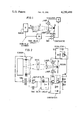
- FIG. 1 is a block diagram of a device constructed in accordance with the present invention for scanning patterns and having a regulated light source which compensates for interference factors;
- FIG. 2 is a detailed circuit diagram of the apparatus illustrated in FIG. 1.
- a recording medium A is schematically illustrated.
- two lamps L are arranged in a parallel plane in such a manner that they illuminate a limited scanning field on the recording medium A under an angle of about 45°.
- the light RL reflected from the recording medium is directed by way of a lens O, to strike a sensor surface SF, i.e. the scanning field is thus imaged on the sensor surface SF.
- the sensor comprises a plurality of photoelectric elements which can be arranged in a line or in the form of a matrix.
- the brightness received by the sensor and converted into electric signals is supplied as a measurable value to a time delay device VG which serves for the separation of the rapidly changing desired character information from the undesired interference factors.
- the measurable variable formed in this manner is supplied to a comparator circuit VS and is there compared with a reference value SW.
- the output signal of the comparator VS then forms an adjustment magnitude which is supplied to a regulating unit SG which regulates the brightness of the lamps L via their operating voltage as a function of the controlling input magnitude.
- the control loop is closed via the optical path of the reflected light RL beamed from the lamps L onto the scanning field of the recording medium A and reflected therefrom to the sensor.
- FIG. 2 is a detailed circuit illustration of an arrangement for the control loop described, in principle, on the basis of FIG. 1.
- the locally incident reflected light RL is converted into proportional currents in the photo sensitive sensor SF, which currents flow from a positive voltage source +UB into the photoelectric transducer via load resistors R1-R16 respectively assigned to a photo sensitive element or to a plurality of photo sensitive elements.
- a further ohmic resistor R17 is connected between a common junction of the resistors R1-R16 and the positive voltage source +UB as a terminal resistance which is traversed by the sum of the photo currents. The voltage decrease at this terminal resistor R17 forms the measurable variable for the control loop.
- a further ohmic resistor R18 is connected in common with the resistor R17 to the positive voltage source +UB.
- the resistors R17 and R18 are connected at their other ends to a respective input of an amplifier V which has a further ohmic resistor R19 connected as a feedback resistor between the output of the amplifier V and the input which is connected to the resistor R18.
- the measurable variable occurring as a voltage drop at the resistor R17 is amplified by the amplifier V in the ratio of the feedback resistor R19 to the input resistor R18.
- the measurable value amplified in this manner is supplied to the time delay device VG which is designed as a low-pass filter and which has a further ohmic resistor R20 in a series arm and a bypass capacitor C connected to ground in a shunt arm.
- the low-pass filter is dimensioned in such a manner that all high-frequency portions of the amplified measurable value are filtered out and only its low-frequency portions are to be allocated to and considered to represent interference factors which are to be further processed.
- the filtered measurable variable is supplied to the comparator circuit VS.
- the comparator circuit VS is designed as a differential amplifier and comprises two transistors T1 and T2 whose emitters are connected to a negative voltage source -UB by way of a common emitter resistor R21.
- the first transistor T1 has its base connected to the output of the time delay device VG and has its collector connected to the positive voltage source +UB.
- the reference value SW is supplied to the base of the second transistor T2 as a comparison value.
- the reference value is generated with a permanently adjusted voltage divider which comprises two further ohmic resistors R22 and R23 which are connected in series between the positive voltage +UB and ground.
- the collector of the second transistor T2 forms the output of the comparator circuit VS and is connected to the regulator circuit SG.
- the regulating circuit SG comprises a further transistor T3 whose base is connected to the output of the comparator circuit VS.
- a further ohmic resistor R24 is connected in parallel to the emitter-collector path of the transistor T3 and in series therewith between the positive voltage source +UB and the lamps L1 and L2 which are connected in parallel to each other between the resistor R24 and ground.
- the transistor T3 of the regulating unit SG is modulated according to the control signal supplied to its base and, therefore, the current supplied from the positive voltage source +UB for the lamps L1 and L2 is accordingly regulated.
Landscapes
- Engineering & Computer Science (AREA)
- Physics & Mathematics (AREA)
- Theoretical Computer Science (AREA)
- Computer Vision & Pattern Recognition (AREA)
- General Physics & Mathematics (AREA)
- Multimedia (AREA)
- Artificial Intelligence (AREA)
- Electromagnetism (AREA)
- Signal Processing (AREA)
- Health & Medical Sciences (AREA)
- General Health & Medical Sciences (AREA)
- Toxicology (AREA)
- Character Input (AREA)
Applications Claiming Priority (2)
| Application Number | Priority Date | Filing Date | Title |
|---|---|---|---|
| DE19782816325 DE2816325A1 (de) | 1978-04-14 | 1978-04-14 | Einrichtung zum abtasten von mustern mit einer geregelten lichtquelle |
| DE2816325 | 1978-04-14 |
Publications (1)
| Publication Number | Publication Date |
|---|---|
| US4250488A true US4250488A (en) | 1981-02-10 |
Family
ID=6037026
Family Applications (1)
| Application Number | Title | Priority Date | Filing Date |
|---|---|---|---|
| US06/029,017 Expired - Lifetime US4250488A (en) | 1978-04-14 | 1979-04-11 | Device for scanning patterns with a regulated light source |
Country Status (3)
| Country | Link |
|---|---|
| US (1) | US4250488A (de) |
| EP (1) | EP0004852B1 (de) |
| DE (1) | DE2816325A1 (de) |
Cited By (24)
| Publication number | Priority date | Publication date | Assignee | Title |
|---|---|---|---|---|
| US4414546A (en) * | 1979-10-16 | 1983-11-08 | Robert G. Boorman | Apparatus for and methods of identifying horses by scanning their chestnuts |
| US4481667A (en) * | 1981-12-21 | 1984-11-06 | Autronics Corporation | Item counting apparatus |
| US4499595A (en) * | 1981-10-01 | 1985-02-12 | General Electric Co. | System and method for pattern recognition |
| US4536648A (en) * | 1984-07-30 | 1985-08-20 | Ncr Corporation | Optical card read/write scanning system |
| US4538072A (en) * | 1982-04-20 | 1985-08-27 | Siemens Aktiengesellschaft | Optical wand for reading OCR characters and bar code marks |
| US4634933A (en) * | 1983-12-05 | 1987-01-06 | Kabushiki Kaisha Sunpak | Photographic illumination apparatus |
| US4649267A (en) * | 1984-04-26 | 1987-03-10 | Ilc Technology, Inc. | Automatic gain control circuit for encoder |
| US4673805A (en) * | 1982-01-25 | 1987-06-16 | Symbol Technologies, Inc. | Narrow-bodied, single- and twin-windowed portable scanning head for reading bar code symbols |
| US4677287A (en) * | 1982-07-14 | 1987-06-30 | Canon Kabushiki Kaisha | Document reader with light source control |
| US4718768A (en) * | 1984-05-10 | 1988-01-12 | Dainippon Screen Mfg. Co., Ltd. | Image data correction |
| EP0222559A3 (en) * | 1985-10-31 | 1989-03-08 | Minnesota Mining And Manufacturing Company | Apparatus for electronic scanning and microfilming of documents |
| US4825065A (en) * | 1985-10-31 | 1989-04-25 | Canon Kabushiki Kaisha | Apparatus for reading image recorded on film |
| US4970379A (en) * | 1987-04-30 | 1990-11-13 | Norand Corporation | Bar code scanner system and scanner circuitry therefor |
| US4995090A (en) * | 1989-02-07 | 1991-02-19 | The University Of Michigan | Optoelectronic pattern comparison system |
| US5105071A (en) * | 1990-01-09 | 1992-04-14 | Tokyo Electric Co., Ltd. | Optical data transfer device |
| EP0378199A3 (de) * | 1989-01-10 | 1993-09-01 | Sumitomo Electric Industries, Ltd. | Marken-Lesegerät |
| EP0585595A3 (de) * | 1992-09-03 | 1994-10-12 | Lre Relais & Elektronik Gmbh | Verfahren und Einrichtung zum Lesen binärer Informationen. |
| US5550362A (en) * | 1992-11-20 | 1996-08-27 | Intermec Corporation | Method and apparatus for calibrating a bar code scanner |
| US5696370A (en) * | 1995-02-28 | 1997-12-09 | Psc Inc. | Bar code scanning system for automatically calculating the optical power output levels of the light source |
| US5791771A (en) * | 1995-12-19 | 1998-08-11 | United Parcel Service Of America, Inc. | Unsymmetrical elliptical reflector for spatial illumination |
| US5808286A (en) * | 1995-06-05 | 1998-09-15 | Asahi Kogaku Kogyo Kabushiki Kaisha | Data symbol reader utilizing ambient light illumination |
| US6292595B1 (en) * | 1997-05-22 | 2001-09-18 | Zih Corporation | Image recording device |
| US6329647B1 (en) | 2000-07-03 | 2001-12-11 | Peter J. Mikan | Compensation reference circuit for opto-mechanical joystick |
| US20080135737A1 (en) * | 2006-12-11 | 2008-06-12 | Innolux Display Corp. | Light source device and method for modulating brightness of light emitted by same and liquid crystal display using same |
Families Citing this family (3)
| Publication number | Priority date | Publication date | Assignee | Title |
|---|---|---|---|---|
| DE3213769A1 (de) * | 1982-04-14 | 1983-10-27 | Datronic Gesellschaft für Informationsverarbeitung mbH, 8902 Neusäß | Verfahren zum herstellen von mikrofilmen sowie derart hergestellter mikrofilm |
| JPS63166355A (ja) * | 1986-12-27 | 1988-07-09 | Sharp Corp | 読取り装置 |
| DE10160843B4 (de) * | 2001-12-12 | 2005-12-29 | Daimlerchrysler Ag | Biometrisches Erkennungssystem |
Citations (10)
| Publication number | Priority date | Publication date | Assignee | Title |
|---|---|---|---|---|
| US3089123A (en) * | 1959-11-12 | 1963-05-07 | Ibm | Character recognition quantizing apparatus |
| US3322893A (en) * | 1963-12-11 | 1967-05-30 | Xerox Corp | Background scanning system for facsimile communication |
| US3449585A (en) * | 1966-02-15 | 1969-06-10 | Arnold Trehub | Automatic recognition system using constant intensity image bearing light beam |
| US3517167A (en) * | 1966-12-28 | 1970-06-23 | Bell & Howell Co | Feedback light control system |
| US3582661A (en) * | 1967-09-25 | 1971-06-01 | Philips Corp | Photoelectric yarn measurer having reference channel |
| GB1241404A (en) * | 1969-04-02 | 1971-08-04 | Siemens Ag | Improvements in or relating to cathode ray tube optical data scanners |
| US3651252A (en) * | 1970-01-22 | 1972-03-21 | Polaroid Corp | Image reproduction system which detects subject by sensing intensity ratios |
| US3944979A (en) * | 1974-12-23 | 1976-03-16 | Data Source Corporation | Method and apparatus for illuminating an object bearing indicia |
| US4143358A (en) * | 1974-01-07 | 1979-03-06 | Recognition Equipment Incorporated | Wand lamp control |
| US4177449A (en) * | 1977-01-27 | 1979-12-04 | Hitachi, Ltd. | Photoelectric converter apparatus |
Family Cites Families (2)
| Publication number | Priority date | Publication date | Assignee | Title |
|---|---|---|---|---|
| US3760162A (en) * | 1969-11-13 | 1973-09-18 | Smiths Industries Ltd | Photoelectric readers |
| US4101072A (en) * | 1976-10-21 | 1978-07-18 | The Singer Company | Data-gathering device for scanning data having a variable amplitude modulation and signal to noise ratio |
-
1978
- 1978-04-14 DE DE19782816325 patent/DE2816325A1/de not_active Ceased
-
1979
- 1979-02-08 EP EP79100366A patent/EP0004852B1/de not_active Expired
- 1979-04-11 US US06/029,017 patent/US4250488A/en not_active Expired - Lifetime
Patent Citations (10)
| Publication number | Priority date | Publication date | Assignee | Title |
|---|---|---|---|---|
| US3089123A (en) * | 1959-11-12 | 1963-05-07 | Ibm | Character recognition quantizing apparatus |
| US3322893A (en) * | 1963-12-11 | 1967-05-30 | Xerox Corp | Background scanning system for facsimile communication |
| US3449585A (en) * | 1966-02-15 | 1969-06-10 | Arnold Trehub | Automatic recognition system using constant intensity image bearing light beam |
| US3517167A (en) * | 1966-12-28 | 1970-06-23 | Bell & Howell Co | Feedback light control system |
| US3582661A (en) * | 1967-09-25 | 1971-06-01 | Philips Corp | Photoelectric yarn measurer having reference channel |
| GB1241404A (en) * | 1969-04-02 | 1971-08-04 | Siemens Ag | Improvements in or relating to cathode ray tube optical data scanners |
| US3651252A (en) * | 1970-01-22 | 1972-03-21 | Polaroid Corp | Image reproduction system which detects subject by sensing intensity ratios |
| US4143358A (en) * | 1974-01-07 | 1979-03-06 | Recognition Equipment Incorporated | Wand lamp control |
| US3944979A (en) * | 1974-12-23 | 1976-03-16 | Data Source Corporation | Method and apparatus for illuminating an object bearing indicia |
| US4177449A (en) * | 1977-01-27 | 1979-12-04 | Hitachi, Ltd. | Photoelectric converter apparatus |
Cited By (27)
| Publication number | Priority date | Publication date | Assignee | Title |
|---|---|---|---|---|
| US4414546A (en) * | 1979-10-16 | 1983-11-08 | Robert G. Boorman | Apparatus for and methods of identifying horses by scanning their chestnuts |
| US4499595A (en) * | 1981-10-01 | 1985-02-12 | General Electric Co. | System and method for pattern recognition |
| US4481667A (en) * | 1981-12-21 | 1984-11-06 | Autronics Corporation | Item counting apparatus |
| US4673805A (en) * | 1982-01-25 | 1987-06-16 | Symbol Technologies, Inc. | Narrow-bodied, single- and twin-windowed portable scanning head for reading bar code symbols |
| US4538072A (en) * | 1982-04-20 | 1985-08-27 | Siemens Aktiengesellschaft | Optical wand for reading OCR characters and bar code marks |
| US4677287A (en) * | 1982-07-14 | 1987-06-30 | Canon Kabushiki Kaisha | Document reader with light source control |
| US4634933A (en) * | 1983-12-05 | 1987-01-06 | Kabushiki Kaisha Sunpak | Photographic illumination apparatus |
| US4649267A (en) * | 1984-04-26 | 1987-03-10 | Ilc Technology, Inc. | Automatic gain control circuit for encoder |
| US4718768A (en) * | 1984-05-10 | 1988-01-12 | Dainippon Screen Mfg. Co., Ltd. | Image data correction |
| US4536648A (en) * | 1984-07-30 | 1985-08-20 | Ncr Corporation | Optical card read/write scanning system |
| EP0222559A3 (en) * | 1985-10-31 | 1989-03-08 | Minnesota Mining And Manufacturing Company | Apparatus for electronic scanning and microfilming of documents |
| US4825065A (en) * | 1985-10-31 | 1989-04-25 | Canon Kabushiki Kaisha | Apparatus for reading image recorded on film |
| US4970379A (en) * | 1987-04-30 | 1990-11-13 | Norand Corporation | Bar code scanner system and scanner circuitry therefor |
| EP0378199A3 (de) * | 1989-01-10 | 1993-09-01 | Sumitomo Electric Industries, Ltd. | Marken-Lesegerät |
| US4995090A (en) * | 1989-02-07 | 1991-02-19 | The University Of Michigan | Optoelectronic pattern comparison system |
| US5105071A (en) * | 1990-01-09 | 1992-04-14 | Tokyo Electric Co., Ltd. | Optical data transfer device |
| EP0585595A3 (de) * | 1992-09-03 | 1994-10-12 | Lre Relais & Elektronik Gmbh | Verfahren und Einrichtung zum Lesen binärer Informationen. |
| US5550362A (en) * | 1992-11-20 | 1996-08-27 | Intermec Corporation | Method and apparatus for calibrating a bar code scanner |
| US5834750A (en) * | 1995-02-28 | 1998-11-10 | Psc, Inc. | Bar code scanning system for automatically maintaining constant the amplitude of light reflected from a bar code |
| US5696370A (en) * | 1995-02-28 | 1997-12-09 | Psc Inc. | Bar code scanning system for automatically calculating the optical power output levels of the light source |
| GB2302405B (en) * | 1995-06-05 | 1999-12-01 | Asahi Optical Co Ltd | Data symbol reader |
| US5808286A (en) * | 1995-06-05 | 1998-09-15 | Asahi Kogaku Kogyo Kabushiki Kaisha | Data symbol reader utilizing ambient light illumination |
| US5791771A (en) * | 1995-12-19 | 1998-08-11 | United Parcel Service Of America, Inc. | Unsymmetrical elliptical reflector for spatial illumination |
| US6292595B1 (en) * | 1997-05-22 | 2001-09-18 | Zih Corporation | Image recording device |
| US6329647B1 (en) | 2000-07-03 | 2001-12-11 | Peter J. Mikan | Compensation reference circuit for opto-mechanical joystick |
| US20080135737A1 (en) * | 2006-12-11 | 2008-06-12 | Innolux Display Corp. | Light source device and method for modulating brightness of light emitted by same and liquid crystal display using same |
| US7786420B2 (en) * | 2006-12-11 | 2010-08-31 | Chimei Innolux Corporation | Light source device and method for modulating brightness of light emitted by same and liquid crystal display using same |
Also Published As
| Publication number | Publication date |
|---|---|
| EP0004852B1 (de) | 1982-05-12 |
| EP0004852A1 (de) | 1979-10-31 |
| DE2816325A1 (de) | 1979-10-18 |
Similar Documents
| Publication | Publication Date | Title |
|---|---|---|
| EP0004852B1 (de) | Einrichtung zum Abtasten von Mustern mit einer geregelten Lichtquelle | |
| US5138623A (en) | Semiconductor laser control device | |
| EP0627151A1 (de) | Verfahren und vorrichtung zur dynamischen korrektur von mikroskopischen bildsignalen | |
| US5108176A (en) | Method of calibrating scanners and arrangement for producing defined scattered light amplitudes | |
| NL8200517A (nl) | Instelschakeling voor licht-emitterende diode met temperatuurcompensatie. | |
| US3580683A (en) | Computing colorimeter | |
| JP2000171295A (ja) | Apdバイアス回路 | |
| US4745488A (en) | Image reader | |
| US3171032A (en) | Photomultiplier with stabilized gain | |
| US5117119A (en) | Auto-ranging film densitometer | |
| US3626092A (en) | Video amplifier for optical scanners | |
| US4484079A (en) | Registration mark detector | |
| US4536091A (en) | Absorbance monitor | |
| GB2083313A (en) | Distance detecting device | |
| US5130822A (en) | Method and apparatus for correcting an image signal | |
| US5859429A (en) | Optical system with test/calibration | |
| US4938588A (en) | Distance detecting apparatus | |
| US3987413A (en) | Detection system | |
| JP2551344B2 (ja) | 媒体検出用フォトセンサ回路 | |
| JPH0638069B2 (ja) | 示差屈折計 | |
| JP2569485B2 (ja) | レ−ザ回折光の強度分布測定装置 | |
| JPS5945087B2 (ja) | 光電素子の感度補正回路 | |
| JPS6151820B2 (de) | ||
| JPS5820064A (ja) | 自動コントラスト調整回路 | |
| JPH03107709A (ja) | 光学的測定装置 |