US3961143A - Multi-frequency signalling system - Google Patents
Multi-frequency signalling system Download PDFInfo
- Publication number
- US3961143A US3961143A US05/505,014 US50501474A US3961143A US 3961143 A US3961143 A US 3961143A US 50501474 A US50501474 A US 50501474A US 3961143 A US3961143 A US 3961143A
- Authority
- US
- United States
- Prior art keywords
- circuit
- transistor
- frequency
- tuned
- signalling system
- Prior art date
- Legal status (The legal status is an assumption and is not a legal conclusion. Google has not performed a legal analysis and makes no representation as to the accuracy of the status listed.)
- Expired - Lifetime
Links
Images


Classifications
-
- H—ELECTRICITY
- H04—ELECTRIC COMMUNICATION TECHNIQUE
- H04Q—SELECTING
- H04Q1/00—Details of selecting apparatus or arrangements
- H04Q1/18—Electrical details
- H04Q1/30—Signalling arrangements; Manipulation of signalling currents
- H04Q1/44—Signalling arrangements; Manipulation of signalling currents using alternate current
- H04Q1/444—Signalling arrangements; Manipulation of signalling currents using alternate current with voice-band signalling frequencies
- H04Q1/45—Signalling arrangements; Manipulation of signalling currents using alternate current with voice-band signalling frequencies using multi-frequency signalling
- H04Q1/453—Signalling arrangements; Manipulation of signalling currents using alternate current with voice-band signalling frequencies using multi-frequency signalling in which m-out-of-n signalling frequencies are transmitted
Definitions
- the present invention relates to a multiple-frequency signalling system including multiple-frequency sender means which are coupled to multiple-frequency receiver means via a transmission path.
- the sender is adapted to generate a plurality of alternating signals having different frequencies.
- the receiver means includes an evaluating circuit to evaluate the presence of a predetermined number of said alternating signals received by said receiver means.
- Said receiver means further including a plurality of channel paths each including a filter tuned to a frequency of said alternating signals and inhibiting means which render said channel paths ineffective upon spurious signals being applied to them.
- the channel path being rendered effective when simultaneously said channel path receives a signal having a frequency equal to that to which the filter included in this channel path is tuned and said evaluating circuit evaluates a said predetermined number of alternating signals.
- Such a system is known from the U.S. Pat. No. 3,072,747. Therein digits are each transmitted in the form of a combination of two alternating signals out of a plurality of six such signals.
- the inhibiting means included in each channel path of this system comprise an additional filter or rejector circuit accepting said plurality of frequencies but having a rectified output which is in opposition to the rectified output of the filter included in this channel path and tuned to a particular one of this plurality of frequencies.
- spurious signals are received by the receiver means the rejector circuit of each channel path rectified output of this circuit overrides that of the tuned filter included in this path and inhibits the latter.
- Such an erroneous operation is however eliminated by the use of a band-stop filter tuned to the frequency F2 preventing the frequency signal having this frequency F2 from reaching the rejector circuit.
- a band-stop filter tuned to the frequency F2 preventing the frequency signal having this frequency F2 from reaching the rejector circuit.
- This band-stop filter is tuned to the common frequency of the group and precedes a group of channel paths each including a filter tuned to a distinct non-common frequency of the combinations of that group.
- Table 2 of the above mentioned U.S. patent shows the grouping of frequencies in four groups.
- Each of these groups contains a common or band-stop filter frequency F2; F3; F4; F5 and noncommon or acceptor frequencies F1, F3, F4, F5; F1, F5, F6; F1 F3; F1, F4, F6 respectively.
- each of the twelve channel paths moreover includes an additional filter or rejector circuit, while each of the four groups of tuned filters is preceded by a band-stop filter.
- the known system includes a relatively large number of filters which have moreover to be of good quality to assure good stability and which are therefore relatively expensive.
- the present multiple-frequency signalling system is characterized in that the inhibiting means included in each of said channel paths include a detection circuit coupled between the tuned filter included in this path and said evaluating circuit and able to compare a voltage value provided by this filter with a threshold voltage value, said detection circuit being able to react when the difference between the compared voltages reaches a predetermined value, and that the operation of said evaluation circuit is prevented when at least one of said detection circuits reacts, thus rendering said channel paths ineffective.
- the tuned filters in each of the channel paths pass the frequency to which they are tuned when spurious signals of a broad spectrum are received and at least one detection circuit coupled to the corresponding tuned filter will react when the voltage value at this tuned filter is larger than said threshold voltage value. Since no rejector filters are required also no band-stop filters are needed. As mentioned above, the introduction of these rejector and band-stop filters entails the necessity to have a number of channel paths larger than said plurality of frequency signals. This number can thus be reduced by eliminating the above mentioned filters. Moreover, the presence of one detection circuit per channel path and of an evaluating circuit able to evaluate the presence of said predetermined number of frequency signals permits to use one channel path per frequency signal so that also the number of tuned filters is reduced.
- FIG. 1 is a block diagram of a receiver forming part of a signalling and detection system according to the invention
- FIG. 2 and FIG. 3 show detailed circuits of the above receiver
- FIG. 4 is a diagram showing frequency signals which facilitate the understanding of the operation of the circuits shown in FIGS. 2 and 3;
- FIG. 5 is a diagram showing the envelopes of other signals capable of being produced in the circuits of FIGS. 2 and 3.
- the receiver shown therein forms part of a multiple frequency signalling system such as described in the Belgian patent 646,658 (G. Thyssens-2) and in the article "Interregister Multi-frequency-code signalling for telephone switching in Europe" of M. den Hertog published in "Electrical Communication” vol. 38, No. 1, 1963.
- Digit or other information is transmitted by means of a combination of a number of frequencies selected from a plurality of available frequencies. For example, each digit information may be transmitted by means of two signals each having a frequency chosen out of a group of five voice frequencies f1 to f5. These combinations have to be recognized by the receiver.
- the input signals at the input terminal IN are fed to each individual receiver IRi via the multiple connection m18 after amplification in the pre-amplifier PA.
- This pre-amplifier includes mainly a non-selective broad-bandfilter BF, an amplifier A1 and a rectifying circuit Re1.
- the common control circuit CC includes an evaluating circuit EV having input terminals EVI1 to EVI3 output terminals EVO1, EVO2 and two threshold circuits THR1 and THR4.
- the evaluating circuit EV includes a 2 out of 5 check circuit 2/5 and a time circuit T.
- This time circuit T includes among others a bistate device BDT, the 1 and 0 outputs of which are connected to the output terminals EVO1 and EVO2 respectively.
- the bistate device BDT is set to its 1-state thus providing an output signal a time interval T' after the 2 out of 5 check circuit 2/5 has been activated i.e.
- Each individual receiver IRi includes tuned filters F1i, F2i, rectifying circuits Re2i, Re3i, detection circuits DET1i, DET2i and a signal output circuit SIi having input terminals S1i and S2i and output terminals OS1i, OS3i and OUTi.
- Each filter F1i has an input and output terminals 1i and 2i, 3i, 4i respectively whilst each filter F2i has an input terminal Ii and output terminals Oi and O'i.
- These filters F1i and F2i are tuned to the corresponding frequency fi (f.i.
- Filters F11 and F21 are both tuned to the frequency f1.
- the detection circuits DET1i and DET2i are symbolically represented by detection transistors T4i and T1i respectively.
- the output terminal of the amplifier A1 is coupled to the input terminal EVI3 of the evaluating circuit EV via the rectifying circuit Re1 on the one hand and to the input terminal (Ii) of tuned filter F2i via the multiple connection m18 on the other hand.
- the output terminal O'i of filter F2i is coupled to the emitter of transistor T4i via rectifying circuit Re2i, threshold circuit THR4 and multiple connections m1, 2 and m6 whilst the output terminal Oi is connected to the input terminal 1i of filter F1i.
- the collectors of transistors T4i and T1i are coupled to the input terminal EV02 of the signal output circuit SIi via a resistance capacitance time circuit RC and to the input terminal EVI2 of the evaluation circuit EV via the multiple connection m13 respectively.
- the base of the transistor T4i is coupled to the output terminal (3i) of tuned filter F1i whilst the base of transistor T1i is coupled to the output terminal OS3i of SIi on the one hand and to the output terminal (4i) of filter F1i on the other hand.
- This output terminal (4i) is also coupled to the output terminal EVO2 of the evaluation circuit EV via diode D7i and multiple connection m9.
- the output terminal (2i) of filter F1i is coupled to the emitter of transistor T1i in detection circuit DET2i via the rectifying circuit Re3i multiple connection m4 and threshold circuit THR1.
- the input terminal S2i of SIi is connected to the output terminal EV01 of EV via the multiple connection m16.
- the output terminal OS1i of SIi is coupled to the input terminal EV1 of EV via the multiple connection m10.
- the signal output circuit SIi shown is a logical equivalent of the circuit part SIi shown in FIG. 2 and includes the bistate device BDi, OR-gate OR1i, AND-gate AND 1i, and inverters IN1i and IN2i connected as shown.
- the amplified signals f'1 and f'2 are fed to the input terminals (11) and (12) of the tuned filters F11 and F12 via the tuned filters F21 and F22 respectively.
- These tuned filters F11, F21 and F12 and F22 form part of the individual receivers IR1 and IR2 respectively.
- IR1 and IR2 are two individual receivers out of the five receivers IR1 to IR5 mentioned above and include the detection circuits DET11, DET12, DET21, DET22, the rectifying circuits Re21, Re22, Re31, Re32 and signal output circuits SI1 and SI2 respectively. Only the receiver IRi is shown since all receivers IR1 to IR5 have a similar composition. The only difference being that each filter IRi is tuned to the corresponding frequency fi. In what follows i will have the values 1 and 2 unless otherwise specified The above signals f'1 and f'2 are also rectified in the rectifying circuit Re1 which provides a rectified input signal at the input terminal EVI3 of the 2 out of 5 check circuit.
- the evaluation circuit EV starts operating when simultaneously signals are fed to its input terminals EVI3 and EVI1. Since the broadband filter BP, which passes the input signals for the transmission of digit information is non selective it passes also noise signals due to short interruptions or vibrations of contact in the transmission path. Consequently during these contact vibrations the input EVI3 of EV remains activated, so that this evaluation circuit may start operating immediately after these contact vibrations stop. The evaluation circuit EV will be deactivated and thus be unable to operate only when no input signal is present at the input terminal FN during a sufficiently long time interval.
- the rectified output signals provided by the rectifying circuits Re2i are fed to the threshold circuit THR4 which supplies a threshold voltage value Tr4 at the emitters of transistor T4i of the detection circuit DET1i.
- the threshold voltage value Tr1 is smaller than the value Tr4 the difference being of the order of 10dB.
- transistors T4i conduct due to the fact that the output voltages at the output terminals (3i) produced at the reception of the signals with frequencies fi are higher than the threshold voltage value Tr4, one of the inputs of the 2-input OR1i and the 2-input AND-gates AND1i will be activated.
- the time constant circuit RC in the collector circuit of transistor T4i serves to maintain high the inputs of the above gates during the time interval the base voltage value decreases below the threshold voltage value Tr4. If f.i. the frequency of the lowest signal is 540 Hz, the time constant of this RC circuit must be larger than 2 milliseconds. Since the outputs of the OR-gates OR1i are high two input signals are provided at the input terminal EVI1 of the evaluating circuit EV. Transistors T1i are inhibited by the inverted outputs of the above OR-gates.
- the bistate device BDT will be set to its 1-state and the time circuit T will deliver an output signal at the output terminal EV0 a time interval T' after the start of operation of the 2 out of 5 check circuit. This output signal will cause the activation of the outputs of the AND gates AND1i since their other inputs are still activated.
- the bistate devices BDi are set to the 1-state so that simultaneously their 1-outputs are supplying two input signals at the input terminals EVI1 of EV via the OR-gates OR1i and are maintaining the transistors T1i in the non conductive state.
- the output terminals OUTi of the respective signal output circuits SIi are maintained high and this state may now be recognized by a computer not shown.
- a coded signal is sent in backward direction from the receiver to the sender and when the sender recognizes this coded signal the emission of coded signals in forward direction is stopped. Consequently, the input signal at the input terminal EV13 of EV will disappear and the evaluation circuit is prevented from operating.
- the bistate devices BD1i will be reset via the inverters IN1i since now also the bistate device BDT has been reset.
- FIG. 1 The receiver shown on FIG. 1 will now be described in detail reference being made to FIGS. 2 and 3.
- the parts shown therein include the common pre-amplifier PA and the individual receiver IR1.
- PA the input terminals IN are connected via the broadbandfilter BF and the amplifier A1 to the rectifying circuit Re1 on the one hand and to the input terminal I1 of the filter F21 via the multiple connection m18 on the other hand.
- the rectifying circuit Re1 includes the transformer TRF2, diodes d10 and d'10 connected in a known manner and the filternetwork constituted of the capacitors C2, C3 and resistor R41. This filternetwork is connected to the common control circuit CC (FIG. 3) via the wires 7 and 8.
- the tuned filter F21 in the individual receiver IR1 is a series resonant circuit tuned to the frequency f1 and includes the capacitor C1 and inductor L1.
- the rectifying circuit RE21 with diodes D1 and D4 is transformer coupled to the above resonant circuit on the one hand and is connected to the control circuit CC via the multiple connectionss m1, m2 on the other hand.
- the filter F11 is a parallel resonant circuit (L4, C4, R4) tuned to the same frequency f1.
- the junction point of inductor L4 and the resistor R4 is connected to a reference voltage in the common control circuit CC via the multiple connection m5.
- the rectifying circuit Re21 is coupled to the series resonant tuned circuit rather than to the parallel resonant circuit in order not to amortize the latter since this parallel circuit is a very selective one.
- the output terminal (41) of the parallel resonant circuit is connected to the control circuit CC via diode D71 and multiple connection m9 on the one hand and to the junction point of the base of the npn transistor T11 and the anode of diode D37 via resistor R10 in the detection circuit DET21 on the other hand.
- the junction point of the cathodes of the diodes D37 and D25 is connected to ground via the series connected resistors R34 and R37 and to the collector of transistor T10 in the signal output circuit SI1 on the one hand and to the control circuit CC via diode D25, resistor R31 and multiple connection m10 on the other hand.
- the emitter of transistor T11 is connected to the output terminal (21) via diode D10 in the rectifying circuit Re31 on the one hand and to the control circuit CC (FIG. 3) via the multiple connection m4 on the other hand.
- the output terminal (31) of F11 is connected to the control circuit CC (FIG. 3) via the following circuit: resistor R7, base-emitter circuit of npn transistor T41 and protecting diode D13 in the detection ciircuit DET11 and multiple connection m6.
- the collector of T41 is grounded via the resistance capacitance network RC including the capacitor C7 and the series connected resistors R13 and R16.
- the emitter and base of transistor T7 are connected to CC via the multiple connection m11 and to the junction point of resistors R13 and R16 respectively, the collector of T7 is connected to the junction point of the anodes of diodes D22 and D19 via resistor R19.
- This junction point is connected to CC via diode D19 and multiple connection m15 on the one hand and to the junction point of the base of transistor T10, resistors R25 and R28 via diode D22 and resistor R22 on the other hand.
- the bases of transistors T10 and T24 are connected to the control circuit CC via the respective resistors R25 and R46 and multiple connection m17 on the one hand and via the respective resistors R28, R43, collector-emitter circuit of transistor T13 and multiple connection m16 on the other hand.
- the base of this transistor T13 is connected to the junction point of resistors R34 and R37.
- the collector of transistor T24 forms the output terminal OUT1 and is earthed via resistor R52. Both emitters of transistors T10 and T24 are connected to the control circuit CC via the multiple connection m14.
- a potentiometer circuit in the 2 out of 5 check circuit 2/5 is branched between battery and ground and includes the Zener diode D31 and resistors R57, R58, R60, R61, R62 and R63.
- the bases of pnp transistor T16 and npn transistor T17 are both connected to ground via the parallel connection of the resistor R55 and of the resistor R53, collector-base circuit of pnp transistor T15 and resistor R63 on the one hand and to the multiple connection m10 on the other hand.
- the base of transistor T15 is connected to the junction point of resistor R'52 and of the collector of npn transistor T14, the emitter of which is connected to battery via resistor R45.
- the transistor T10 becomes conductive when a signal is applied to the base of transistor T41 which is larger than the threshold voltage value Tr4, when only one resistor R31 or more than two such resistors are connected through i.e. when the bases of transistors T16 and T17 are connected to the cathode of Zener diode D31 via only one resistor R31 or more than two such resistors, the voltage at the bases of transistors T16 and T17 will be different from half the battery voltage.
- the emitter of transistor T16 is connected to the junction point of resistors R58 and R60 such that its emitter voltage is smaller than half the battery voltage.
- the emitter of transistor T17 is connected to the junction point of resistors R60 and R61 such that the emitter voltage is larger than half the battery voltage. Consequently, only in the case when two resistors R31 are connected through the transistors T16 and T17 are non conductive.
- the collector of transistor T16 is connected to the junction point of resistors R64, R59 and the base of npn transistor T18 in the time circuit T whilst the collector of transistor T17 is connected to the collector of transistor T15 via the series connected resistors R54, R66 in the time circuit T on the one hand and to the collector of transistor T18 on the other hand.
- the series connection of the collector-emitter circuit of pnp transistor T19, resistors R64 and R59 is branched between the emitter of transistor T17 and battery.
- the base of T19 is connected to the junction point of the resistors R62, R61 and the emitter of pnp transistor T20 in the time circuit T via resistor R65 on the one hand and to the multiple connection m13 via resistor R50 on the other hand.
- the emitter of transistor T18 is connected to the cathode of Zener diode D31 on the one hand and to the multiple connection m14 on the other hand.
- the base of transistor T20 is connected to the junction point of resistors R54 and R66.
- the junction point of the resistance capacitance time circuit C18, R68 and the collector resistor R67 is connected to the base of pnp transistor T27 via resistor R70.
- the emitter of this transistor T27 is connected to the junction point of resistors R57, R58 of the potentiometer circuit including diode D31 whilst its collector is connected to battery via the series connected resistors R72 and R71.
- junction point of resistors R71, R72 is connected to the base of npn transistor T22, the emitter of which is earthed.
- the collector of this transistor T22 is earthed via the series connected resistors R76, R77 whilst on the other hand this collector is connected to the multiple connections m9 and m15, the latter via resistor R24.
- the junction point of resistors R76 and R77 is connected to the base of transistor T23, the emitter of which is earthed.
- the collector of this transistor is connected to the multiple connection m16.
- transistor T16, T17 when the voltage at the bases of the transistors T16, T17 is half the battery voltage neither transistor T16 nor transistor T17 is conductive. If however the voltage at their bases decreases below or increases beyond half the battery voltage either transistor T16 or transistor T17 becomes conductive respectively.
- transistor T16 becomes conductive due to the fact that f.i. more than two resistors R31 have been connected through.
- transistor T18 will conduct due to its base voltage becoming larger than the Zener voltage determined by the Zener diode D31.
- This transistor allows collector current to flow from ground to the cathode of the Zener diode D31 in the following circuit: R63, emitter-collector circuit of transistor T15 which is supposed to be conductive, resistors R54, R66, collector-emitter circuit transistor T18, cathode D31. Consequently, transistor T20 becomes conductive due to its base voltage being decreased below its emitter voltage determined by the junction point of the resistors R61, R62 included in the above mentioned potentiometer circuit.
- the capacitor C18 of the resistance capacitance time circuit C18, R68 is thus able to be charged via the conductive transistor T20 at the emitter voltage of this transistor.
- Transistor T27 is now blocked since when the capacitor C18 is charged its base voltage is higher than its emitter voltage. Therefrom it follows that transistors T22 and T23 are equally in the non conductive state.
- transistor T17 becomes conductive due to the fact that f.i. only one resistor R31 has been connected through, transistor T20 will become conductive. Indeed, due to transistor T17 receiving collector current from ground in the following circuit: resistor R63, conductive transistor T15, resistors R54, R66, collector transistor T17. The base voltage of transistor T20 decreases below its emitter voltage. In this case, as well as in the foregoing one, capacitor C18 is charged and transistors T27, T22, T23 will remain blocked.
- transistors T16 and T17 are blocked due to the fact that two resistors R31 are connected through as explained above, transistors T18 and T20 will also be blocked and the/capacitor C18 is discharged via resistor R68.
- T' the voltage at the base of transistor T27 decreases below its emitter voltage and this transistor, as well as transistors T22 and T23 become conductive.
- the threshold circuit THR1 is constituted of the resistance capacitance network R'34, C10 connected between the cathode of Zener diode D8 and the multiple connection m4.
- Zener diode D8 Zener diode D9, resistance R44 connected between ground and battery;
- the input terminals of the resistance capacitance filter network C9, R23 are connected to the multiple connections m1 and m2 via the wires 1 and 2 respectively whilst the output terminals of the above filter network are connected to the junction point of the resistors R'23 and R21 on the one hand and to the base of npn transistor T8 on the other hand.
- the collector of T8 is earthed whilst its emitter is connected to battery via resistor R'19 on the one hand and the base of npn transistor T1 via resistor R27 and the parallel circuit including the diode D3, capacitor C8 and resistors R29 and R'28 connected as shown.
- the collector of T1 is earthed via resistor R35 whilst its emitter is connected to the junction point of resistors R21 and R20 via resistor R26 on the one hand and to the cathode of the Zener diode D8 and the emitter of transistor T9 via the respective capacitor C11 and C12 on the other hand.
- the emitter of transistor T9 is further connected to the cathode of Zener diode D8 via resistance R89 and the resistance capacitance network C13, R'31.
- the junction point of resistors R29 and R'28 is connected to the base of this transistor T9 on the one hand and to the cathode of Zener diode D8 via resistor R30 on the other hand.
- the collector of T9 is earthed via resistor R36.
- npn transistor T'10 The base of npn transistor T'10 is connected to the junction point of the resistors R89, R'31, capacitor C13 and the cathode of the clamping diode D6, the anode of which is connected to the junction point of the resistors R88 and R39.
- the emitter of transistor T'10 is connected to battery via resistor R14 on the one hand and to the multiple connection m6 on the other hand.
- the collector of this transistor is earthed via resistor R32.
- the operation of the receiver is described hereinafter assuming hereby that the above threshold circuits THR1 and THR4 produce the respective threshold voltage values Tr1 and Tr4 (Tr4 being larger than Tr1).
- the operation of the threshold circuits itself will be considered later.
- the rectifying circuit Re1 (FIG. 2) will provide an input signal at the base of transistor T14 via wire 7 since the broadband filter BF (FIG. 2) passes all signals having frequencies within the frequency range used by the signals for the transmission of the digit or other information.
- the normally conductive transistor T14 increases its collector current whereby transistor T15 becomes conductive.
- the junction point of resistor R4 and inductor L4 of F11 (FIG. 2) and the threshold circuits THR1 and THR4 are all connected to the cathode of the Zener diode D8 (FIG. 3) so that the voltage values of all input and output signals of the tank circuit and the threshold voltage values applied to the detection circuits are referenced to the voltage value of the cathode of the Zener diode D8 (FIG. 3).
- transistor T41 becomes conductive and as a consequence thereof transistors T7 and T10 are equally brought in the conductive state (FIG. 2). Indeed, the emitter of T7 is substantially at ground potential since it is earthed via multiple connection m11 and the resistor R63 (FIG. 3) of small resistance value.
- transistor T10 (FIG. 2) is supplied with emitter current flowing in the following circuit: from earth to battery via transistor T7, resistors R19, R22 and diode D22, base-emitter circuit of T10, multiple connection m14, cathode Zener diode D31, battery. This emitter current gives rise to a collector current saturating the transistor T10 so that the potential at its collector is substantially that at the cathode of the Zener diode D31.
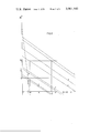
- the output voltage signal (IST4) at the output terminal (31) as well as the voltage signals at the base of transistor T7 (BST7), the collector of transistor T10 (cT10), the reference voltages VZ31, VZ8 and the threshold voltage values Tr1 and Tr4 are represented in function of time t on FIG. 4.
- the transistor T7 (FIG. 2) remains conductive during the time interval determined by the instants separating the signal peaks above Tr4.
- Transistor T10 remains now saturated during the time interval T7 is conductive. Due to the above the following happens:
- Transistor T11 in the detection circuit DET21 (FIG. 2) is blocked since its base voltage is maintained at the Zener reference voltage (VZ31) via the clamping diode D37;
- the resistor R31 in the signal output circuit SI1 is switched through i.e. connected to the above Zener reference voltage VZ31 via the diode D25 and conductive transistor T10;
- Transistor T13 and consequently transistor T24 both become conductive;
- the part of the signal output circuit SI1 including the transistors T10, T13, T24 is isolated from the rest of the signal output circuit of the individual receiver IR1 by means of the diode D22 since the collector of transistor T7 is now fed from battery via diode D19, resistor R24 and conductive transistor T22 (FIG. 3);
- Transistors T10 and T24 are maintained conductive since their bases are supplied with base current via transistor T13 and resistors R28 and R43 respectively;
- the tank circuit F11 is short-circuited by means of the diode D71 (FIG. 2) connected to battery via the conductive transistor T22 thus preventing the individual receivers IR1 and IR2 from reacting to disturbing signals as explained below.
- This short-circuiting has no effect on the state of the transistor T10, T13 and T24 in the signal output circuit SI1 and on the evaluation circuit EV since the transistors T10, T13 and T24 and T22, T23 in EV are maintained conductive.
- An output signal is now provided at the output terminals OUT1 and OUT2 (not shown) of the individual receivers IR1 and IR2 (not shown). These signals may be recognized by the computer (not shown). When this has taken place backward signals are sent to the signal generator means until these backward signals are recognized. The generator means then stops the emission of forward signals so that transistor T15 (FIG. 3) becomes blocked. As a consequence thereof transistor T16 (FIG. 3) in the 2 out of 5 check circuit becomes conductive whereby finally transistors T22 and T23 both are blocked and the tank circuits F11 and F12 are no longer short-circuited. Consequently, transistors T13, T10 and T24 (FIG. 2) become blocked and the system is ready for the reception of the following new frequency code.
- the curves 3', 4', 5' and 3" will be referred to later.
- the envelopes 1, 2, 3, 3', 4, 4', 5, 5' are parallel straight lines the necessity of which will become clear below. It is known that a resonant circuit will continue to oscillate when an input signal fed to this circuit is stopped.
- the amplitude of the oscillations will decay exponentially with a time constant which is proportional to the ratio of the quality factor Q and the tuned frequency f and this phenomenon is independent of the nature of the input signal. This may f.i. be the case when a noise signal in the form of projects, contact interruptions, short or long noise bursts etc arrive at the input terminal IN of the system and cease suddenly.
- the total threshold voltage Tr1 is the sum of this cut-in voltage and the voltage developed across the resistance capacitance network R'34, C10 which is due to the rectified output signal at the output terminal (21) of tank circuit F11 (FIG. 2). Since also the tapping point (41) delivers an output signal which is larger than that at the tapping point (21) the transistor T11 will become conductive for a certain value of the output signal at the tapping point (41).
- the above cut-in voltage value can partially or totally be compensated by having the junction point of the resistors R'23 and R34 connected to a point the voltage of which is below the reference voltage value VZ8.
- the threshold voltage is proportional to the voltage value of the output signal at the output terminal (21) and consequently also to the input signal at the input terminal (11) of the tuned circuit F11. This is a necessary measure since when the threshold voltage value would remain constant the bandwidth at this voltage value of the tuned circuit F11 would increase with an increasing input signal.
- transistor T8 is conductive since its emitter and base are connected to battery via resistor R'19 and to the junction point of the resistors R'23 and R21 of the potentiometer circuit R'23, R21, R20 via resistor R23 respectively. Due to the voltage drop across the resistor R'23 the emitter voltage of the emitter follower T8 is below the reference voltage VZ8. Secondly, the voltage at the emitter of transistor T9 is held at a higher potential than that of its base by the clamping diode D6. Consequently transistor T9 is blocked. Transistor T'10 is conductive since its emitter is connected to battery via resistor R14. This emitter voltage will thus remain constant as long as transistor T9 is blocked.
- transistor T9 becomes conductive due to the base voltage of transistor T8 having been sufficiently increased, the emitter voltage of transistor T'10 increases beyond the above mentioned constant voltage.
- the transistor T1 wherein base current flows via resistors R29, R'28, R27 and R26 is conductive.
- the capacitor C11 is thus charged at its emitter voltage which is smaller than the emitter voltage of transistor T8.
- a pulse applied at the base of transistor T8 will momentarily increase the base current in transistor T1 via diode D3, capacitors C8 and C11 whereby the charge and consequently the voltage across the latter capacitor increases.
- the operation of the threshold circuit THR4 will first be considered under steady state conditions i.e. when a normal signal having a frequency f1 is received. A DC voltage is then applied at the base of transistor T8 due to the action of rectifying circuit Re21 (FIG. 2) and the resistance capacitance filter network C9, R23 (FIG. 3). At the same time an output signal from the output terminal (31) is applied to the base of transistor T41 of the detection circuit DET11 (FIG. 2). When the voltage of this output signal increases above the earlier mentioned constant voltage at the emitter of transistor T'10, transistor T41 is rendered conductive. When the voltage of the output signal has increased above this constant voltage by a certain amount, transistor T9 becomes conductive due to the base voltage at transistor T8 having been sufficiently increased. From that moment on the threshold voltage value Tr4 increases with the output signal at the output terminal (31) and consequently also with input signal
Landscapes
- Engineering & Computer Science (AREA)
- Computer Networks & Wireless Communication (AREA)
- Monitoring And Testing Of Transmission In General (AREA)
- Networks Using Active Elements (AREA)
- Stereo-Broadcasting Methods (AREA)
- Laying Of Electric Cables Or Lines Outside (AREA)
- Tone Control, Compression And Expansion, Limiting Amplitude (AREA)
- Noise Elimination (AREA)
Applications Claiming Priority (2)
| Application Number | Priority Date | Filing Date | Title |
|---|---|---|---|
| NL7312548A NL7312548A (nl) | 1973-09-12 | 1973-09-12 | Multifrequent signaleringsstelsel. |
| NL7312548 | 1973-09-12 |
Publications (1)
| Publication Number | Publication Date |
|---|---|
| US3961143A true US3961143A (en) | 1976-06-01 |
Family
ID=19819583
Family Applications (1)
| Application Number | Title | Priority Date | Filing Date |
|---|---|---|---|
| US05/505,014 Expired - Lifetime US3961143A (en) | 1973-09-12 | 1974-09-11 | Multi-frequency signalling system |
Country Status (12)
| Country | Link |
|---|---|
| US (1) | US3961143A (fr) |
| BE (1) | BE819816A (fr) |
| BR (1) | BR7407544A (fr) |
| DE (1) | DE2442674A1 (fr) |
| ES (1) | ES429974A1 (fr) |
| FR (1) | FR2243572B1 (fr) |
| GB (1) | GB1474403A (fr) |
| IE (1) | IE40288B1 (fr) |
| IT (1) | IT1021273B (fr) |
| NL (1) | NL7312548A (fr) |
| NO (1) | NO140727C (fr) |
| ZA (1) | ZA744657B (fr) |
Cited By (5)
| Publication number | Priority date | Publication date | Assignee | Title |
|---|---|---|---|---|
| FR2399175A1 (fr) * | 1977-07-26 | 1979-02-23 | Western Electric Co | Dispositif de detection de la reception de signaux multifrequence |
| US4145580A (en) * | 1977-01-24 | 1979-03-20 | Nippon Electric Co., Ltd. | Multi-frequency signal receiver |
| DE3015567A1 (de) * | 1979-04-27 | 1980-11-13 | Int Standard Electric Corp | Digitales signalisierungssystem, insbesondere fuer fernsprechanlagen |
| US5170487A (en) * | 1989-01-19 | 1992-12-08 | Seiko Corp. | Paging system with multiple frequencies and multiple protocols |
| US20060030267A1 (en) * | 2004-03-29 | 2006-02-09 | Engim, Inc. | Detecting and eliminating spurious energy in communications systems via multi-channel processing |
Citations (3)
| Publication number | Priority date | Publication date | Assignee | Title |
|---|---|---|---|---|
| US3072747A (en) * | 1958-05-27 | 1963-01-08 | Ass Elect Ind Woolwich Ltd | Pulse signalling systems |
| US3128349A (en) * | 1960-08-22 | 1964-04-07 | Bell Telephone Labor Inc | Multifrequency signal receiver |
| US3539731A (en) * | 1968-11-05 | 1970-11-10 | Bell Telephone Labor Inc | Multifrequency signal receiver |
-
1973
- 1973-09-12 NL NL7312548A patent/NL7312548A/xx not_active Application Discontinuation
-
1974
- 1974-07-11 GB GB3069774A patent/GB1474403A/en not_active Expired
- 1974-07-22 ZA ZA00744657A patent/ZA744657B/xx unknown
- 1974-07-23 IE IE1569/74A patent/IE40288B1/en unknown
- 1974-09-05 NO NO743189A patent/NO140727C/no unknown
- 1974-09-06 DE DE2442674A patent/DE2442674A1/de not_active Withdrawn
- 1974-09-11 FR FR7430733A patent/FR2243572B1/fr not_active Expired
- 1974-09-11 IT IT27163/74A patent/IT1021273B/it active
- 1974-09-11 BR BR7544/74A patent/BR7407544A/pt unknown
- 1974-09-11 US US05/505,014 patent/US3961143A/en not_active Expired - Lifetime
- 1974-09-11 ES ES429974A patent/ES429974A1/es not_active Expired
- 1974-09-12 BE BE2053860A patent/BE819816A/xx not_active IP Right Cessation
Patent Citations (3)
| Publication number | Priority date | Publication date | Assignee | Title |
|---|---|---|---|---|
| US3072747A (en) * | 1958-05-27 | 1963-01-08 | Ass Elect Ind Woolwich Ltd | Pulse signalling systems |
| US3128349A (en) * | 1960-08-22 | 1964-04-07 | Bell Telephone Labor Inc | Multifrequency signal receiver |
| US3539731A (en) * | 1968-11-05 | 1970-11-10 | Bell Telephone Labor Inc | Multifrequency signal receiver |
Cited By (7)
| Publication number | Priority date | Publication date | Assignee | Title |
|---|---|---|---|---|
| US4145580A (en) * | 1977-01-24 | 1979-03-20 | Nippon Electric Co., Ltd. | Multi-frequency signal receiver |
| FR2399175A1 (fr) * | 1977-07-26 | 1979-02-23 | Western Electric Co | Dispositif de detection de la reception de signaux multifrequence |
| DE3015567A1 (de) * | 1979-04-27 | 1980-11-13 | Int Standard Electric Corp | Digitales signalisierungssystem, insbesondere fuer fernsprechanlagen |
| DE3015567C2 (de) * | 1979-04-27 | 1986-09-11 | International Standard Electric Corp., New York, N.Y. | Digitaler Mehrfrequenzcodeempfänger mit Störschutzschaltungen in Fernmelde-, insbesondere Fernsprechanlagen |
| US5170487A (en) * | 1989-01-19 | 1992-12-08 | Seiko Corp. | Paging system with multiple frequencies and multiple protocols |
| US20060030267A1 (en) * | 2004-03-29 | 2006-02-09 | Engim, Inc. | Detecting and eliminating spurious energy in communications systems via multi-channel processing |
| US7835701B2 (en) * | 2004-03-29 | 2010-11-16 | Edgewater Computer Systems, Inc. | Detecting and eliminating spurious energy in communications systems via multi-channel processing |
Also Published As
| Publication number | Publication date |
|---|---|
| GB1474403A (en) | 1977-05-25 |
| IE40288B1 (en) | 1979-04-25 |
| BR7407544A (pt) | 1976-05-04 |
| ZA744657B (en) | 1975-08-27 |
| FR2243572B1 (fr) | 1978-02-17 |
| NO140727C (no) | 1979-10-24 |
| DE2442674A1 (de) | 1975-03-13 |
| FR2243572A1 (fr) | 1975-04-04 |
| IE40288L (en) | 1975-03-12 |
| AU7177174A (en) | 1976-01-29 |
| BE819816A (nl) | 1975-03-12 |
| ES429974A1 (es) | 1976-10-01 |
| NL7312548A (nl) | 1975-03-14 |
| NO743189L (fr) | 1975-04-07 |
| NO140727B (no) | 1979-07-16 |
| IT1021273B (it) | 1978-01-30 |
Similar Documents
| Publication | Publication Date | Title |
|---|---|---|
| US5994689A (en) | Photoelectric cell with stabilised amplification | |
| US3821484A (en) | Time sharing of a supervisory receiver unit | |
| US3868639A (en) | Remote control receiver responsive to sound | |
| JPS635932B2 (fr) | ||
| US3961143A (en) | Multi-frequency signalling system | |
| US2935572A (en) | Electrical signaling system | |
| US3710031A (en) | Multi frequency receiver | |
| US4198620A (en) | Remote control receiver | |
| US2880331A (en) | Time controlled signal discriminator circuit | |
| US3936617A (en) | Code-controlled ringer attachment for telephones | |
| US3140445A (en) | Communication receiver with noise blanking | |
| US3539731A (en) | Multifrequency signal receiver | |
| US3393274A (en) | Subscriber loop and trunk loop range extension circuit | |
| US4042790A (en) | Voice guard circuit for a tone receiver | |
| US2957950A (en) | Transistor selective ringing circuit | |
| US3602821A (en) | Noise immune pure carrier detector circuit | |
| US4042789A (en) | Tone combination detector and coincidence timer circuit | |
| US3165699A (en) | Automatic gain control system for suppressed carrier single sideband radio receivers | |
| US3184716A (en) | Guarded tone signalling | |
| US2939950A (en) | Combined manual and automatic gain control circuit | |
| GB1377021A (en) | Signal receiver for receiving signals of different frequency | |
| US4129886A (en) | Digital remote control system | |
| US3319011A (en) | Multifrequency signal receiver circuit | |
| US3078444A (en) | Remote control system | |
| US4004105A (en) | Multifrequency signal receiver for use in telephone signaling systems or the like |
Legal Events
| Date | Code | Title | Description |
|---|---|---|---|
| AS | Assignment |
Owner name: ALCATEL N.V., DE LAIRESSESTRAAT 153, 1075 HK AMSTE Free format text: ASSIGNMENT OF ASSIGNORS INTEREST.;ASSIGNOR:INTERNATIONAL STANDARD ELECTRIC CORPORATION, A CORP OF DE;REEL/FRAME:004718/0023 Effective date: 19870311 |