US3763473A - Multiport data storage transfer system - Google Patents
Multiport data storage transfer system Download PDFInfo
- Publication number
- US3763473A US3763473A US00159982A US3763473DA US3763473A US 3763473 A US3763473 A US 3763473A US 00159982 A US00159982 A US 00159982A US 3763473D A US3763473D A US 3763473DA US 3763473 A US3763473 A US 3763473A
- Authority
- US
- United States
- Prior art keywords
- data
- storage
- transfer
- sensing
- interconnecting
- Prior art date
- Legal status (The legal status is an assumption and is not a legal conclusion. Google has not performed a legal analysis and makes no representation as to the accuracy of the status listed.)
- Expired - Lifetime
Links
Images


Classifications
-
- G—PHYSICS
- G06—COMPUTING OR CALCULATING; COUNTING
- G06F—ELECTRIC DIGITAL DATA PROCESSING
- G06F13/00—Interconnection of, or transfer of information or other signals between, memories, input/output devices or central processing units
- G06F13/10—Program control for peripheral devices
- G06F13/12—Program control for peripheral devices using hardware independent of the central processor, e.g. channel or peripheral processor
- G06F13/122—Program control for peripheral devices using hardware independent of the central processor, e.g. channel or peripheral processor where hardware performs an I/O function other than control of data transfer
Definitions
- ABSTRACT A storage device to serve as a temporary or buffer storage includes a plurality of different memory locations, data entering and data sensing devices and associated equipment permitting the individual and independent addressing of each storage location.
- a first set of switching circuits interrelate certain data entering and data reading devices with the storage device and a further set of switching circuits interrelate other groups of data entering and reading devices to the storage device, all of which switching circuits are individually controllable such that the associated entering and reading devices can be individually and independently placed in an active state at different or the same times.
- Individual terminals or ports are also provided interconnecting the various switching circuits with peripheral equipment, e.g., CRT displays, magnetic tape, and data processing equipment.
- Present known systems solve concurrent requests for data transfer by timesharing transfer channels which requires channel switching means, program instructions to control the switching means for storing program instruction and control for the storage locations.
- all operational steps have to be coordinated by the system.
- Hardware and software for these known systems represent a very complex arrangement which is difficult to set-up and requires personnel having good knowledge of the system as well as an exceptionally high level of skill to make any change in or upgrade an existing system.
- the two general methods of data entry presently used are entry via keyboard onto punched or magnetic tape or punched cards and entry directly into a processor using timesharing techniques. Both approaches use temporary storage: in the first case, the tape or cards, and in the second case, the processor main frame memory. In either case, the time for throughput of data and report generation, as well as equipment cost and complexity of programming, leave much to be desired. Specifically, in connection with data entry devices that utilize a data processor main frame memory for temporary storage, this interrupts the processor operation, occupies valuable storage space and requires programming to handle the data entry and verification, all of which add to the ultimate expense of the system.
- a further object is the provision of a system as in the above objects in which simultaneous random access is available to any or all of a plurality of difierent storage locations.
- Another object is a simplified system having multiple independent data transfer paths between the storage locations and associated equipment.
- a still further object is provision of a system not requiring program control for simultaneous transfer between storage areas and associated equipment.
- Yet another object is the provision of a system as described in the preceding objects offering optimal flexibility in selection of the kind, number and arrangement of data input/output and handling equipment.
- a data storage transfer system having a main memory serving as a temporary or buffer storage which includes a plurality of different memory locations, and associated equipment permitting the individual and independent addressing of the locations.
- a first set of switching means interrelate certain data entering and data reading devices with the main memory.
- a further set of switching means interrelate other groups of data entering and reading devices. All of the switching means are individually controllable such that the associated entering and reading devices can be individually and independently placed in an active state at different or the same times.
- Means are also provided interconnecting the various switching means with peripheral equipment, e.g., CRT displays, magnetic tape, and data processing equipment.
- FIG. 1 is a schematic depiction of different kinds of auxiliary or peripheral euipment interrelated with the storage transfer system of this invention.
- FIG. 2 is a schematic function block diagram of the major elements of the system of this invention.
- FIG. 3 is a stylized depiction of the system showing utilization of a drum memory as the main frame memory.
- FIG. 4 is a perspective view of a drum memory for use in the system of FIG. 3.
- FIG. 5 is a schematic representation of the overall system depicting generalized data flow therethrough.
- FIG. 6 is a function block circuit diagram of one form of switching means for use in the described system.
- FIG. 7 is a schematic representation of an arrangement for synchronizing rotating memories.
- the system of this invention is shown interconnected with a number of different kinds of auxiliary or peripheral equipment. It is to be understood that the number and kind of such peripheral equipment shown in the drawing and described herein are merely illustrative and are not intended to be limitative in this regard.
- the storage transfer system of the invention is generally enumerated as at 10 and more particularly identified as Multiport Data Storage and Transfer System.
- the peripheral equipment interconnected with the system, and thereby interrelated to one another, may include a data processor 11, magnetic tape files 12, a line printer 13, a pair of cathode ray display units 14 and 15, a character printer or typewriter l6 and a data link such as a telephone system or socalled modem 17.
- the various peripheral equipment items are provided buffer storage and transfer channels by and between each other either on a simultaneous or time spaced manner through the storage transfer system 10. That is, a plurality of different operations can be simultaneously accomplished with data read into and out of the main memory of the system I0 and all at the same time without recourse to time sharing being necessary.
- FIG. 1 The various interfacing ports for the different peripheral equipment items are further identified in FIG. 1 by the letters A. B. C.
- port A which has accessibility to all system storage areas requiring communication.
- the data processor I1 is handled by port B, the magnetic tape apparatus 12 by port C, and so forth for all the peripherals.
- FIG. 2 there is shown there a basic block diagram of an arrangement using a multiport memory or data transfer storage 18 as a data buffer or temporary storage means interconnected with various external equipment.
- a data file 19 is a memory, such as a magnetic disk file for example, which stores all data and program information necessary for controlling data storage 18 and the data processor 20.
- Program information is transferred to the data processing control 22 directly from 19 whereas data is exchanged from the file 19 through data transfer storage 18 with peripheral equipment via the input/output (IIO) channels 23 and a further storage means termed the working file storage 24.
- the data processor can exchange data with any of the devices connected via the IIO channel 23 and with the working file storage 24 through data transfer storage 18.
- the data processor 20 is controlled by data processing control 22 with all transfers through data transfer storage 18 being under the supervision of data transfer control 21.
- FIG. 2 The arrangement of FIG. 2 described immediately above provides one set of independent storage locations in the storage 18 for each peripheral device connected through the channels 23, and several sets of independent storage locations for the data processor 20 to separate data to be processed from that data already processed.
- Other storage locations in 18 operate as temporary storage during data transfer from and to the data file 19.
- each of the storage locations in the data transfer storage 18 can be read into or out of independently of all the other locations, thereby providing for simultaneous access to a pluraity of different storage locations not requiring the multiplex techniques used in certain prior systems or complex programming involved in certain other system.
- FIG. 3 illustrates in somewhat more detail the system of this invention utilizing a rotating magnetic drum memory 25 as the data transfer storage 18.
- the drum memory includes a cylindrical body having a magnetizable coating on its circumferential periphery.
- a plurality of signal recording and sensing heads 26-33 are fixedly mounted closely adjacent the magnetizable surface of the drum, with each head operating on a single circular track of the drum periphery as the drum is rotated about its axis 34.
- the drum recording surface has portions defining a single track with an associated data entering and data sensing head associated therewith, and other common function portions defined by a plurality of tracks and heads.
- all recording and sensing heads assigned to the same transfer path are controlled by the same sensing and recording circuit apparatus which includes a plurality of selectively actuatable head switching means.
- the signal head switching circuit apparatus selects at any one time only one signal head within its group, but any particular signal head is selectable by more than one signal switching apparatus.
- Each head is connected to a separate switching means 36-45, with it to be understood that the number of heads and associated switching means have merely been chosen for purposes of explanation and in actuality many more such heads and switching means are required.
- the letters R and R/W have been used to designate the function of the controlled heads as rea or sensing and read/write" or sensing and data entering, respectively.
- Drum storage band 47, 48, 49 and 50 can receive and read out data stored therein through switching means 37 through 40 to access ports 51, 52, 53 and 54 respectively under control of the storage read/write control 47.
- switching means 44 interrelate port 58 with storage bands 47, 48, 49, S0, 55 and 56. This capability is additionally referenced on the drawing as multiple storage access arrangements.
- the transfer switching means 59 and 60 provide for inter and intra storage data transfer. That is, not only can new information be introduced from peripheral equipment for storage, but by suitable actuation of the switching means 59 and 60, information can be read out of any storage track/s in bands 46-50 and recorded into any other track on the drum. It is important to note that transfer of information from one track or one location on the drum to another can be performed independently of what is occurring at any of the other signal recording and sensing heads.
- Program information for the data processor 61 is read out of the program band 56 through the switching means 43. Heads 31 and 32 are provided to supply to and sink data from the processor.
- Each of the switching means 36-45, 59 and 60 are provided with enabling signals a, b, m at respectively different times to insure that no sensing or recording head is activated by two or more switching means at the same time.
- FIG. 4 there is shown a typical drum memory for use as the buffer storage medium described above in connection with the system of FIG. 3.
- a memory for satisfactory operation in the subject system must include a sufficient number of sensing and recording heads suitably spaced from one another about the recording surface as to insure freedom from crosstalk.
- a base plate 62 is mounted on shock and vibration absorbers 63 to provide isolation of the spinning drum 64 from external mechanical interference.
- L-shaped mounting members 65 are affixed to the upper surface of the base plate 62 for carrying heads 66 suitably positioned to sense and record on the circumferential periphery 67 which is provided with a magnetizable recording coating.
- a rotative power source 68 drives the drum 64 about its axis 69 at a relatively high velocity, e.g., 3,600 rpm or more.
- FIG. 5 there is shown operation of the present invention primarily in connection with the use of dedicated storage data.
- a circle has been used to represent a storage band consisting of one or more drum tracks, and sensing and recording heads are depicted as separate entities although typically both functions can be accomplished in a single head appropriately connected to both recording and sense amplifiers.
- FIG. 5 circuit Basic control for the FIG. 5 circuit is maintained by storage control 70 which has the dedicated storage band 46 of FIG. 3 for temporary storage use.
- the program storage receives program information from any one of the disk file storage units 71-73 through the file select control 74, file input/output control 75 and distributor DMX 76. Except for initial set up, all of the equipment switching information from one storage location to another is dependent upon the program unit control 70.
- the unit 70 is also responsive to command signals or request input a and b as shown and can issue all control signals essential for any proposed data transfer.
- peripheral controller 79 controls CRT display 14 and a printer 13; and controller 80 controls a magnetic tape unit 12 and a CRT display 15.
- the peripherals 12 to 15 are merely exemplary and it is to be understood that the described equipment can accommodate other and different peripherals as well.
- data information may be stored in the set of storage locations 83 or 84 from which data can be transferred under the control of the program unit 70 to disk storages 71-73.
- the set of locations 83 and 84 are selected tracks within a band such as 48 (FIG. 3) and operate as input temporary or buffer storage.
- Data transfer from disk file storages 71-73 to a pcripheral is accomplished via file select 74, [/0 control 75, distributor 76, and controls 85 and 86 to temporarily store in the set of drum tracks 87 and 88.
- Transfer of data from tracks 87 and 88 to peripheral displays 12-15 is through multiplexers 89 and 90, respectively, and distributors 79 and 80.
- Each of the circuit means 74-76, 79, 80, 89 and 90 are bidirectional switching means which perform a data selection function for one transfer direction and as distributors for transfers in the opposite direction.
- FIG. 5 can be expanded by adding more ports, each having input and output buffer storage tracks and interconnected with the remainder of the system through a separate port.
- accessibility is controlled by the switching means 92 and 93, the latter being further identified as 0 (output) and I (input), respectively.
- Any one of the four storage bands of 91 can receive data from or store data in any disk storage 71-73.
- any of the storage bands in 91 can store data in the tracks 87 and 88 for subsequent transfer to a peripheral.
- disk storage 91 can write into drum bands 94 and read out of bands 95.
- the sets of storage tracks 94 and 95 serve as input and output, respectively, for the processor 61, the stored control program for which is contained in tracks 96.
- the working storage 91 serves as temporary storage for input and output to the processor.
- data from one or more of the files 71-73 are transferred to working storage 91 and also to the processor 61. Until processing is complete, no further transfer of data from files 71-73 occurs which makes them available to the other peripherals during time of data processing.
- Instant updating of data entered at one of the peripherals is provided via controls 83, 84, 97 and 98.
- the CRT displays 14 and 15 can be made to instantly indicate any change of data entered via, say, a character printer 16 or phone link 17 (FIG. 1).
- FIG. 5 is a schematic diagram includes synchronizing means 122 for synchronoualy transferring data between drum storage tracks 46, 83, 84, 87, 88, 94, 95, and 96 and any of the file storages 71, 72, 73. Synchronous transfer of data simplifies the hardware required to interface these rotating memories, and increases efficiency of the system by reducing the time required for data transfer.
- Synchronizing means 122 receive signals from drum drive 120 and from the drives of disk storages 71, 72 and 73. By its repetition rate, each signal indicates the rate of rotation of the particular storage device. The time between the occurrence of each signal indicates the time required for the completion of each rotation. Comparison of the repetition rate of the signals from a disk drive (such as 71-73) and drum drive 120 results in an output signal which will keep the relative rates of rotation of the disk drive and drum drive at a fixed ratio with respect to each other. Therefore, after reaching the speed synchronization, a comparison of the time of occurrence of each signal is used to force the disk drive into a fixed angular position relative to the drum drive.
- a disk storage rotating in synchronization and phase lock with the drum storage performs its functions as if the disk storage were an integral part of the drum storage area. Similar methods (not shown) are used to interface the drum and other peripherals which are capable of operating at the bit rate of the drum storage of the system.
- the synchronizing means is able to individually synchronize such memories to coordinate the transfer of data.
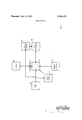
- FIG. 6 shows one form of circuit apparatus for use in this connection.
- the apparatus shown there includes four AND-gates 99-102, a further set of four AND-gates 103-106 and an OR-gate 107, all of which cooperate to provide bidirectional flow of data from any of the four channels A, B, C, or D with respect to the main channel including leads 108 and 109.
- the direction of data flow is indicated in the drawing by arrows located adjacent each of the various leads.
- Data provided on lead 108 serves as an input to each of the AND-gates 99-102, the respective output from which AND-gates is fed individually into channels A, B, C and D.
- AND-gates 99-102 are all provided with enabling signals via lead 110 which is a general signal to effect transfer to the lettered channels. Further, individual select signals are provided via leads 111-114 to each of the same AND-gates. Therefore, to provide information from main channel lead 108 to, say, channel A, not only must there be a signal on lead 108, but it must be concurrent with an up condition on 110 and 111.
- signals from each of the AND-gates 103-106 are activated by channels A, B, C and D as well as appropriate channel select signals and a common input gating pulse on lead 115, the latter generally commanding a transfer to the main channel. Since any of the information being gated via 103-106 is to be sent onto a single lead 109, the outputs of AND-gated 103-106 are OR-gated via 107.
- any signals present on main channel lead 108 may be selectively fed into any one or collection of channels A, B, C or D by merely energizing the appropriate channel select lead. That is, a multiplexing is achieved in that the signals on 108 can be fed out onto any one or all of four different channels. As to incoming signals on the channels A, B, C and D, these are demultiplexed via AND- gates 103-106 and OR-gate 107 to appear on the single main channel lead 109.
- the speed and phase synchronization of disk and drum rotation is achieved by comparing signals which are generated at the devices which are to be synchronized. More particularly, a signal indicating the speed and phase condition of the drum drive is supplied to synchronizing means 122 via the line 123 (FIG. 7). This signal is in the form of a series of pulses which are fed to a pulse shaper 124. Shaper 124 generates uniform pulses which are integrated in integrator 125. The output signal of the integrator 125 is a dc signal having a voltage level which is proportional, in voltage, to the speed of the drum storage.
- a corresponding pulse signal from a drive associated with one of the disk storages 71, 72, 73 is supplied to the arrangement of FIG. 7 via the line 127.
- the pulses constituting this signal enter a pulse shaper 128 and are fed from shaper 128 to integrator 129.
- the dc output signal of integrator 129 has a voltage level which is proportional to the speed of the particular disk drive. Both of these dc signals are supplied from integrator 125 and from integrator 129 to a comparator 126. Responsive thereto, an output signal appears on line 135 with a magnitude which is proportional to the voltage level difference between the input signals.
- a signal appears on line 130 when there is a match between the voltage levels of both input signals (within a given limit).
- the differential output signal on line is fed directly into a controlled power supply 136, of the particular disk drive.
- the output power of of supply 136 increases or decreases the power to the disk drive via the line 137 to increase of decrease the drive speed.
- Signals from the pulse shapers 124 and 128 are fed via lines 131 and 132, respectively, into a coincidence circuit 133.
- This coincidence circuit 133 receives an enable signal as soon as both devices (the drum drive 120 and the particular disk drive) reach speed synchronism.
- Circuit 133 compares the time of occurrence of the two signal pulses and generates an output pulse on line 134. The magnitude of the generated pulse is proportional to the interval between the occurrence of a pulse on line 131 and a pulse on line 132.
- These output pulses on line 134 induce the power supply 136 to issue short power pulses on line 137, in addition to the average output level caused by signals on line 135.
- these short power pulses momentarily increase or decrease the speed of the disk drive.
- the time intervals between the disk and drum pulses appearing on lines 123, 127 are controlled until the deviation from normal is reduced to zero.
- a coincidence between the pulse signals from drum drive 120 and a particular disk drive indicates an in-phase operation of both devices.
- the output lines 138 and 139 provide for connections between the drum drive and other circuitry (similar to the described arrangement of FIG. 7) for controlling other disk drives.
- FIG. 7 can also be implemented using either linear signal processing means or digital signal processing means.
- each storage area When disk storage is used, each operates at its own uncontrolled speed.
- the peripheral device serviced by each storage area supplies the pulse signals required for synchronization via wire 127.
- the cyclically operating storage means provides speed reference signals on wire 123.
- the synchronizing signals on wire 137 may also control other storage devices such as shift registers, delay lines, and cyclically operated random access memories.
- gating circuits such as shown in the bottom half of FIG. 6 may be used. Gates of this type (called multiplexers”) are readily available on the open market and sometimes designated as type 9309 or 93 I2, preferably made by the Fairchild Company.
- a storage system for storing data comprising, in combination:
- data storage means having a plurality of storage areas for storing data
- each access means being individually associated with a dedicated one of said storage areas;
- a plurality of selectively actuatable first switching circuit means interconnecting each of said plurality of dedicated storage area access means with each of said transfer means for effecting concurrent transfer of data between storage areas and data entering and utilization means;
- At least one selectively actuatable second switching circuit means interconnecting more than one of said plurality of said dedicated storage area access means with one of said plurality of transfer means;
- central control means for selectively actuating and individually operating any of said first and second switching means to transfer data from said dedicated areas to said data entering and utilizing means.
- a storage system as claimed in claim I wherein certain of said transfer means include intermediate storage means for storing data; first circuit means interconnecting one of said first and second switching fer rate during transfers of data between said intermediate storage means and said first switching means; said second circuit means operating at a second transfer rate during transfers of data between said intermediate storage means and said data entering and data utilization means; said intermediate storage means adapted to operate selectively at said first and said second transfer rate.
- Data transfer apparatus comprising:
- first circuit means interconnecting certain of said terminals with certain data storing and sensing means
- second switching circuit means interconnecting at least one of said terminals with at least two of said data storing and sensing means
- Data transfer apparatus as in claim 6 and the data processing means coupled to said data storage means for processing said stored data.
- Data transfer apparatus as in claim 7 and data phone means also coupled to said data storage means for transmitting said stored data to a distant location.
- one of said data utilization devices includes a cathode ray tube; and means interconnected therewith for providing a repetitive display of data being entered, stored, and sensed in a given group of storage locations.
- said selectively actuatable switching means include a plurality of movable mechanical supports each carrying one of said data storing and sensing means; and means for controlling the movement of each of said supports to bring said storing and sensing means in operative proximity with a prescribed storage area of said storage.
- a data transfer system for accommodating a plurality of different types of data generating and data utilizing peripheral equipments, each type of equipment having its own distinctive input/output characteristics comprising:
- means associated with said storage means for storing and sensing data in said storage means including means for sensing data in each location, means for recording data in each location;
- each terminal serving as a data port for a particular type of associated peripheral equipment
- first switching circuit means interconnecting at least one of said terminal means and the recording and sensing means of a buffer storage means for thereafter providing selective access to transfer the data between said buffer storage means and any storage location in said storage means;
- second switching circuit means interconnecting other terminal means to predetermined groups of storage locations in said storage means
- third switching circuit means interconnecting certain of said sensing means with certain of said recording means, whereby data sensed by said certain sensing means are stored elsewhere in the storage means via said certain recording means;
- a storage system for storing data comprising in combination:
- a cyclically operated data storage means having a plurality of individually effective storage areas for storing data
- a plurality of controlled first switching circuit means interconnecting certain of said plurality of said storage area access means with certain of said transfer means for concurrent transfer of data between different storage areas and different data entering and data utilization means;
- At least one controlled second switching circuit means interconnecting more than one of said plurality of storage area access means with one of said plurality of transfer means;
- a storage system for storing data as claimed in claim 16 including controlled third switching circuit means interconnecting certain of said plurality of data storage area access means with certain other of said data storage area access means;
- Data transfer apparatus comprising: a plurality of peripheral data input devices having different language" characteristics;
- first circuit means interconnecting certain of said first terminals with certain data storing and sensing means
- second circuit means interconnecting at least one of said second terminals with at least two of said data storing and sensing means.
- Data transfer apparatus as in claim 19, in which one of said data utilization devices includes a cathode ray tube; and means are interconnected therewith for providing a repetitive display of data being entered and data being sensed in a given group of storage locations.
- first circuit means interconnecting one of said first and second switching means with said intermediate storage means
- first circuit means operating at a first transfer rate during transfers of data between said intermediate storage means and said first switching means; said second circuit means operating at a second transfer rate during transfers of data between said intermediate storage means and said data entering or utilization means; said intermediate storage means adapted to operate selectively at said first and said second transfer rate.
- a data transfer system for accommodating a plurality of different types of data generating and data utilizing peripheral equipment comprising:
- data storage means having a plurality of different storage locations dedicated to said equipment according to the types thereof;
- means for sensing data in each dedicated location means for recording data in each dedicated location;
- first switching circuit means interconnecting at least one of said terminal means and the recording and sensing means providing selective access to any storage location in said storage means;
- second switching circuit means interconnecting other terminal means to predetermined groups of storage locations in said storage means
- third switching circuit means interconnecting said means for sensing data with said means for recording data, whereby data sensed by said means for sensing data are directly stored elsewhere in said storage means;
- a storage transfer system as in claim 24 in which at least certain of said peripheral equipment have different data generating and data utilizing rates from said other peripheral equipment.
- a front-end data transfer apparatus for a computer comprising in combination:
- first data storage means for storing data having a plurality of storage locations
- fourth and fifth data port said fourth data port connected to one or more of said storage locations, said fifth data port interconnecting said fourth data port with others of said storage locations for transfer of data from one of said storage locations to another one;
- control means for controlling said first to fifth ports.
Landscapes
- Engineering & Computer Science (AREA)
- Theoretical Computer Science (AREA)
- Physics & Mathematics (AREA)
- General Engineering & Computer Science (AREA)
- General Physics & Mathematics (AREA)
- Signal Processing For Digital Recording And Reproducing (AREA)
- Multi Processors (AREA)
- Information Transfer Systems (AREA)
Applications Claiming Priority (1)
| Application Number | Priority Date | Filing Date | Title |
|---|---|---|---|
| US15998271A | 1971-07-06 | 1971-07-06 |
Publications (1)
| Publication Number | Publication Date |
|---|---|
| US3763473A true US3763473A (en) | 1973-10-02 |
Family
ID=22574964
Family Applications (1)
| Application Number | Title | Priority Date | Filing Date |
|---|---|---|---|
| US00159982A Expired - Lifetime US3763473A (en) | 1971-07-06 | 1971-07-06 | Multiport data storage transfer system |
Country Status (5)
| Country | Link |
|---|---|
| US (1) | US3763473A (oth) |
| JP (1) | JPS548268B1 (oth) |
| DE (1) | DE2233270A1 (oth) |
| FR (1) | FR2145252A5 (oth) |
| GB (1) | GB1400487A (oth) |
Cited By (1)
| Publication number | Priority date | Publication date | Assignee | Title |
|---|---|---|---|---|
| USRE31790E (en) * | 1974-03-13 | 1985-01-01 | Sperry Corporation | Shared processor data entry system |
Families Citing this family (1)
| Publication number | Priority date | Publication date | Assignee | Title |
|---|---|---|---|---|
| CN103678171A (zh) * | 2013-12-10 | 2014-03-26 | 北京京诚瑞达电气工程技术有限公司 | 变频器数据曲线实时记录方法及装置 |
Citations (8)
| Publication number | Priority date | Publication date | Assignee | Title |
|---|---|---|---|---|
| US2988735A (en) * | 1955-03-17 | 1961-06-13 | Research Corp | Magnetic data storage |
| US3200380A (en) * | 1961-02-16 | 1965-08-10 | Burroughs Corp | Data processing system |
| US3241120A (en) * | 1960-07-25 | 1966-03-15 | Ford Motor Co | Message display and transmission system utilizing magnetic storage drum having track with message zone for storing binary-encoded word and display zones for storing corresponding binary display matrix |
| US3274554A (en) * | 1961-02-15 | 1966-09-20 | Burroughs Corp | Computer system |
| US3274561A (en) * | 1962-11-30 | 1966-09-20 | Burroughs Corp | Data processor input/output control system |
| US3400376A (en) * | 1965-09-23 | 1968-09-03 | Ibm | Information transfer control system |
| US3480931A (en) * | 1965-09-07 | 1969-11-25 | Vogue Instr Corp | Buffer data storage system using a cyclical memory |
| US3593302A (en) * | 1967-03-31 | 1971-07-13 | Nippon Electric Co | Periphery-control-units switching device |
-
1971
- 1971-07-06 US US00159982A patent/US3763473A/en not_active Expired - Lifetime
-
1972
- 1972-06-13 GB GB2759672A patent/GB1400487A/en not_active Expired
- 1972-07-05 FR FR7224275A patent/FR2145252A5/fr not_active Expired
- 1972-07-05 JP JP6744972A patent/JPS548268B1/ja active Pending
- 1972-07-06 DE DE2233270A patent/DE2233270A1/de active Pending
Patent Citations (8)
| Publication number | Priority date | Publication date | Assignee | Title |
|---|---|---|---|---|
| US2988735A (en) * | 1955-03-17 | 1961-06-13 | Research Corp | Magnetic data storage |
| US3241120A (en) * | 1960-07-25 | 1966-03-15 | Ford Motor Co | Message display and transmission system utilizing magnetic storage drum having track with message zone for storing binary-encoded word and display zones for storing corresponding binary display matrix |
| US3274554A (en) * | 1961-02-15 | 1966-09-20 | Burroughs Corp | Computer system |
| US3200380A (en) * | 1961-02-16 | 1965-08-10 | Burroughs Corp | Data processing system |
| US3274561A (en) * | 1962-11-30 | 1966-09-20 | Burroughs Corp | Data processor input/output control system |
| US3480931A (en) * | 1965-09-07 | 1969-11-25 | Vogue Instr Corp | Buffer data storage system using a cyclical memory |
| US3400376A (en) * | 1965-09-23 | 1968-09-03 | Ibm | Information transfer control system |
| US3593302A (en) * | 1967-03-31 | 1971-07-13 | Nippon Electric Co | Periphery-control-units switching device |
Cited By (1)
| Publication number | Priority date | Publication date | Assignee | Title |
|---|---|---|---|---|
| USRE31790E (en) * | 1974-03-13 | 1985-01-01 | Sperry Corporation | Shared processor data entry system |
Also Published As
| Publication number | Publication date |
|---|---|
| DE2233270A1 (de) | 1973-01-25 |
| FR2145252A5 (oth) | 1973-02-16 |
| JPS548268B1 (oth) | 1979-04-13 |
| GB1400487A (en) | 1975-07-16 |
Similar Documents
| Publication | Publication Date | Title |
|---|---|---|
| US3634830A (en) | Modular computer sharing system with intercomputer communication control apparatus | |
| US4150429A (en) | Text editing and display system having a multiplexer circuit interconnecting plural visual displays | |
| US3200380A (en) | Data processing system | |
| US3573855A (en) | Computer memory protection | |
| US3715729A (en) | Timing control for a multiprocessor system | |
| US3573741A (en) | Control unit for input/output devices | |
| US3471834A (en) | Data processing unit for executing commands by external apparatus | |
| US5301310A (en) | Parallel disk storage array system with independent drive operation mode | |
| US4293941A (en) | Memory access control system in vector processing system | |
| US2885659A (en) | Electronic library system | |
| US4001784A (en) | Data processing system having a plurality of input/output channels and physical resources dedicated to distinct and interruptible service levels | |
| US2941188A (en) | Printer control system | |
| US5201053A (en) | Dynamic polling of devices for nonsynchronous channel connection | |
| US3394353A (en) | Memory arrangement for electronic data processing system | |
| US3337854A (en) | Multi-processor using the principle of time-sharing | |
| US3099818A (en) | Scan element for computer | |
| US2985865A (en) | Circuit arrangement for controlling a buffer storage | |
| FI57027B (fi) | Anordning foer lokalisering av en minnesposition med minnesinformation av varierande laengd i magnetskivsenheter | |
| US3419852A (en) | Input/output control system for electronic computers | |
| US3623022A (en) | Multiplexing system for interleaving operations of a processing unit | |
| US3208048A (en) | Electronic digital computing machines with priority interrupt feature | |
| US3629848A (en) | Print compare operation from main storage | |
| GB1107661A (en) | Improvements in or relating to data processing apparatus | |
| US3369221A (en) | Information handling apparatus | |
| US3763473A (en) | Multiport data storage transfer system |