US3671702A - An electrical contact structure for a switch reed comprising gold and palladium layers - Google Patents
An electrical contact structure for a switch reed comprising gold and palladium layers Download PDFInfo
- Publication number
- US3671702A US3671702A US124312A US3671702DA US3671702A US 3671702 A US3671702 A US 3671702A US 124312 A US124312 A US 124312A US 3671702D A US3671702D A US 3671702DA US 3671702 A US3671702 A US 3671702A
- Authority
- US
- United States
- Prior art keywords
- layer
- reed
- inch
- gold
- switch
- Prior art date
- Legal status (The legal status is an assumption and is not a legal conclusion. Google has not performed a legal analysis and makes no representation as to the accuracy of the status listed.)
- Expired - Lifetime
Links
Images
Classifications
-
- H—ELECTRICITY
- H01—ELECTRIC ELEMENTS
- H01H—ELECTRIC SWITCHES; RELAYS; SELECTORS; EMERGENCY PROTECTIVE DEVICES
- H01H1/00—Contacts
- H01H1/02—Contacts characterised by the material thereof
Definitions
- Prior art switch reeds prematurely fail because of peak cone metal transfer which occurs between opposing electrical contacts of reeds due to arching during the normal operational life or a reed switch assembly.
- peak cone metal transfer becomes excessive, the opposed contacts seize or lock together causing the switch assembly to prematurely fail causing a short circuit. Often this occurs prior to the completion of less than 2,000,000 cycles of opening and closing of contacts of a switch assembly during a standard life test required for telephone switching acceptance.
- Prior art switches embodying palladium as an initial layer of electrical Contact metal to prevent difiusion of iron into the electrical contact of the reed have not been able to extend the life of contacts sufliciently to consistently pass the required life test.
- An object of this invention is to provide a new and improved electrical Contact for a switch reed to minimize or eliminate peak cone metal transfer during operation of a switch assembly embodying the reed.
- Another object of this invention is to provide a new and improved electrical contact for a switch reed for use in a switch assembly comprising a plurality of layers of electrical Contact metals wherein a layer of gold is initially disposed on the material comprising the reed and one of the other layers is of palladium metal.
- a further object of this invention is to provide a new and improved non-binding electrical contact for a switch reed wherein metal transfer between opposed contacts of a switch assembly imparts a dome shape configuration to the electrical contact.
- a switch reed comprising a body of electrically conductive magnetic material.
- the switch reed has at least an integral flattened end portion.
- a plurality of layers of electrical contact metals comprise an electrical Contact affixed in an electrically conductive relationship to at least a part of one surface of the flattened end portion.
- the Contact comprises at least a layer of gold affixed to at least a part of the one surface of the flattened end portion and one of the other layers comprises palladium metal.
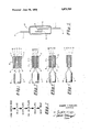
- FIG. 1 is an elevation view, partly in cross section, of a switch reed made in accordance with the teachings of this invention
- FIG. 2 is a flow diagram of a process for making the electrical Contact of the switch reed of Fig. 1;
- FIG. 3 is an elevation view, partly in cross section, of an alternate embodiment of the switch reed of Fig. 1, and
- FIG. 4 is an elevation view, partly in cross section, of another alternate embodiment of the switch reed of Fig. 1;
- FIG. 5 is an elevation view, partly in cross-section, of a reed switch assembly made in accordance with the teachings of this invention
- FIG. 6 is an elevation view, partly in cross-section, of another alternate embodiment of the switch reed of Fig. 1.
- the reed 10 comprises a cylindrical member 12 and a flat end portion 14.
- the flattened portion 14 is integral with the member 12 and the reed 10 is made from wire stock by such suitable means as a punch press or a multislide.
- the end portion 14 is preferably formed by cold working and provides a stiff structure for subsequent processing operations. The stiff structure reduces the rejection of reeds 10 due to malformed or damaged end portions 14.
- the reed 10 preferably comprises a magnetic material such, for example, as a nickel-iron alloy.
- a nickel-iron alloy such as a nickel-iron alloy.
- Suitable nickel-iron alloys comprise 51 percent by weight of nickel and the remainder iron, and 52 percent by weight nickel and the remainder iron.
- An electrical Contact 16 comprising a plurality of layers of electrically conductive material is disposed on at least a part of one surface of the end portion 14.
- the reed 10 is degreased, cleaned, and plated to form the Contact 16 with a first layer 18 of gold.
- the thickness of the layer 18 is from 0.000020 inch to 0.000060 inch. A thickness of approximately 0.000045 inch is preferred for the gold layer 18.
- the layer 18 of gold provides a basis for an efiicient electrical contact to the reed 10.
- a layer 20 of silver is disposed on the layer 18 of gold.
- the layer 20 is from 0.000005 inch to 0.000020 inch in thickness.
- a preferred thickness of the layer 20 is approximately 0.000010 inch.
- the layer 20 of silver enables silver to diffuse into the layer 18 of gold to provide a hardened wear resistant electrical Contact.
- the reed l0 and the plated layers 18 and 20 are rinsed in clear running water and a layer 22 of palladium is disposed on the layer 20 of silver.
- the thickness of the layer 22 is from 0.000015 inch to 0.000120 inch. A preferred thickness is approximately 0.000005 inch.
- the layer of palladium appears to prevent iron of the material comprising the reed 10 from diffusing through the plurality of layers to the top surface 24 of the Contact 16. This prevents the top surface 24 from being degraded electrically because of contamination by less electrically conductive material contained therein.
- the plated reed 10 is again rinsed in clear running water and a second layer 26 of gold is disposed on the layer 22 of palladium.
- the thickness of the layer 26 is from 0.000005 inch to 0.000030 inch. A preferred thickness is approximately 0.000010 inch.
- the layer 26 of gold provides an excellent electrically conductive Contact surface which is quite resistant to oxidation.
- the processed reed 10 is rinsed in clear running water, and preferably, rinsed a second time in deionized water, dried and then heat treated.
- the processed reed 10 is heated to a temperature of from l,450 to 1,650 F. for a sufficient time to diffuse the metals of the plurality of layers of the Contact 16 into one another as well as to stress relieve the end portion 14.
- a sufiicient time is provided during heat treatment to provide a preheat cycle to bake the plated areas. Baking of the plated areas enables any entrapped gases within the plated layers to be spilled without causing flaking of the plated metals or separation of the plated layers from each other or the member.
- a preferred heat treat temperature is l,650 1 15 F. for a time at temperature of from 15 to 20 minutes.
- Heat treating is preferably accomplished in an inert or a reducing atmosphere such, for example, as in hydrogen, nitrogen, argon and helium.
- the resultant Contact 16 forms an excellent electrically conductive Contact.
- the surface 24 exhibits excellent wear resistance. Any metal transfer which occurs between the op posed surfaces 24 of two switch reeds 10 employed in a switch reed assembly is of a dome-like configuration. Repeated life cycle tests of reeds 10 made in accordance with the teachings of this invention exceed the minimum of 2,000,000 cycles of a life test without the opposed contacts 16 seizing and locking together.
- a switch reed 110 which is an alternate embodiment of the reed 10.
- An item denoted by the same reference numeral in Fig. 2, as in Fig. 1, is the same item in every respect as in Fig. 1.
- the reed 110 comprises an electrical contact 112 comprising a plurality of electrical contact metals.
- the contact 112, before heat treatment, comprises the layers 18, 20 and 22 of gold, silver and palladium, respectively.
- the contact 112 is an excellent electrical contact and performs as well as the contact 16 of reed 10.
- the contact 112 has a top surface 114 which provides an excellent wear resistant surface for the contact 112.
- a switch reed 210 which is another embodiment of the switch reed 10.
- the items denoted by the reference numerals as shown in Fig. 4 are exactly the same, and function in the same manner, as the items having the same reference numerals in the Fig. 1.
- the reed 210 comprises a contact 212 disposed on at least a part of one surface of the end portion 14.
- the contact 212 comprises the plurality of layers of the same electrical contact materials as the contact 16 of reed 10, except no layer of silver is present. After the same heat treatment as the reed 10, the reed 210 functions electrically and mechanically as well as the reed 10.
- the contact 212 has a top surface 214 which shows excellent wear resistance.
- a switch reed 310 which is another embodiment of the switch reed 10.
- the items denoted by the reference numerals as shown in Fig. 6 are exactly the same, and function in the same manner, as the items having the same reference numerals in Fig. 1.
- the switch reed 310 comprises a contact disposed on at least a part of one surface of the end portion 14.
- the contact comprises only the layer 18 of gold disposed on the portion of the surface of the end portion 14 and a layer 22 of palladium disposed on the layer of gold.
- the switch reed 310 functions as well electrically and mechanically as the switch reed 10.
- a reed switch assembly 310 comprising two switch reeds 10. That portion of each of the reeds 10 which comprises the contact 16 is sealed within an envelope 312 containing a substantially inert atmosphere. Suitable materials for comprising the atmosphere of the envelope 312 are hydrogen, nitrogen, argon and a forming gas such, for example, as one comprising 97 percent by volume nitrogen and 3 percent by volume hydrogen. A portion of the member 12 of each reed l protrudes outside the envelope 312 and enables an electrical connection to be made thereto for each reed 10. A magnetic flux field is created about one or both switch reeds and the contacts 16 are attracted to each other.
- the assembly 310 is suitable for use in telephone switching equipment and the like.
- a switch reed as shown in Fig. 1, was made in accordance with the teachings of this invention and was tested, evaluated, and the results compared with those of prior art switch reeds in the following manner:
- Switch reeds comprising a magnetic material comprising 52 percent nickel and the remainder iron were manufactured on a multislide machine.
- the configuration before plating of an electrical contact on the flat end portion was as shown in Figs. 1 through 3.
- the flat end portion after forming was quite stifi' and inflexible.
- the reeds were ultrasonically degreased in Freon TF and rinsed in clear Freon TF.
- the last three-sixteenths of an inch of the flattened portion of each reed was then cleaned by soaking in an aqueons solution Metex E-l736 and rinsed in water.
- the cleaned end portions were then cleaned anodicaly for one minute at 5 volts do.
- Each reed was plated with gold to a distance of three-sixteenths of an inch from the end of the flat end portion.
- the agitated gold solution contained from 0.9 to 2.0 troy ounces of gold per gallon and had a PH of approximately 5.75, a temperature of from 120 to 140 F. and a specific gravity of about 15 Baume.
- Plating time was 8-% minutes at 700 milliamperes. The reeds were then rinsed in clear running water.
- the reeds were then plated with silver to a distance of oneeighth of an inch from the end of the flat end portion of each reed.
- the silver solution contained 3.5 troy ounces of silver per gallon and had a PH of approximately 12.5.
- the plating time was 15 seconds at 3,000 milliamperes.
- the plated reeds were rinsed in clear running water.
- the reeds were then plated with palladium to a distance of one-eighth of an inch from the end of the flattened portion of each reed.
- the palladium solution contained 5 grams of palladium per liter and had a temperature of F. and a PH of approximately 8.5.
- the plating time was 15 minutes at 900 milliamperes.
- the plated reeds were then rinsed in clean running water.
- the reeds were again gold plated. However, the plating distance was only one-eighth of an inch from the end of the flattened portion and the plating time was only approximately 3 minutes.
- the plated reeds were rinsed in clean running water initially. The reeds were rinsed a second time in deionized water and dried at approximately 320 i 10 F. in a circulating air furnace.
- the plated reeds were examined visually.
- the plated end portions had a yellow appearance of gold.
- Several reeds were sectioned, mounted and examined. The plated areas were clearly visible.
- the first gold layer had an average thickness of about 0.000045 of an inch.
- the average thickness of the silver layer was about 0.000010 of an inch.
- the average thickness of the palladium layer was about 0.000005.
- the second gold layer had an average thickness of about 0.000015 of an inch.
- the remaining plated reeds were heated to a temperature of about 1,650 1 15 F. for from 15 to 20 minutes at temperature. Heat treating was done in an atmosphere of hydrogen having a dew point of 50 C. and a flow rate of 15 cubic feet per hour. The reeds were cooled to room temperature in flowing hydrogen gas.
- the remaining reeds were then mounted in a life test fixtured and cycled at cycles per second to evaluate the plated contact of the flat end portion.
- the test duplicated normal contact operation of making and breaking at 50 volts and 0.070 ampere. A completion of a minimum of 2,000,000 cycles is required to be acceptable for telephony equipment.
- a second group of prior art reeds, each having an electrical contact comprising layers of palladium, gold, silver and gold metals disposed one upon the other were life cycled in the same manner as the plated reeds of this invention.
- the prior art reeds failed by seizing before 2,000,000 cycles had been completed.
- a peak cone transfer of metal between two opposed contacts caused a direct short circuit between the opposed contacts.
- Switch reeds made in accordance with this invention are therefore excellent reed components for reed switch assemblies.
- some prior art assemblies required opposed electrical contacts to be of dissimilar metals
- a reed switch assembly of this invention utilizes the same electrical contact metal structure for the switch reeds. This eliminates the requirement of two different components and optimizes production capabilities and results in a superior reed switch assembly of greater reliability.
- a switch reed comprising:
- a body of electrically conductive magnetic material having at least an integral flat end portion
- an electrical contact disposed on, and in an electrical conductive relationship with at least a part of one of the surfaces of the flat end portion and initially comprising before heat treatment, a plurality of layers of electrically conductive metals disposed one upon the other including;
- said layer of gold has an initial thickness of from 0.000020 to 0.000060 inch said layer of silver has an initial thickness of from 0.00005 to 0.000020 inch, and
- said layer of palladium has an initial thickness of from 4.
- the layer of gold has an initial thickness of approximately 0.000045 inch
- the layer of silver has an initial thickness of approximately 0.000010 inch
- the layer of palladium as an initial thickness of approximately 0.00005 inch.
- a layer of gold of from 0.00005 inch to 0.000030 inch in thickness initially disposed on said layer of palladium.
- the layer of gold on said layer of palladium is approximately 0.000015 inch in thickness initially.
- a reed switch assembly comprising:
- each switch reed comprising a body of electrically conductive magnetic material having-at least an integral flattened end portion, an electrical contact disposed on, and in an electrical conductive relationship with at least a part of one of the surfaces of the flattened portion and initially comprising, before heat treatment, a plurality of electrically conductive metal layers disposed one upon the other and comprising at least a layer of gold disposed on at least one surface of a part of the flattened end portion and a layer of palladium, the flattened portion of each switch reed being incorporated within said envelope and spaced apart from the other flattened portion, the contacts of said reeds being disposed spaced apart and opposed to one another.
- said layers of gold has an initial thickness of from 0.000020 to 0.000060 inch;
- said layer of silver has an initial thickness of from 0.000005 to 0.000020 inch
- said layer of palladium has an initial thickness of from 0.000015 to 0.000120 inch.
- said contact comprises a second layer of gold disposed on, and is an electrically conductive relationship with, said layer of palladium, said layer of gold having an initial thickness of from 0.000005 inch to 0.000030 inch.
- said layer of gold initially has a thickness of approximately 0.000045 inch
- said layer of silver initially has a thickness of approximately 0.000010 inch
- said layer of palladium has an initial thickness of approximately 0.00005 inch
- said second layer of gold has an initial thickness of approximately 0.000015 inch.
- Col 2, line 3h "0.000005" should be ---0.00005-.
Landscapes
- Contacts (AREA)
Abstract
Description
Claims (10)
- 2. The switch reed of claim 1 and including: a layer of silver disposed between and in abutting electrical contact with, said layers of gold and palladium.
- 3. The switch reed of claim 2 wherein: said layer of gold has an initial thickness of from 0.000020 to 0.000060 inch; said layer of silver has an initial thickness of from 0.00005 to 0.000020 inch, and said layer of palladium has an initial thickness of from 0.000015 to 0.000120.
- 4. The switch reed of claim 2 wherein: the layer of gold has an initial thickness of approximately 0.000045 inch; the layer of silver has an initial thickness of approximately 0.000010 inch, and the layer of palladium as an initial thickness of approximately 0.00005 inch.
- 5. The switch reed of claim 2 including: a layer of gold disposed on said layer of palladium.
- 6. The switch reed of claim 3 including: a layer of gold of from 0.00005 inch to 0.000030 inch in thickness initially disposed on said layer of palladium.
- 7. The switch reed of claim 6 wherein: the layer of gold on said layer of palladium is approximately 0.000015 inch in thickness initially.
- 8. A reed switch assembly comprising: an envelope, and a pair of switch reeds, each reed comprising a body of electrically conductive magnetic material having at least an integral flattened end portion, an electrical contact disposed on, and in an electrical conductive relationship with at least a part of one of the surfaces of the flattened portion and initially comprising, before heat treatment, a plurality of electrically conductive metal layers disposed one upon the other and comprising at least a layer of gold disposed on at least one surface of a part of the flattened end portion and a layer of palladium, the flattened portion of each switch reed being incorporated within said envelope and spaced apart from the other flattened portion, the contacts of said reeds being disposed spaced apart and opposed to one another.
- 9. The reed switch assembly of claim 8 in which said contact comprises: a layer of silver disposed between and in abutting electrical contact with said layers of gold and palladium; and said layers of gold has an initial thickness of from 0.000020 to 0.000060 inch; said layer of silver has an initial thickness of from 0.000005 to 0.000020 inch, and said layer of palladium has an initial thickness of from 0.000015 to 0.000120 inch.
- 10. The reed switch assembly of claim 9 in which: said contact comprises a second layer of gold disposed on, and is an electrically conductive relationship with, said layer of palladium, said layer of gold having an initial thickness of from 0.000005 inch to 0.000030 inch.
- 11. The reed switch assembly of claim 10 in which: said layer of gold initially has a thickness of approximately 0.000045 inch; said layer of silver initially has a thickness of approximately 0.000010 inch; said layer of palladium has an initial thickness of approximately 0.00005 inch, and said second layer of gold has an initial thickness of approximately 0.000015 inch.
Applications Claiming Priority (1)
| Application Number | Priority Date | Filing Date | Title |
|---|---|---|---|
| US12431271A | 1971-03-15 | 1971-03-15 |
Publications (1)
| Publication Number | Publication Date |
|---|---|
| US3671702A true US3671702A (en) | 1972-06-20 |
Family
ID=22414113
Family Applications (1)
| Application Number | Title | Priority Date | Filing Date |
|---|---|---|---|
| US124312A Expired - Lifetime US3671702A (en) | 1971-03-15 | 1971-03-15 | An electrical contact structure for a switch reed comprising gold and palladium layers |
Country Status (1)
| Country | Link |
|---|---|
| US (1) | US3671702A (en) |
Cited By (5)
| Publication number | Priority date | Publication date | Assignee | Title |
|---|---|---|---|---|
| US4105828A (en) * | 1976-02-02 | 1978-08-08 | Siemens Aktiengesellschaft | Low-current contact construction |
| US4117291A (en) * | 1977-05-19 | 1978-09-26 | Gte Automatic Electric Laboratories Incorporated | Reed switch |
| US4138604A (en) * | 1975-09-13 | 1979-02-06 | W. C. Heraeus Gmbh | Electrical plug-type connector |
| US5438175A (en) * | 1992-12-22 | 1995-08-01 | W. C. Heraeus Gmbh | Electric outlet element having double flash |
| US20040113714A1 (en) * | 2002-12-16 | 2004-06-17 | Com Dev Ltd. | Incomplete mechanical contacts for microwave switches |
Citations (2)
| Publication number | Priority date | Publication date | Assignee | Title |
|---|---|---|---|---|
| US2897584A (en) * | 1957-05-22 | 1959-08-04 | Sel Rex Corp | Gold plated electrical contact and similar elements |
| US3214558A (en) * | 1961-08-25 | 1965-10-26 | Siemens Ag | Contact arrangement exhibiting reduced material migration |
-
1971
- 1971-03-15 US US124312A patent/US3671702A/en not_active Expired - Lifetime
Patent Citations (2)
| Publication number | Priority date | Publication date | Assignee | Title |
|---|---|---|---|---|
| US2897584A (en) * | 1957-05-22 | 1959-08-04 | Sel Rex Corp | Gold plated electrical contact and similar elements |
| US3214558A (en) * | 1961-08-25 | 1965-10-26 | Siemens Ag | Contact arrangement exhibiting reduced material migration |
Cited By (6)
| Publication number | Priority date | Publication date | Assignee | Title |
|---|---|---|---|---|
| US4138604A (en) * | 1975-09-13 | 1979-02-06 | W. C. Heraeus Gmbh | Electrical plug-type connector |
| US4105828A (en) * | 1976-02-02 | 1978-08-08 | Siemens Aktiengesellschaft | Low-current contact construction |
| US4117291A (en) * | 1977-05-19 | 1978-09-26 | Gte Automatic Electric Laboratories Incorporated | Reed switch |
| US5438175A (en) * | 1992-12-22 | 1995-08-01 | W. C. Heraeus Gmbh | Electric outlet element having double flash |
| US20040113714A1 (en) * | 2002-12-16 | 2004-06-17 | Com Dev Ltd. | Incomplete mechanical contacts for microwave switches |
| US6856212B2 (en) | 2002-12-16 | 2005-02-15 | Com Dev Ltd. | Incomplete mechanical contacts for microwave switches |
Similar Documents
| Publication | Publication Date | Title |
|---|---|---|
| US7923651B2 (en) | Silver-coated stainless steel strip for movable contacts and method of producing the same | |
| US3671702A (en) | An electrical contact structure for a switch reed comprising gold and palladium layers | |
| US20040038072A1 (en) | Terminal with ruthenium layer and part having the same | |
| US2391458A (en) | Spark gap electrode | |
| US20120301745A1 (en) | Silver-coated composite material for a movable contact part, method of producing the same, and movable contact part | |
| US3249728A (en) | Reed switch having multi-layer diffused contacts | |
| US3443312A (en) | Method of making gas-filled enclosed switchgear with copper contacts | |
| US2600175A (en) | Electrical contact | |
| US3641300A (en) | Electrical contact | |
| US3697389A (en) | Method of forming electrical contact materials | |
| US3889366A (en) | Method for producing electric contacts made of internally oxidized silver alloy | |
| ES461997A1 (en) | PROCEDURE FOR THE MANUFACTURE OF ONE SILVER CONTACT PIECE AND AT LEAST TWO UNNEWABLE METAL OXIDES. | |
| Schoepf et al. | Effects of different loads on the surface of silver metal oxide contacts for general-purpose relays | |
| US3497655A (en) | Clad metal contacts for reed switches | |
| US3495061A (en) | Contacts for reed switches | |
| US3668355A (en) | Reed material for sealed contact application | |
| GB1104485A (en) | Switching devices | |
| US3644692A (en) | Osmium plated contacts | |
| US3146328A (en) | Non-sticking electrical contacts | |
| US3267302A (en) | Apparatus and method of contact conditioning | |
| KR102417333B1 (en) | An electrical contact materials | |
| RU2215342C2 (en) | Surface coating of high-power ferreed contacts (alternatives) | |
| US4348566A (en) | Rhodium electrical contact of a switch particularly a reed switch | |
| US3319200A (en) | Electrical relay having coaxial terminals | |
| Beattie | Palladium plating on telephone plugs and sockets |
Legal Events
| Date | Code | Title | Description |
|---|---|---|---|
| AS | Assignment |
Owner name: GENERAL DYNAMICS TELEQUIPMENT CORPORATION Free format text: CHANGE OF NAME;ASSIGNOR:STROMBERG-CARLSON CORPORATION;REEL/FRAME:004157/0746 Effective date: 19821221 Owner name: GENERAL DYNAMICS TELEPHONE SYSTEMS CENTER INC., Free format text: CHANGE OF NAME;ASSIGNOR:GENERAL DYNAMICS TELEQUIPMENT CORPORATION;REEL/FRAME:004157/0723 Effective date: 19830124 Owner name: UNITED TECHNOLOGIES CORPORATION, A DE CORP. Free format text: ASSIGNMENT OF ASSIGNORS INTEREST.;ASSIGNOR:GENERAL DYNAMICS TELEPHONE SYSTEMS CENTER INC.;REEL/FRAME:004157/0698 Effective date: 19830519 |
|
| AS | Assignment |
Owner name: GEC PLESSEY TELECOMMUNICATIONS LIMITED, ENGLAND Free format text: ASSIGNMENT OF ASSIGNORS INTEREST.;ASSIGNORS:STROMBERG-CARLSON CORPORATION, A DE CORPORATION;PLESSEY-UK LIMITED;REEL/FRAME:005733/0547;SIGNING DATES FROM 19820917 TO 19890918 Owner name: STROMBERG-CARLSON CORPORATION, FLORIDA Free format text: ASSIGNMENT OF ASSIGNORS INTEREST.;ASSIGNOR:UNITED TECHNOLOGIES CORPORATION A CORPORATION OF DE;REEL/FRAME:005732/0982 Effective date: 19850605 |