US3546589A - Frequency characteristic shaping circuits - Google Patents
Frequency characteristic shaping circuits Download PDFInfo
- Publication number
- US3546589A US3546589A US645093A US3546589DA US3546589A US 3546589 A US3546589 A US 3546589A US 645093 A US645093 A US 645093A US 3546589D A US3546589D A US 3546589DA US 3546589 A US3546589 A US 3546589A
- Authority
- US
- United States
- Prior art keywords
- input
- output
- frequency
- modulator
- unit
- Prior art date
- Legal status (The legal status is an assumption and is not a legal conclusion. Google has not performed a legal analysis and makes no representation as to the accuracy of the status listed.)
- Expired - Lifetime
Links
- 238000007493 shaping process Methods 0.000 title description 4
- 238000013519 translation Methods 0.000 description 17
- 230000014616 translation Effects 0.000 description 17
- 238000001228 spectrum Methods 0.000 description 13
- 230000010363 phase shift Effects 0.000 description 12
- 238000010586 diagram Methods 0.000 description 8
- 238000005070 sampling Methods 0.000 description 5
- 230000001629 suppression Effects 0.000 description 5
- 230000003111 delayed effect Effects 0.000 description 2
- 238000000034 method Methods 0.000 description 2
- 230000002441 reversible effect Effects 0.000 description 2
- 230000008878 coupling Effects 0.000 description 1
- 238000010168 coupling process Methods 0.000 description 1
- 238000005859 coupling reaction Methods 0.000 description 1
- 230000010354 integration Effects 0.000 description 1
- 230000010355 oscillation Effects 0.000 description 1
- 230000001131 transforming effect Effects 0.000 description 1
Images


Classifications
-
- H—ELECTRICITY
- H03—ELECTRONIC CIRCUITRY
- H03D—DEMODULATION OR TRANSFERENCE OF MODULATION FROM ONE CARRIER TO ANOTHER
- H03D7/00—Transference of modulation from one carrier to another, e.g. frequency-changing
-
- H—ELECTRICITY
- H04—ELECTRIC COMMUNICATION TECHNIQUE
- H04J—MULTIPLEX COMMUNICATION
- H04J1/00—Frequency-division multiplex systems
- H04J1/02—Details
- H04J1/04—Frequency-transposition arrangements
-
- H—ELECTRICITY
- H03—ELECTRONIC CIRCUITRY
- H03B—GENERATION OF OSCILLATIONS, DIRECTLY OR BY FREQUENCY-CHANGING, BY CIRCUITS EMPLOYING ACTIVE ELEMENTS WHICH OPERATE IN A NON-SWITCHING MANNER; GENERATION OF NOISE BY SUCH CIRCUITS
- H03B21/00—Generation of oscillations by combining unmodulated signals of different frequencies
-
- H—ELECTRICITY
- H03—ELECTRONIC CIRCUITRY
- H03B—GENERATION OF OSCILLATIONS, DIRECTLY OR BY FREQUENCY-CHANGING, BY CIRCUITS EMPLOYING ACTIVE ELEMENTS WHICH OPERATE IN A NON-SWITCHING MANNER; GENERATION OF NOISE BY SUCH CIRCUITS
- H03B27/00—Generation of oscillations providing a plurality of outputs of the same frequency but differing in phase, other than merely two anti-phase outputs
-
- H—ELECTRICITY
- H03—ELECTRONIC CIRCUITRY
- H03C—MODULATION
- H03C1/00—Amplitude modulation
- H03C1/52—Modulators in which carrier or one sideband is wholly or partially suppressed
- H03C1/60—Modulators in which carrier or one sideband is wholly or partially suppressed with one sideband wholly or partially suppressed
-
- H—ELECTRICITY
- H03—ELECTRONIC CIRCUITRY
- H03D—DEMODULATION OR TRANSFERENCE OF MODULATION FROM ONE CARRIER TO ANOTHER
- H03D2200/00—Indexing scheme relating to details of demodulation or transference of modulation from one carrier to another covered by H03D
- H03D2200/0041—Functional aspects of demodulators
- H03D2200/006—Signal sampling
-
- H—ELECTRICITY
- H03—ELECTRONIC CIRCUITRY
- H03D—DEMODULATION OR TRANSFERENCE OF MODULATION FROM ONE CARRIER TO ANOTHER
- H03D2200/00—Indexing scheme relating to details of demodulation or transference of modulation from one carrier to another covered by H03D
- H03D2200/0041—Functional aspects of demodulators
- H03D2200/0066—Mixing
- H03D2200/0078—Mixing using a switched phase shifter or delay line
-
- H—ELECTRICITY
- H03—ELECTRONIC CIRCUITRY
- H03D—DEMODULATION OR TRANSFERENCE OF MODULATION FROM ONE CARRIER TO ANOTHER
- H03D7/00—Transference of modulation from one carrier to another, e.g. frequency-changing
- H03D7/16—Multiple-frequency-changing
- H03D7/161—Multiple-frequency-changing all the frequency changers being connected in cascade
- H03D7/163—Multiple-frequency-changing all the frequency changers being connected in cascade the local oscillations of at least two of the frequency changers being derived from a single oscillator
-
- H—ELECTRICITY
- H03—ELECTRONIC CIRCUITRY
- H03D—DEMODULATION OR TRANSFERENCE OF MODULATION FROM ONE CARRIER TO ANOTHER
- H03D7/00—Transference of modulation from one carrier to another, e.g. frequency-changing
- H03D7/16—Multiple-frequency-changing
- H03D7/165—Multiple-frequency-changing at least two frequency changers being located in different paths, e.g. in two paths with carriers in quadrature
Definitions
- the output from the N output paths are summed to provide output frequency spectrums which are either an erect or inverted translation of the input frequency spectrumr
- the invention relates to N-path frequency translation systems or frequency characteristic shaping circuits. Such systems are useful for providing frequency functions (certain bandpass characteristics) otherwise commonly pro- 4 vided by modulators and complicated filters.
- the ⁇ invention provides an 'N-path frequency translation system comprising an input polyphase modulator unit having N-output paths which are identical and connected in parallel," each of said output'pat'hs which comprises a filter unit and at least one output modulator unit sample in turn a given input frequency spectrum for a period of time determined by; N, said input polyphase modulator unit and said output modulator units being unbalanced, the outputs of each of said output paths being connected to a summation unit the output frequency l spectrums of which are either an erect or inverted tr'anslat'ionof said input fre'qu'ency spectrum.
- an N-path frequencyitranslation system as detailed in the preceding paragraph is provided wherein said input frequency spectrum is hand limited by providing a second filter unit which is interposed between said input and said input polyphase modulator unit.
- an N-path frequency translation system as detailed in the preceding paragraphs is provided wherein said input polyphase modulator 'unitc'omprises an N-pole, N-way rotary sampling switch andN-phase' shift networks, each of said phase shift networks being connected between the input terminal and the wiper arm of one of said-N-poles,
- each of said wiper arms lags behind the preceding one by an amount 21n/N degrees, and'w-herein each of According to another feature of the invention an N path frequency translation system as detailed in the preceding paragraphs is provided wherein said output modulator said phase shift networks lagsvbehind the preceding one .units are provided by a polyphase demodulator unit.
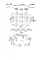
- FIG. 1 shows a block diagram of the N-p'ath configuration of a frequency translation system
- FIG. 2 shows a block diagram of the n -path of the frequency translation system shown in the drawing according to FIG. 1;
- FIG. 3 shows a block diagram of a practical circuit for realisation of the N-path configuration of the frequency translation system shown in the drawing according to FIG. 1;
- FIG. 4 shows a waveform which expresses the function of the modulator shown in the drawing according to FIG. 3;
- FIG. 5 shows part of the output spectrum of a frequency translation system
- FIG. 6 shows a block diagram of a practical circuit for part of a three-Way frequency translation 1 system for realisation of supplementary polyphase modulation
- FIG. 7 shows a block diagram of a part of a practical circuit for the general case for realisation of supplementary polyphase modulation.
- FIG. 1 a block diagram of the N-path configuration of a frequency translation system is shown
- each path of which comprises a modulator unit 1 at a frequency f which is the midband frequency of the input band of frequencies, a low pass filter unit 2 whose cut-off frequency is half the desired system bandwidth and'a second modulator unit 3 at a frequency f which is the midband frequency of the output band frequencies.
- the modulator units 1 and 3 being unbalanced.
- This system is arranged to select a band of frequencies from a given input spectrum and to translate it either erect or inverted to a new frequency band, i.e. the output frequency band as obtained from the summation unit 4.
- the output signal is sampled by and passed through the input modulator unit 1.
- This modulator unit has a square wave signal applied to it so there will be a large number of frequency components appearing in the output circuit of the input modulator unit 1 but the only one of interest is the difference frequency between the input and modulator frequencies.
- the output from the low pass filter unit 2 will be a single low frequency signal which is demodulated by the output modulator unit 3 before being passed to the summation unit 4.
- each of the units may be expressed as a function of time (t) in terms of the input and output voltages as follows:
- r( t) is the transfer function of the modulator unit 1
- h(t) is the transfer function of the low pass filter unit 2
- q(t) is the transfer function of the modulator unit 3.
- the modulating or switching functions are defined by the Fourier Series sion of input modulator switching functions.
- FIG. 3 a block diagram of a practical circuit for realization of the N-path configuration of a frequency translation system is shown, the two modulators in each path being replaced by rotary sampling switches SW1 and SW2.
- the input modulator has a shorting ring 5 which rotates in synchronism with the switch and earths the inputs to all the low pass filter units 2 except the one which makes contact with the input switch SW1.
- the modulator function can be expressed as'shown in FIG. 4.
- the low pass filter requirements are considerably reduced and a suppression of the unwanted signal of approximately to 40 db is obtained.
- FIG. 6 is a block diagram of a practical circuit for part of a 3-way frequency translation system for realisation of supplementary polyphase modulation is shown, the unbalanced input modulators 1 shown in the drawing according to FIG. 1 being replaced by a 3-pole, 3-way rotary sampling switch SW3.
- phase shift networks Interposed between the input terminal and each of the 3 poles of the switch SW3 are phase shift networks which are connected to the wiper arms of the three poles of the switch SW3.
- Each wiper arm lags behind the preceding one by an amount 21r/N degrees and each phase shift network lags behind the preceding one by an amount 21r/N degrees. Therefore in the 3-path system the wiper arm and the associated phase shift network lag behind the preceding ones by
- the low pass filter units 2 in each of the three paths are connected to their respective output terminals 1, 2, and 3 on all of the three poles of the switch SW3.
- a frequency characteristic shaping system using time varying means for transforming input frequency spectrums to output frequency spectrums
- said system comprising a first input polyphase modulator unit
- said input polyphase modulator unit comprising a first rotary switch having a plurality of poles
- said second modulator unit comprising a second rotary switch having a plurality of poles
- the wiper of said first switch rotating at a first angular velocity and maintaining contact with each pole for a period equal to the time period of said first angular velocity divided by the number of poles
- the wiper of the second switch rotating at a second angular velocity and maintaining contact with each pole for a period equal to the time period of said second angular velocity divided by the number of poles
- said output wiper connected to a summation unit whereby said input frequency characteristics is modulated, filtered, re-modulated and summed to provide a translated frequency characteristic at the output of said summation unit.
- each of said paths coupled to the wipers of said first switch comprises a phase shift network and wherein the output of each of said phase shift networks lags the preceding one of said phase shift networks by 21r/N degrees, where N is the number of poles.
- said second modulator unit comprises an N-pole, N-way rotary sampling switch and N phase shift networks
- each of said phase shift networks being connected between said summation unit and wiper arm of one of said N-poles, wherein each of said wiper arms lags behind preceding one by an amount of 21r/N degrees, and wherein each of said summation networks lags behind the preceding one by an amount 21r/N degrees.
Landscapes
- Engineering & Computer Science (AREA)
- Physics & Mathematics (AREA)
- Electromagnetism (AREA)
- Computer Networks & Wireless Communication (AREA)
- Signal Processing (AREA)
- Power Engineering (AREA)
- Amplitude Modulation (AREA)
- Facsimile Scanning Arrangements (AREA)
- Digital Transmission Methods That Use Modulated Carrier Waves (AREA)
Applications Claiming Priority (1)
| Application Number | Priority Date | Filing Date | Title |
|---|---|---|---|
| GB24792/66A GB1112248A (en) | 1966-06-03 | 1966-06-03 | Improvements in or relating to n-path frequency translation systems |
Publications (1)
| Publication Number | Publication Date |
|---|---|
| US3546589A true US3546589A (en) | 1970-12-08 |
Family
ID=10217308
Family Applications (1)
| Application Number | Title | Priority Date | Filing Date |
|---|---|---|---|
| US645093A Expired - Lifetime US3546589A (en) | 1966-06-03 | 1967-06-01 | Frequency characteristic shaping circuits |
Country Status (7)
| Country | Link |
|---|---|
| US (1) | US3546589A (enExample) |
| BE (1) | BE699455A (enExample) |
| CH (1) | CH507618A (enExample) |
| DE (1) | DE1591197A1 (enExample) |
| GB (1) | GB1112248A (enExample) |
| NL (1) | NL6707818A (enExample) |
| SE (1) | SE335558B (enExample) |
Cited By (1)
| Publication number | Priority date | Publication date | Assignee | Title |
|---|---|---|---|---|
| US4004238A (en) * | 1974-12-14 | 1977-01-18 | Eltro Gmbh Gesellschaft Fur Strahlungstechnik | Method and apparatus for the removal of ringing phenomena from signal impulses |
Citations (8)
| Publication number | Priority date | Publication date | Assignee | Title |
|---|---|---|---|---|
| US1850569A (en) * | 1927-06-25 | 1932-03-22 | Telefunken Gmbh | Radio receiving system |
| US2526425A (en) * | 1947-10-28 | 1950-10-17 | Bendix Aviat Corp | Radio-telemetering with phase modulation |
| US2527649A (en) * | 1949-02-18 | 1950-10-31 | Bell Telephone Labor Inc | Synchronization of pulse transmission systems |
| DE1023801B (de) * | 1956-07-19 | 1958-02-06 | Siemens Ag | Nachrichtenuebertragungssystem nach Art eines Traegerfrequenzsystems |
| US2852606A (en) * | 1952-09-17 | 1958-09-16 | Curry Paul | Electrical communication systems and method of transmitting energy |
| US3081434A (en) * | 1960-04-18 | 1963-03-12 | Bell Telephone Labor Inc | Multibranch circuits for translating frequency characteristics |
| US3205310A (en) * | 1960-03-08 | 1965-09-07 | Siemens Ag | Low loss arrangement for conversion of frequency bands, utilizing a switching circuit |
| US3406383A (en) * | 1964-08-21 | 1968-10-15 | Robertshaw Controls Co | Analog keyed phase transmitter and system |
-
1966
- 1966-06-03 GB GB24792/66A patent/GB1112248A/en not_active Expired
-
1967
- 1967-06-01 US US645093A patent/US3546589A/en not_active Expired - Lifetime
- 1967-06-01 DE DE19671591197 patent/DE1591197A1/de active Pending
- 1967-06-02 CH CH787167A patent/CH507618A/de not_active IP Right Cessation
- 1967-06-05 BE BE699455D patent/BE699455A/xx unknown
- 1967-06-05 NL NL6707818A patent/NL6707818A/xx unknown
- 1967-06-05 SE SE07827/67A patent/SE335558B/xx unknown
Patent Citations (8)
| Publication number | Priority date | Publication date | Assignee | Title |
|---|---|---|---|---|
| US1850569A (en) * | 1927-06-25 | 1932-03-22 | Telefunken Gmbh | Radio receiving system |
| US2526425A (en) * | 1947-10-28 | 1950-10-17 | Bendix Aviat Corp | Radio-telemetering with phase modulation |
| US2527649A (en) * | 1949-02-18 | 1950-10-31 | Bell Telephone Labor Inc | Synchronization of pulse transmission systems |
| US2852606A (en) * | 1952-09-17 | 1958-09-16 | Curry Paul | Electrical communication systems and method of transmitting energy |
| DE1023801B (de) * | 1956-07-19 | 1958-02-06 | Siemens Ag | Nachrichtenuebertragungssystem nach Art eines Traegerfrequenzsystems |
| US3205310A (en) * | 1960-03-08 | 1965-09-07 | Siemens Ag | Low loss arrangement for conversion of frequency bands, utilizing a switching circuit |
| US3081434A (en) * | 1960-04-18 | 1963-03-12 | Bell Telephone Labor Inc | Multibranch circuits for translating frequency characteristics |
| US3406383A (en) * | 1964-08-21 | 1968-10-15 | Robertshaw Controls Co | Analog keyed phase transmitter and system |
Cited By (1)
| Publication number | Priority date | Publication date | Assignee | Title |
|---|---|---|---|---|
| US4004238A (en) * | 1974-12-14 | 1977-01-18 | Eltro Gmbh Gesellschaft Fur Strahlungstechnik | Method and apparatus for the removal of ringing phenomena from signal impulses |
Also Published As
| Publication number | Publication date |
|---|---|
| BE699455A (enExample) | 1967-12-05 |
| NL6707818A (enExample) | 1967-12-04 |
| CH507618A (de) | 1971-05-15 |
| GB1112248A (en) | 1968-05-01 |
| DE1591197A1 (de) | 1971-02-18 |
| SE335558B (enExample) | 1971-06-01 |
Similar Documents
| Publication | Publication Date | Title |
|---|---|---|
| Ziemer et al. | Conversion and matched filter approximations for serial minimum-shift keyed modulation | |
| US3649922A (en) | Digital waveform generator | |
| US4123712A (en) | Symmetrical polyphase network | |
| US3559042A (en) | Polyphase symmetrical network | |
| US3493876A (en) | Stable coherent filter for sampled bandpass signals | |
| US3971922A (en) | Circuit arrangement for digitally processing a given number of channel signals | |
| US3500217A (en) | Frequency discriminator employing quadrature demodulation techniques | |
| US3546589A (en) | Frequency characteristic shaping circuits | |
| US2797314A (en) | Demodulation of vestigial sideband signals | |
| US3562556A (en) | N-path frequency translation system | |
| US2758204A (en) | Wide-band phase shifter network | |
| US4455539A (en) | Switched capacitor all pass filter | |
| US3585529A (en) | Single-sideband modulator | |
| Sun et al. | A general theory of commutated networks | |
| US3628163A (en) | Filter system | |
| US3585503A (en) | Binary psk transmission using two closely related frequencies to eliminate phase discontinuity | |
| US2897456A (en) | Dissipationless differential phase shifters | |
| US3896437A (en) | Apparatus for generating precise crossover frequency of two independent equal bandwidth spectra | |
| Saraga | New class of time-varying filters | |
| RU2012150C1 (ru) | Частотный модулятор | |
| GB517516A (en) | Improvements in or relating to electric wave transmission networks | |
| Dillon | Sensitivity considerations in cascaded lattice-type quadrature-modulation networks | |
| SU1107267A1 (ru) | Балансный фазовый детектор с квадратурным выходом | |
| Patangia et al. | A digitally controlled tunable N-path filter | |
| Gawargy et al. | Economic implementation of a high performance FDM system using the sequence discriminator |
Legal Events
| Date | Code | Title | Description |
|---|---|---|---|
| AS | Assignment |
Owner name: STC PLC,ENGLAND Free format text: ASSIGNMENT OF ASSIGNORS INTEREST;ASSIGNOR:INTERNATIONAL STANDARD ELECTRIC CORPORATION, A DE CORP.;REEL/FRAME:004761/0721 Effective date: 19870423 Owner name: STC PLC, 10 MALTRAVERS STREET, LONDON, WC2R 3HA, E Free format text: ASSIGNMENT OF ASSIGNORS INTEREST.;ASSIGNOR:INTERNATIONAL STANDARD ELECTRIC CORPORATION, A DE CORP.;REEL/FRAME:004761/0721 Effective date: 19870423 |