US3290536A - Electroluminescent lamp with homogeneous phosphor-dielectric layer - Google Patents
Electroluminescent lamp with homogeneous phosphor-dielectric layer Download PDFInfo
- Publication number
- US3290536A US3290536A US163758A US16375862A US3290536A US 3290536 A US3290536 A US 3290536A US 163758 A US163758 A US 163758A US 16375862 A US16375862 A US 16375862A US 3290536 A US3290536 A US 3290536A
- Authority
- US
- United States
- Prior art keywords
- layer
- phosphor
- dielectric
- conductive
- dielectric layer
- Prior art date
- Legal status (The legal status is an assumption and is not a legal conclusion. Google has not performed a legal analysis and makes no representation as to the accuracy of the status listed.)
- Expired - Lifetime
Links
Images
Classifications
-
- H—ELECTRICITY
- H05—ELECTRIC TECHNIQUES NOT OTHERWISE PROVIDED FOR
- H05B—ELECTRIC HEATING; ELECTRIC LIGHT SOURCES NOT OTHERWISE PROVIDED FOR; CIRCUIT ARRANGEMENTS FOR ELECTRIC LIGHT SOURCES, IN GENERAL
- H05B33/00—Electroluminescent light sources
- H05B33/12—Light sources with substantially two-dimensional [2D] radiating surfaces
- H05B33/22—Light sources with substantially two-dimensional [2D] radiating surfaces characterised by the chemical or physical composition or the arrangement of auxiliary dielectric or reflective layers
-
- H—ELECTRICITY
- H05—ELECTRIC TECHNIQUES NOT OTHERWISE PROVIDED FOR
- H05B—ELECTRIC HEATING; ELECTRIC LIGHT SOURCES NOT OTHERWISE PROVIDED FOR; CIRCUIT ARRANGEMENTS FOR ELECTRIC LIGHT SOURCES, IN GENERAL
- H05B33/00—Electroluminescent light sources
- H05B33/12—Light sources with substantially two-dimensional [2D] radiating surfaces
- H05B33/20—Light sources with substantially two-dimensional [2D] radiating surfaces characterised by the chemical or physical composition or the arrangement of the material in which the electroluminescent material is embedded
Definitions
- the invention relates to electroluminescent lamps and to the manufacture thereof.
- Such lamps have :a light-transmitting piece of material with a light-transmitting, electrically-conducting surface, a mixture of phosphor and dielectric substance coated thereover, and a conductive backing layer over the phosphor. Light is emitted from the device when a voltage is applied between the conductive backing layer and the conducting surface of the material.
- the dielectric coating can be of lacquer, wax, plastic or other material of high resistivity, dielectric constant, and dielectric strength, and inactive chemically with the backing layer and the phosphor-dielectric layer.
- Such a coating would be expected to cause a diminution in light output from the lamp, because of the voltage drop in the coating, but I find that instead the light output is about the same as that without the coating, at least after a short aging period.
- the maintenance of light output during life can be still further increased by the use of an alloy of aluminum and cop-per as the material of the conuctive backing layer.
- the glass plate 1 in that embodiment carries on its surface the light-transmitting electrically-conductive layer or coating 2, in contact with the metal strip 3 which preferably extends over the corresponding edge of the glass plate 1, in the -L-shape shown.
- a similarL-shaped metal strip 4 is affixed to the opposite edge of the glass plate 1 as shown, it being iafiixed to a portion thereof to which the conductive-coating 2 does notextend.
- the conductive backing layer 7 is applied over the dielectric layer 6, at least in part, and extends into cont-act with the metal strip 4, although it must not also extend into contact with the metal strip 3 which-is connected electrically to the transparent conductive layer 2, as that would simply short circuit the device.
- the conducting surface or layer 2 should be durable, inactive chemically with respect to the other materials used in the lamp, and of good light-transmission.
- a durable, chemically-inactive conducting surface 2 of good light-transmission either transparency or translucency, is difiicult to obtain, because good electric conductors are generally good reflectors of light, rather than transmitters of it.
- the resultant conductive surface appears to be a layer 2 of stannic (or silicic or titanic) oxide, probably to some extent at least reduced to a form lower than the dioxide, although the exact composition is difficu'lt to determine.
- the resistance of the conductive surface 2 should be low enough to avoid excessive power loss therein at the current used.
- One side of the glass plate 1 can be completely coated with the conducting layer 2, if desired, and then the portion of layer 2 in the vicinity of the position desired for the application of the metal strip 4, which must be out of electrical contact with said conducting layer 2, can be re- 'moved by applying to that portion a mixture of zinc dust mixed with sutficient zinc dust to'form a thick slurry has been found very effective.
- the metal strips 3 and 4 are coatings painted onto the glass piece 1 (over the conducting layer 2 in the case of strip 3) by using one of the conducting silver paints of the firing type know in the art and commonly on the market. After application, the paint is fired to the glass at about 1000 F.
- Silver paints'of the 'air-dried-type can be used, but do not afford the permanent metal-to-glass bond that can be obtained with the fired paints. Spraying and other forms of metal deposition can be used instead of painting, .if
- both contact-strips 3 and 4 may be placed along different portions of a single edge of the glass plate '1, the conductive layer 2 being in contact with the first of said strips and out of contact with the other, and
- the backing layer 6 being out of contact with the first of saidcontacts 'but in contact with the second.
- the contact strips 3 and 4 need not extend all the way over the edge to the opposite face-8 unless desired.
- the phosphor in the form of fine particles, is suspended in asuitable dielectric medium to form the layer
- a suitable dielectric medium for exgrams of quarter-second nitrocellulose :as a dielectric material in sufficient butyl acetate to make 17 /2 cc. of the resulting solution, with about 6 /2 grams of castor oil to act as the plasticizing component of plasticizer and as the dielectric, and about 9 cc. each of toluol, ethyl acetate and butyl acetate added to thin the solution, in which about 13 grams of phosphor are suspended.
- the suspension is sprayed or otherwise applied to the conductive glass layer 2, to a thickness of a few thousandths of an inch.
- the dielectric layer 6 can be applied in a similar manner over the phosphor-dielectric layer 5, that is by spraying, painting or the like.
- the layer 6 was of clear lacquer applied by spraying to a thickness of about that of the phosphor-dielectric layer, although other thicknesses can be used with good results.
- the layer 6 should, however, be as thin as possible consistent with a good maintenance, as an extremely large thickness might reduce the luminescent brightness of the lamp for a given voltage.
- the lacquer used in the specific embodiment being described was made by mixing wet quarter-second viscosity nitrocellulose equivalent to about 50 grams of dry nitrocellulose, there being about 25 grams of ethanol present to wet the material, with enough butyl acetate to make up about 250 cc. of solution. 50 grams of castor oil was added, and the resultant liquid was then diluted with about 400 cc. of a solvent of equal parts of butyl acetate, ethyl acetate, and toluol.
- Caster oil is available in a wide variety of acid numbers from about down, but the best light maintenance from the lamp will be obtained with material of the very low acid numbers, less than 3 or 4.
- the backing layer 7 is of a good conducting material, such as metal, and preferably of a good reflecting metal such as aluminum, which will not react appreciably with the phosphor or embedding material used.
- the backing layer 6 is preferably of low resistance and can be applied in any convenient manner, care being taken not to damage the phosphor-dielectric layer. Best results have been obtained by vacuum-deposition of the metal.
- the glass plate 1, with its conductive surface 2 coated with the embedded phosphor layer 5, is placed in a bell jar and coated over the phosphor layer 5 with an evaporated metal after a suitable vacuum has been obtained.
- the backing layer 7 can also be deposited effectively by spraying.
- the conductive backing layer 7 was an alloy of 87% aluminum and 13% copper by weight.
- the addition of copper to the aluminum improves the lumen maintenance of the lamp, that is, improves the maintenance of its light output during life.
- the addition of the copper also has the effect of greatly toughening the aluminum film and increasing its durability.
- Other proportions of copper and aluminum can be used than those given, but the amount of copper added should not be great enough to seriously reduce the reflectivity of the aluminum.
- a transparent conductive plastic or a transparent plastic coated with a transparent conductive layer, can be used as the piece 1, if desired.
- the conduction coating 2 can be omitted, but in that case the metal contact piece 4 should be separated from the piece 1 by a layer of insulation.
- nitrocellulose can be used as the embedding dielectric material, for example, a wax or plastic of reasonably high dielectric constant, dielectric strength and resistivity.
- the thickness of the various layers can be altered to suit various voltage conditions and the like.
- the voltage will depend on the phosphor used, the thickness and composition of the layers 5 and 6, and the brightness desired, but voltages between volts and 2500 volts and even higher have been used.
- a lamp operable from a 110-volt alternating current power line can be made with the conducting surface 2 of a thickness of about a wavelength of light, with a phosphor layer 5 of about two one-thousandths of an inch, and a metal layer 4 of a fraction of a thousandth of an inch.
- the plate 1 can have any convenient thickness and must be lighttransmissive.
- the phosphor used must be one capable of electroluminescence, that is of emitting light or other desired radiation on excitation by a varying electric field when the phosphor is in a dielectric medium. Suitable phosphors are described, for example, in applications, filed concurrently herewith by Keith H. Butler and Horace H. Homer as joint inventors, and by Keith H. Butler as a sole inventor, although other electroluminescent phosphors can be used.
- the portion 9 of the metal backing layer 7 is preferably reinforced where it passes over the edge of the phosphor-dielectric layer 5, or the dielectric layer 6, to prevent breakage of the layer along that edge. Paint a thin stripe of one of the well-known air-drying conductive silver paints over the backing layer 7 along the portion that is in register with said edge is a satisfactory strengthening means for that portion of the lamp.
- the entire back of the unit is preferably coated with an insulating protective layer 8, for example of lacquer.
- An electroluminescent lamp comprising two electrodes having therebetween a layer of an electroluminescent phosphor in a dielectric medium and a layer of dielectric material only, one of said electrodes being transparent, the other being of metal, the layer of dielectric material only being between the metal electrode and the layer containing electroluminescent phosphor, said layer of electroluminescent phosphor in a dielectric medium being homogeneous.
- An electroluminescent lamp comprising two electrodes having therebetween a layer of an electroluminescent phosphor in a dielectric medium and a layer of dielectric material only, one of said electrodes being transparent, the other being of metal, the layer of dielectric material only being between the metal electrode and the layer containing electroluminescent phosphor, said layer of electroluminescent phosphor in a dielectric medium being homogeneous, and said layer of dielectric material only being different in composition from the dielectric in the layer of electroluminescent phosphor and dielectric medium.
Landscapes
- Electroluminescent Light Sources (AREA)
Description
Dec. 6, 1966 E L MAGER 3,290,536
ELECTROLUMINESCE NT LAMP WITH HOMOGENEOUS PHOSPHOR-DIELECTRIC LAYER Original Filed June 9, 1951 ERIC L. MAGER INVENTOR B WW ATTORNEY United States Patent 3 290 536 ELlEtI'lROLUMINEStIENl LAMP WITH HOMO- GENEOUS PHOSPHOR-DIELECT-RIC LAYER Eric L. Mager, Beverly, Mass, assignor to Sylvania Electric Products inc, a corporation of Delaware Application Oct. 24, 1958, Ser. No. 769,511, now Patent No. 3,043,978, dated July 10, 1962, which is a continuation of application Ser. No. 230,738, June 9, 1951.
Divided and this application Jan. 2, 1962, Ser. No.
2 Claims. (Cl. 313108) The invention relates to electroluminescent lamps and to the manufacture thereof.
This application is a divisionof my United States patent application 769,511, filed October 24-, 1958, and issued as US. Patent 3,043,978, which is a continuation of Serial No. 230,73 8, filed June 9, 1951, and now abandoned.
Such lamps have :a light-transmitting piece of material with a light-transmitting, electrically-conducting surface, a mixture of phosphor and dielectric substance coated thereover, and a conductive backing layer over the phosphor. Light is emitted from the device when a voltage is applied between the conductive backing layer and the conducting surface of the material.
I have found that the deterioration in light output of such lamps during life can be greatly reduced by the use of a thin dielectric coating over the phosphor-dielectric layer, that is between the latter layer and the conductive backing coating. The dielectric coating can be of lacquer, wax, plastic or other material of high resistivity, dielectric constant, and dielectric strength, and inactive chemically with the backing layer and the phosphor-dielectric layer. Such a coating would be expected to cause a diminution in light output from the lamp, because of the voltage drop in the coating, but I find that instead the light output is about the same as that without the coating, at least after a short aging period.
The maintenance of light output during life can be still further increased by the use of an alloy of aluminum and cop-per as the material of the conuctive backing layer.
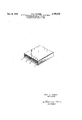
One specific embodiment of the invention is shown' partly in section and partly cut away-in theaccompanying figure.
The glass plate 1 in that embodiment carries on its surface the light-transmitting electrically-conductive layer or coating 2, in contact with the metal strip 3 which preferably extends over the corresponding edge of the glass plate 1, in the -L-shape shown. A similarL-shaped metal strip 4 is affixed to the opposite edge of the glass plate 1 as shown, it being iafiixed to a portion thereof to which the conductive-coating 2 does notextend. There is a non-conducting space between the edge of layer 2 and metal strip 4. At least part of this non-conducting space is covered by the phosphor-dielectric layer 5, which extends as a coating over the conductive layer 2, or by the dielectric coating 6 on the phosphor layer 5. The conductive backing layer 7 is applied over the dielectric layer 6, at least in part, and extends into cont-act with the metal strip 4, although it must not also extend into contact with the metal strip 3 which-is connected electrically to the transparent conductive layer 2, as that would simply short circuit the device.
The conducting surface or layer 2 should be durable, inactive chemically with respect to the other materials used in the lamp, and of good light-transmission. Such a durable, chemically-inactive conducting surface 2 of good light-transmission, either transparency or translucency, is difiicult to obtain, because good electric conductors are generally good reflectors of light, rather than transmitters of it. However, although other coatings may be used, I find that a particularly effective conductive sur- 5 of phosphorparticles embedded in dielectric. ample, in one'embodimentwe have dissolved about 3 /2 "ice face can be provided by heating the glass =andexposing it while hot to vapors of the chlorides of silicon, tin, or titanium, and afterward placingthe treated glass in a slightly reducing atmosphere. Wherethe application inthe vapor state is not convenient, good results may be obtained by mixing stannic chloride with absolute alcohol and glacial acetic acid and dipping the .heated glass plate into the boiling mixture.
The resultant conductive surface appears to be a layer 2 of stannic (or silicic or titanic) oxide, probably to some extent at least reduced to a form lower than the dioxide, although the exact composition is difficu'lt to determine.
The resistance of the conductive surface 2 should be low enough to avoid excessive power loss therein at the current used. A surface having a resistance of several hundred ohms per square, that is a resistance of several hundred ohms taken between the entire opposite edges of a square of the material, has been found satisfactory, although the permissible resistance can be varied widely.
One side of the glass plate 1 can be completely coated with the conducting layer 2, if desired, and then the portion of layer 2 in the vicinity of the position desired for the application of the metal strip 4, which must be out of electrical contact with said conducting layer 2, can be re- 'moved by applying to that portion a mixture of zinc dust mixed with sutficient zinc dust to'form a thick slurry has been found very effective.
Other methods can be used for removing a part of the conductive layer orthe original application of the layer can be confined to the desired portions by shielding or other means, if desired.
The metal strips 3 and 4 are coatings painted onto the glass piece 1 (over the conducting layer 2 in the case of strip 3) by using one of the conducting silver paints of the firing type know in the art and commonly on the market. After application, the paint is fired to the glass at about 1000 F.
Silver paints'of the 'air-dried-type can be used, but do not afford the permanent metal-to-glass bond that can be obtained with the fired paints. Spraying and other forms of metal deposition can be used instead of painting, .if
desired. A copper coating can be plated over the fired silver, for example from one of the usual acid plating If desired both contact-strips 3 and 4 may be placed along different portions of a single edge of the glass plate '1, the conductive layer 2 being in contact with the first of said strips and out of contact with the other, and
conversely, the backing layer 6 being out of contact with the first of saidcontacts 'but in contact with the second. The contact strips 3 and 4 need not extend all the way over the edge to the opposite face-8 unless desired.
The phosphor, in the form of fine particles, is suspended in asuitable dielectric medium to form the layer For exgrams of quarter-second nitrocellulose :as a dielectric material in sufficient butyl acetate to make 17 /2 cc. of the resulting solution, with about 6 /2 grams of castor oil to act as the plasticizing component of plasticizer and as the dielectric, and about 9 cc. each of toluol, ethyl acetate and butyl acetate added to thin the solution, in which about 13 grams of phosphor are suspended. The suspension is sprayed or otherwise applied to the conductive glass layer 2, to a thickness of a few thousandths of an inch.
The dielectric layer 6 can be applied in a similar manner over the phosphor-dielectric layer 5, that is by spraying, painting or the like. In the specific example described, the layer 6 was of clear lacquer applied by spraying to a thickness of about that of the phosphor-dielectric layer, although other thicknesses can be used with good results. The layer 6 should, however, be as thin as possible consistent with a good maintenance, as an extremely large thickness might reduce the luminescent brightness of the lamp for a given voltage.
The lacquer used in the specific embodiment being described was made by mixing wet quarter-second viscosity nitrocellulose equivalent to about 50 grams of dry nitrocellulose, there being about 25 grams of ethanol present to wet the material, with enough butyl acetate to make up about 250 cc. of solution. 50 grams of castor oil was added, and the resultant liquid was then diluted with about 400 cc. of a solvent of equal parts of butyl acetate, ethyl acetate, and toluol.
Caster oil is available in a wide variety of acid numbers from about down, but the best light maintenance from the lamp will be obtained with material of the very low acid numbers, less than 3 or 4.
The backing layer 7 is of a good conducting material, such as metal, and preferably of a good reflecting metal such as aluminum, which will not react appreciably with the phosphor or embedding material used. The backing layer 6 is preferably of low resistance and can be applied in any convenient manner, care being taken not to damage the phosphor-dielectric layer. Best results have been obtained by vacuum-deposition of the metal. The glass plate 1, with its conductive surface 2 coated with the embedded phosphor layer 5, is placed in a bell jar and coated over the phosphor layer 5 with an evaporated metal after a suitable vacuum has been obtained. The backing layer 7 can also be deposited effectively by spraying.
In the particular example described, the conductive backing layer 7 was an alloy of 87% aluminum and 13% copper by weight. The addition of copper to the aluminum improves the lumen maintenance of the lamp, that is, improves the maintenance of its light output during life. The addition of the copper also has the effect of greatly toughening the aluminum film and increasing its durability. Other proportions of copper and aluminum can be used than those given, but the amount of copper added should not be great enough to seriously reduce the reflectivity of the aluminum.
A transparent conductive plastic, or a transparent plastic coated with a transparent conductive layer, can be used as the piece 1, if desired. Where the piece 1 is conductive of itself, the conduction coating 2 can be omitted, but in that case the metal contact piece 4 should be separated from the piece 1 by a layer of insulation.
Other materials than nitrocellulose can be used as the embedding dielectric material, for example, a wax or plastic of reasonably high dielectric constant, dielectric strength and resistivity.
The thickness of the various layers can be altered to suit various voltage conditions and the like. The voltage will depend on the phosphor used, the thickness and composition of the layers 5 and 6, and the brightness desired, but voltages between volts and 2500 volts and even higher have been used. A lamp operable from a 110-volt alternating current power line can be made with the conducting surface 2 of a thickness of about a wavelength of light, with a phosphor layer 5 of about two one-thousandths of an inch, and a metal layer 4 of a fraction of a thousandth of an inch. The plate 1 can have any convenient thickness and must be lighttransmissive.
The phosphor used must be one capable of electroluminescence, that is of emitting light or other desired radiation on excitation by a varying electric field when the phosphor is in a dielectric medium. Suitable phosphors are described, for example, in applications, filed concurrently herewith by Keith H. Butler and Horace H. Homer as joint inventors, and by Keith H. Butler as a sole inventor, although other electroluminescent phosphors can be used.
The portion 9 of the metal backing layer 7 is preferably reinforced where it passes over the edge of the phosphor-dielectric layer 5, or the dielectric layer 6, to prevent breakage of the layer along that edge. Painting a thin stripe of one of the well-known air-drying conductive silver paints over the backing layer 7 along the portion that is in register with said edge is a satisfactory strengthening means for that portion of the lamp.
The entire back of the unit is preferably coated with an insulating protective layer 8, for example of lacquer.
What I claim is:
1. An electroluminescent lamp comprising two electrodes having therebetween a layer of an electroluminescent phosphor in a dielectric medium and a layer of dielectric material only, one of said electrodes being transparent, the other being of metal, the layer of dielectric material only being between the metal electrode and the layer containing electroluminescent phosphor, said layer of electroluminescent phosphor in a dielectric medium being homogeneous.
2. An electroluminescent lamp comprising two electrodes having therebetween a layer of an electroluminescent phosphor in a dielectric medium and a layer of dielectric material only, one of said electrodes being transparent, the other being of metal, the layer of dielectric material only being between the metal electrode and the layer containing electroluminescent phosphor, said layer of electroluminescent phosphor in a dielectric medium being homogeneous, and said layer of dielectric material only being different in composition from the dielectric in the layer of electroluminescent phosphor and dielectric medium.
References Cited by the Examiner UNITED STATES PATENTS 1,532,795 4/1925 Balch 156-67 2,733,367 1/1956 'Gilson 313108.1 2,858,632 11/1958 Casserio et a1 313108.1 2,931,915 4/1960 Jay 313108 X OTHER REFERENCES The Condensed Chemical Dictionary, Sixth Edition (1961), p. 1099.
JAMES W. LAWRENCE, Primary Examiner. GEORGE N. WESTBY, Examiner. C. R. CAMPBELL, R. L. JUDD, Assistant Exqmin ers,
Claims (1)
1. AN ELECTROLUMINESCENT LAMP COMPRISING TWO ELECTRODES HAVING THEREBETWEEN A LAYER OF AN ELECTROLUMINESCENT PHOSPHOR IN A DIELECTRIC MEDIUM AND A LAYER OF DIELECTRIC MATERIAL ONLY, ONE OF SAID ELECTRODES BEING TRANSPARENT, THE OTHER BEING OF METAL ELECTRODE AND TRIC MATERIAL ONLY BEING BETWEEN THE METAL ELECTRODE AND THE LAYER CONTAINING ELECTROLUMINESCENT PHOSPHOR, SAID LAYER OF ELECTROLUMINESCENT PHOSPHOR IN A DIELECTRIC MEDIUM BEING HOMOGENEOUS.
Priority Applications (1)
| Application Number | Priority Date | Filing Date | Title |
|---|---|---|---|
| US163758A US3290536A (en) | 1962-01-02 | 1962-01-02 | Electroluminescent lamp with homogeneous phosphor-dielectric layer |
Applications Claiming Priority (1)
| Application Number | Priority Date | Filing Date | Title |
|---|---|---|---|
| US163758A US3290536A (en) | 1962-01-02 | 1962-01-02 | Electroluminescent lamp with homogeneous phosphor-dielectric layer |
Publications (1)
| Publication Number | Publication Date |
|---|---|
| US3290536A true US3290536A (en) | 1966-12-06 |
Family
ID=22591435
Family Applications (1)
| Application Number | Title | Priority Date | Filing Date |
|---|---|---|---|
| US163758A Expired - Lifetime US3290536A (en) | 1962-01-02 | 1962-01-02 | Electroluminescent lamp with homogeneous phosphor-dielectric layer |
Country Status (1)
| Country | Link |
|---|---|
| US (1) | US3290536A (en) |
Cited By (1)
| Publication number | Priority date | Publication date | Assignee | Title |
|---|---|---|---|---|
| US5346718A (en) * | 1993-05-10 | 1994-09-13 | Timex Corporation | Electroluminescent lamp contacts and method of making of same |
Citations (4)
| Publication number | Priority date | Publication date | Assignee | Title |
|---|---|---|---|---|
| US1532795A (en) * | 1922-12-26 | 1925-04-07 | Balch Frank | Fluorescent screen and method of making same |
| US2733367A (en) * | 1956-01-31 | Electroluminescent lamp structures | ||
| US2858632A (en) * | 1955-06-27 | 1958-11-04 | Gen Motors Corp | Panel illumination |
| US2931915A (en) * | 1957-02-25 | 1960-04-05 | Sylvania Electric Prod | Electroluminescent device |
-
1962
- 1962-01-02 US US163758A patent/US3290536A/en not_active Expired - Lifetime
Patent Citations (4)
| Publication number | Priority date | Publication date | Assignee | Title |
|---|---|---|---|---|
| US2733367A (en) * | 1956-01-31 | Electroluminescent lamp structures | ||
| US1532795A (en) * | 1922-12-26 | 1925-04-07 | Balch Frank | Fluorescent screen and method of making same |
| US2858632A (en) * | 1955-06-27 | 1958-11-04 | Gen Motors Corp | Panel illumination |
| US2931915A (en) * | 1957-02-25 | 1960-04-05 | Sylvania Electric Prod | Electroluminescent device |
Cited By (1)
| Publication number | Priority date | Publication date | Assignee | Title |
|---|---|---|---|---|
| US5346718A (en) * | 1993-05-10 | 1994-09-13 | Timex Corporation | Electroluminescent lamp contacts and method of making of same |
Similar Documents
| Publication | Publication Date | Title |
|---|---|---|
| US2566349A (en) | Electroluminescent lamp | |
| US4684353A (en) | Flexible electroluminescent film laminate | |
| US4455324A (en) | Method of producing electroluminescent cell | |
| EP0830807B1 (en) | Electroluminescent lamp having a terpolymer binder | |
| US2937353A (en) | Photoconductive devices | |
| US3103607A (en) | Electroluminescent lamp with ceramic dielectric | |
| US2834903A (en) | Electroluminescent lighting device | |
| US3205393A (en) | Electroluminescent lamp with a dielectric reflective material | |
| US2894854A (en) | Electroluminescent device | |
| US3580738A (en) | Plastics materials with conductive surfaces | |
| US2911553A (en) | Electro-luminescent element | |
| US3421037A (en) | Electroluminescent device and dielectric medium therefor | |
| US3290536A (en) | Electroluminescent lamp with homogeneous phosphor-dielectric layer | |
| US3043978A (en) | Electroluminescent lamp | |
| JPH0878164A (en) | Conductive paste, translucent conductive film, and dispersed electroluminescence device using the same | |
| US3346758A (en) | Electroluminescent lamp having an aluminum electrode with an aluminum oxide layer disposed between the aluminum electrode and the electroluminescent material | |
| US3104339A (en) | Electroluminescent device | |
| US3154712A (en) | Electroluminescent lamp | |
| US2966604A (en) | Electroluminescent lamp | |
| US3048732A (en) | Electroluminescent cell | |
| US3044902A (en) | Method of forming films of electro-luminescent phosphor | |
| US3073982A (en) | Electroluminescent device | |
| US3143682A (en) | Electroluminescent devices with a barium titanate layer | |
| US2848637A (en) | Electroluminescent lamp | |
| US3346757A (en) | Electroluminescent lamp having an aluminum electrode, a layer of di-electric material and an aluminum oxide layer disposed between the aluminum electrode and the dielectric layer |