Dec. 6, 1966 T. v. RYCHLEWSKI 3,290,531
ELECTRONIC SWITCHING TUBE Filed July 1 1963 2 Sheets-Sheet 1 F29 n INVENTOR Thaddeus l4 Rych/en sk/ ATTORNEY Dec. 6, 1966 T. v. RYCHLEWSKI ELECTRONIC SWITCHING TUBE Filed July 1, 1963 2 Sheets-Sheet 2 INVENTOR Thaddeus I! Kych/ewsk/ ATTORN EY United States Patent 3,290,531 ELECTRUNIC SWITCHING TUBE Thaddeus V. Rychlewski, Seneca Falls, N.Y., assignor to Sylvania Electric Products llnc., a corporation of Dela- Ware Filed July l, 1963, Ser. No. 291,665 Claims. (Cl. 3I369) This invention generally relates to electron discharge devices and more particularly to an electronic switching tube capable of converting an input signal of a given code to an output signal of a different form or code.
In the prior art, to accomplish the function of switching from one code system to another, it was necessary to utilize a multiplicity of either diodes, transistors, or vacuum tubes, or else where a single vacuum tube was used, to utilize a multiplicity of built-in stacked control grids to control the passage of an electron flow from a cathode to a selected anode or anodes therein.
It is an object of the invention to provide improved and simplified electronic switching for effecting code conversion functions.
It is another object of this invention to provide simple and improved means for translating electrical impulses into a visual readout.
Another object of this invention is the provision of an electronic switching device that is less costly to manufacture than those used heretofore.
These and other objects are achieved in one aspect of the invention by the provision of an electronic switch ing tube comprising a cathode or source of electron emission, a grid or gating structure, and a plurality of anodes so arranged that selective modulation of the gating structure will cause electron impingement upon one or more anodes, thereby completing one or more circuits and allowing switching functions to be performed.
This tube provides many advantages over the prior art. It is a completely self-contained unit and therefore obviates the necessity of using a multiplicity of diodes or transistors. It can be used as a translator for visual readout devices, and it is relatively inexpensive to make.
For a better understanding of the present invention, together with other and further objects, advantages, and capabilities thereof, reference is made to the following disclosure and appended claims in connection with the accompanying drawings in which:
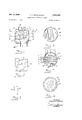
FIG. 1 is a sectional elevational view of a vacuum tube illustrative of the principles involved;
FIG. 2 is a sectional view taken along the line 2-2 of r FIG. 1;
FIG. 3 is a sectional view taken along the line 33 of FIG. 1;
FIG. 4 is a sectional view taken along the line 44 of FIG. 1;
FIG. 5 is a diagrammatic representation of a visual display board that may be utilized in one aspect of the invention;
FIG. 6 is a simplified schematic view of an anode connection; and
FIG. 7 is a cross-sectional view of a modified form of the invention.
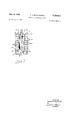
Referring now to the drawings with greater particularity, in FIG. 1 there is shown an electronic switch- 3,29%,531 Patented Dec. 6, I966 ice ing tube designated generally as 10 comprised of an insulating envelope 11, as of glass, encapsulating a cathode or source of electron emission 12, a grid or gating structure 14, and an anode or target assembly 16. The cathode may comprise a cylindrical ceramic slab 18 with embedded heater 2t and can be coated on its upper face wit-h a thin metallic film 22 which is in turn coated with electron emissive material 24. Spaced from the cathode is gating structure 14 comprised of an insulating disc 26, such as of mica or ceramic. The disc has parallel rows of perforations 28 formed therein to allow the passage of electrons therethrough. The electrons are drawn from cathode 12 by the electric field created by target 16 during tube operation.
The perforations of each row are connected together by conductive strips, indicated generally as 30, FIG. 3, applied to the surface of ceramic 26 in any conventional fashion; and preferably the conductive material surrounds the cylindrical walls of perforations 28. The perforations 28 in each strip are arranged in position and number in accordance with a selected code as will be later explained in detail. Spaced from the gating structure 14 is the target assembly 16 shown in FIG. 2. This assembly may comprise an insulating disc 32 with a series of parallel spaced conductors, such as bars 34 therebeneath. Bars 34 lie in a plane parallel to gating structure 14 and at an angle, preferably at a right angle, to the rows of perforations 28. The bars 34 each terminate in a connecting pin 36 exteriorly of the tube and pins 36 are in turn electrically connected to a B+ supply through load 37 as is shown schematically in FIG. 6.
One typical example of tube application is where the tube is designed to convert decimal information into a numeric display on a support and wherein all of the numeric designations may be represented by suitable selection of any one or more of seven elongated lights, such as incandescent lamps. In this instance, the matrix within the switching tube would consist of a grid with ten rows of perforations, one row for each digit 0-9, and the anode would consist of seven spaced bars. In FIG. 5 there is illustrated a numeric display board 40 with seven lamps, A, B, C, D, E, F, and G, energized in accordance with the energization of the terminals 36 of the tube.
It will be seen that in this instance, the lamps A-G each cor-respond to a load 37, only one of which is shown in FIG. 6, and that they are connected at one side to a pin 36 and at the other side to a common source of B+.
Obviously, other arangements can be made within the scope of the invention, as for example, the tube could be designed so that there are (n) anodes coupled to (11) supplies of B+ controlling (n) circuits.
In FIG. 3 there is shown a typical matrix 42 illustrating the switching action of electron tube lid. The vertical lines indicated as a, b, c, d, e, f, g represent the seven anode bars 34, while the horizontal lines labeled 0, 1, 2, 3, 4, 5, s, 7, 8, and 9 represent the gating strips 30'. If, for example, it is desired to indicate 0 on the numeric representation board 40, the il strip in FIG. 3 would have a positive potential imposed thereon relative to the cathode potential. This strip controls the electron flow, as shown in FIG. 3, through six apertures directly aligned with bars a, b, c, e, f, and g. As electrons flow through the designated apertures, they cause the corresponding lamps A, B, C, E, F, and G to be energized and the numer- .3 al to appear on the board 40. If the numeric value 3 be imposed on the gating structure of the tube, the 3 strip would have a positive potential imposed thereon. Since this strip controls five apertures opposed to bars corresponding to lines a, c, d, f, and g, the numeral 3 will appear on the numeric display board. All of the strips 30 of gating structure 14, as well as the heater and cathode leads, are led to suitable pins 44 extending through the wafer base of the tube. The leads 36 conveniently may be extended through the bulb end of the tube; however, this is a matter of choice and other arrangements may be equally suitable.
It will be obvious that if enough conductive strips 30 and bars 34 are provided in the matrix within the tube, and a suitable number of lamps are provided, the display on the board 40 could be an alpha-numeric presentation as well as the numeric presentation illustrated.
Also, by providing ten bars 34 instead of seven and suitably perforating the strips 30, one hole opposite to and for each bar 34, the connections 36 may control the illumination of any one or more characters in the form of digital numbers 0-9.
It will be apparent to those skilled in the art that, while the invention has been described as utilizing a visual readout device, other applications will work equally well. For example, as stated above, there could be (11) sources of supply of B+ through (It) loads which need not be lamps but may be relays or motors or like devices controlling (n) different circuits.
In a modified form of the invention, see FIG. 7, the disc type cathode of FIG. 1 is replaced by a metallic cathode sleeve 60 supported between a pair of insulating spacers 61, as of mica. The sleeve is coated with a film of electron emissive material 62 and is symmetrically surrounded by an insulating sleeve 64, as of a ceramic material which is also supported between spacers 61. The sleeve 64 is perforated, as at 66, at selected horizontal elevations along its length and along lines parallel to its longitudinal vertical axis. The walls of the perforations 66 are preferably coated with an electrically conductive coating and they are connected to conductive strips 68, all corresponding to the organization of FIG. 3, and terminating in terminal pins 70 at the endof encapsulating insulating envelope 72. In the cross-sectional view of FIG. 7 two rows of holes 66 are shown corresponding to the numeric values 0 and 4.
Surrounding the ceramic sleeve 64 at each horizontal level of holes is an anode ring 74 which terminates in a pin 78 leading out of the side of the bulb or envelope 72.
When cathode beam electrons are accelerated by a suitable potential, positive with respect to cathode, being applied to a strip 68 on sleeve or gate structure 64, it will strike the appropriate anode rings 74 thereby completing an energy circuit via rings 74 and pins 78 to operate a readout device on other apparatus.
This invention, therefore, provides a simple and improved electronic switching tube that is useful for effecting code conversions. It can be used as a translator for visual readout devices, and it is relatively inexpensive to make. Also, because of the fact that it is self-contained, even more cost savings are acquired over the multiplicity of prior art systems.
While there have been shown and described what are at present considered the preferred embodiments of the invention, it will be obvious to those skilled in the art that various changes and modifications may be made therein wtihout departing from the invention as defined by the appended claims.
What is claimed is:
1. An electronic switching tube comprising a source of electron emission, means accelerating electrons emitted from said source and anode bars on which the electrons impinge, said electron accelerating means comprising a gating structure with parallel lines of perforations therein, the perforations being spaced in rows in accordance with a desired code, with the arrangement of perforations in one row different from that in any other row, and said anode bars lying in a plane parallel to and spaced from said gating structure, said bars in said plane being at an angle to said rows of perforations in said gating structure, conductor means connecting together said rows of perforations, one for each row, and lead-in means for each conductor and for the bars.
2. An electronic switching tube comprising a source of electron emission, a target assembly toward which the electrons are directed and a gating structure therebetween, said gating structure comprising an electrically insulating support having parallel rows of apertures therethrough, a number of apertured conductive means overlying said apertures in said support for controlling the flow of electrons therethrough, said apertures in said conductive means being aligned with said apertures in said support, and said target assembly comprising conductors traversing all of the conductive means of said gating structure, and individual connections leading to each of the conductive means and connections to the source of electron emission and the conductors of the target assembly.
3. An electronic switching tube comprising an insulating envelope, a flat cathode therein, a fiat gating structure spaced from said cathode and parallel thereto, said structure having parallel rows of perforations therethrough wit-h perforations in one row arranged in spacing and number different from .any other row, conductive strips, one for each row of perforations in said structure, along the length of row of perforations, said strips being apertured at said perforations, and a fiat target spaced from said gating structure, said target having parallel bars arranged crosswise of the rows of perforations in said gating structure, and lead-in pins extending through said envelope and connected respectively with the cathode, the conductive strips, and the bars.
4. An electronic switching tube comprising an insulating envelope encapsulating a cathode, gating structure, and target assembly all spaced from each other, said gating structure comprising an insulating support with parallel rows of holes therein, conductive lining material on the walls of the holes in the support and conductive strips interconnecting the lining material, one strip for each row of holes, said target assembly comprising parallel bars insulatively supported one from the other, all of said bars being arranged transverse to the strips and of an extent to cross all of the strips and in substantial alignment with holes therein, lead-in pins extending through said envelope and individual connections from said pins to said cathode, the strips on the gating structure and the parallel bars.
5. A mount for a switching tube comprising a cathode, a nonconductive sleeve surrounding the cathode, said sleeve having rows of perforations therein arranged peripherally about the sleeve and at spaced elevations along the sleeve, grids connected to each row of perforations, and anode rings surrounding the grids and spaced therefrom, said anode rings extending transversely to said crossing all of the grids.
6. An electronic switching tube comprising an insulating evacuated envelope encapsulating an electron tube mount comprising a pair of insulating spacers, a cylindrical cathode support therebetween, a nonconductive sleeve supported between said spacers and surrounding said cathode, said sleeve having rows of perforations therein arranged peripherally about the sleeve and at spaced elevations along the sleeve, conductive strips running longitudinally of the sleeve connecting the perforations and perforated at said perforations, and anode rings at spaced elevations about the sleeve, the vertical rows of perforations being so arranged that when one does exist in the sleeve it will be substantially opposite a ring.
7. A mount for a switching tube comprising a cathode, a nonconductive sleeve surrounding the cathode, said sleeve having rows of perforations therein arranged longitudinally of the sleeve and at spaced angular distances about the sleeve, conductive strips running longitudinally of the sleeve connecting the perforations and perforated at said perforations, and anode rings at spaced elevations about the sleeve, the vertical rows of perforations being so arranged that When one does exist in the sleeve it will be substantially opposite a ring.
8. A mount for a switching tube comprising a pair of insulating spacers, a cathode supported therebetween, a nonconductive sleeve supported between the spacers and surrounding the cathode, said sleeve having rows of perforations therein arranged longitudinally of the sleeve and at spaced angular distances about the sleeve, condnc tive strips running longitudinally of the sleeve along the rows of perforations and perforated at said perforations, and rings at spaced elevations about the sleeve, the vertical rows of perforations being so arranged that when one does exist in the sleeve it will be substantially opposite a ring.
No references cited.
JAMES W. LAWRENCE, Primary Examiner.
V. A. LAFRANCHI, Assistant Examiner.