US2114613A - Cathode ray tube - Google Patents
Cathode ray tube Download PDFInfo
- Publication number
- US2114613A US2114613A US754710A US75471034A US2114613A US 2114613 A US2114613 A US 2114613A US 754710 A US754710 A US 754710A US 75471034 A US75471034 A US 75471034A US 2114613 A US2114613 A US 2114613A
- Authority
- US
- United States
- Prior art keywords
- bundle
- electron
- anode structure
- cathode
- anode
- Prior art date
- Legal status (The legal status is an assumption and is not a legal conclusion. Google has not performed a legal analysis and makes no representation as to the accuracy of the status listed.)
- Expired - Lifetime
Links
Images
Classifications
-
- H—ELECTRICITY
- H01—ELECTRIC ELEMENTS
- H01J—ELECTRIC DISCHARGE TUBES OR DISCHARGE LAMPS
- H01J31/00—Cathode ray tubes; Electron beam tubes
- H01J31/02—Cathode ray tubes; Electron beam tubes having one or more output electrodes which may be impacted selectively by the ray or beam, and onto, from, or over which the ray or beam may be deflected or de-focused
- H01J31/04—Cathode ray tubes; Electron beam tubes having one or more output electrodes which may be impacted selectively by the ray or beam, and onto, from, or over which the ray or beam may be deflected or de-focused with only one or two output electrodes with only two electrically independant groups or electrodes
-
- H—ELECTRICITY
- H03—ELECTRONIC CIRCUITRY
- H03B—GENERATION OF OSCILLATIONS, DIRECTLY OR BY FREQUENCY-CHANGING, BY CIRCUITS EMPLOYING ACTIVE ELEMENTS WHICH OPERATE IN A NON-SWITCHING MANNER; GENERATION OF NOISE BY SUCH CIRCUITS
- H03B13/00—Generation of oscillations using deflection of electron beam in a cathode-ray tube
Definitions
- This invention relates to electron tubes for amplifying and like purposes.
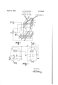
- Fig. 1 is a perspective view of the electrode system of an electron tube acting on the so-called transverse field principle and designed according to the invention
- Fig. 2 is a sectional view of the same system, both said figures showing some essential circuit elements too.
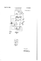
- Fig. 3 shows a special embodiment of partanodes of the tube in plan view
- Fig. 4 there is illustrated an additional feature of the invention consisting in the cascade connection of a plurality of tubes according to the invention.
- the arrangement comprises a straight cathode filament l of, say, 40 mm. in length, which is arranged within a sheet metal box-like structure 2.
- a. sectional anode 3 having a wide aperture, behind this anode a further box 4, and behind the latter an anode having a very narrow aperture 5.
- the potentials hereinafter recited are to be understood relatively to cathode potential as zero potential.
- the box 2 and the box 4 are connected to a potential not considerably different from zero, or with suitable dimensioning, are connected with zero potential itself, and the anodes 3 and 5 are on the other hand connected with a potential of 200 volts, it is possible to cause practically all of the electrons emitted by l to pass through the diaphragm aperture of 5 with a. comparatively small angle of dispersion and reach the deflecting space situated behind the same.
- all of the stated electrode potential may also be regulated separately.
- the two deflecting plates 6 and I which are, for example, approximately 40 mm. high.
- the tube according to the invention is preferably of the high vacuum type.
- the tube may be connected as follows:
- An anode battery l2 of approximately 200 volts is connected with its positive pole not only with the preliminary anodes 3 and 5, but also with the upper box 9, and with its negative pole with 5 the filament I and the concentration electrodes 2 and 4 connected therewith.
- a part potential tapped from this anode battery is linked up "with the lower box electrode 8.
- this component potential is earthed externally, directly earthed (earth l3).
- One of the deflecting plates, for example the plate 6, is connected with the source ll of the voltage to be amplified, the other pole of which source is practically always earthed.
- the plate 7, according to the invention, is earthed over a potentiometer l5 at a tapping l6, whilst the free pole of the potentiometer I5 is connected with the anode l0 through the medium of the blocking condenser Ill.
- the anode Ill receives a bias via the resistance l9, which should be high as compared with IS in respect of all frequencies employed.
- the anode II is earthed as regards alternating current over a working resistance 26 and condenser I1.
- the two anodes receive a d. c. bias from the battery l2, it being with suitable dimensioning also possible to operate the tube with a bias which coincides with the earth potential l3.
- an electrostatic electron-optical reproduction on a scale which, as in the optical art, may be calculated from the distance between the object to be reproduced (i. e. the aperture in 5) and the line of intersection of 8-9 on the one hand and the distance between that line of intersection and the image (in the plane Ill-H) on the other hand.
- the first mentioned distance is approximately 50 mm.
- the ring 8 approximately 10 mm.
- the upper guard ring 9 approximately 20 mm. high, so that the image is approximately half as wide as the aperture of 5, and in practice with an aperture .5 mm. in width merely an electronic image of .25 mm. in width is projected on to the anodes l0 and II. A filling of gas is unnecessary.
- the oscillating voltage II to be amplified causes this electronic image to oscillate laterally, and thus to sweep over the line of separation shown in Figs. 1 and 3 between the two part-anodes I0 and II. It is possible, therefore, to obtain at the anode II a potential corresponding in its phase to the voltage l4 and being amplified in relation to I by a factor which is proportional to the slope tan a (Fig. 3).
- the lower ring 8 has the object of screening off the electrostatic refractive edge 2
- the diameters of 8 and 9 are further selected to be so much larger than the maximum extent of movement on the part of the cathode ray that the reproduction remains uniformly sharp even at the edge.
- the distance of the object to be electron optically reproduced from the reproducing lens may be selected to be relatively large, and the two anodes l0 and I I may then be connected with earth.
- the measure according to the invention enables difierent extremely effective connections to be performed.
- the circuit anode I0 is, as regards alternating currents, connected over l8 with the plate I, provision being made for ad- ;lustability of the degree of this coupling by the tapping ii. In this manner, as quite readily apparent, the oscillation amplitude is considerably increased.
- the degree of back-coupling may be increased to such an extent in accordance with the invention that the ray is capable of assuming merely two positions of deflection, which remain stable. Since the ray is thrown suddenly from the one to the other position as soon as the potential ll exceeds a certain amount, an arrangement of this nature is very suitable as a tilting relay dependent on a threshold value, and may with advantage be employed in all circuits known for this purpose, for example, as a substitute for the Turner callirotron, which is an oscillator comprising two valves, in which a negative resistance effect is obtained in the anode circuit of the second valve, and in which the grid of the second valve is connected to the anode circuit of the first valve and the anode circuit of the second valve connected to the grid circuit of the first valve.
- the Turner callirotron which is an oscillator comprising two valves, in which a negative resistance effect is obtained in the anode circuit of the second valve, and in which the grid of the second valve is connected to the anode circuit
- An additional feature of the invention consists in the cascade connection of a plurality of these tubes (Fig. 4). For simplicitys sake there are shown of these tubes merely the diaphragms 5, the deflecting plates 6 and I and the two anodes l0 and H.
- the first tube is operated by the potential source I4 in the back-coupling connection above described increasing the amplification aperiodically. Amplified potential fluctuations are then obtained at the anodes III and H, those obtained at ll having the same phase .as, those obtained at l0 having a phase reversed in relation to, the input voltage fluctuations.
- the output of the first tube is coupled to the input of the second one.
- This coupling may be effected in single phase by providing only one connection, such as the wire 22, between the first and second tubes.
- the said coupling is preferably effected by a push-pull connection employing two wires 22 and 23.
- the sensitivity of pushpull cathode ray deflection is, other data being equal, twice the sensitivity of single phase cathode ray deflection.
- the amplification per stage obtained by the push-pull coupling is accordingly doubled in relation to that obtained by single phase coupling.
- the output potentials may be taken from the anodes l0 and I I of the final tube in opposite phases, and under certain circumstances, therefore, may be doubled by the use of a counter-cadence transformer 24, even if this possesses the transformation ratio 1.
- the sensitiveness of the second tube may also be increased by the use of 2. preferably aperiodic back-coupling in the same manner as described in connection with the first tube. This is particularly advisable in those cases in which, due to wide frequency bands, the use of transformers is made diificult, for example in certain amplifier circuits for teevision purposes.
- the circuit shown in Fig. 4 may, since it is possible in accordance with the invention to avoid block condensers in the train of the lines 22, 23, be employed as an effective d. c. amplifier.
- the condition in question may be fulfilled either by so dimensioning the distance of the anodes from the other parts of the electrode system in the tubes in Figs. 1 and 2 that the anodes ill and II may be directly connected with earth, or this condition may also be fulfilled by correspondingly increasing from stage to stage the battery potential of the tubes.
- An electron tube comprising means including a cathode for producing a bundle of electrons, at least one anode structure comprising at least one equipotential element, electron optical means comprising a plurality of electrodes consecutively mounted along the direction from said cathode to said anode structure for producing in the space between said cathode and said anode structure an electron-optical lens field for forming said bundle into a sharp electron image in the plane of said anode structure, a wire net mounted between said anode structure and the adjacent one of said electrodes, and connected with the last mentioned electrode, further electron-optical means mounted more remote from said anode structure than the first said electron-optical means for substantially parallelizing said bundle, and electron deflecting means mounted between said cathode and said anode structure for deflecting said bundle of electrons to a variable degree to cause the percentage of electrons impinging on any of said equipotential elements to be variable in dependence on the variations in the degree to which said bundle'is deflected.
- An electron tube for producing electrically influenced currents comprising means including a cathode for producing a bundle of electrons, an anode structure comprising at least one equipotential element, electron optical means mounted between said cathode and said anode structure for producing an electron optical lens field for forming said bundle into a sharp electron image in the plane of said anode structure, further electron optical means, mounted more remote from said anode structure than the first said electron optical means, for substantially parallelizing said bundle, and electron deflecting means mounted between said cathode and said anode structure for deflecting said bundle of electrons to a variable degree to cause the percentage of electrons impinging on any of said equipotential elements to be variable in dependence on the variations in the degree to which said bundle is deflected.
- An electron tube for producing electrically influenced currents comprising means including a cathode having an emissive surface the width of which is small as compared with its length for producing a bundle of electrons, an anode structure comprising at least one equipotential element having an edge which is sloped with respect to the main direction of said emissive surface, electron optical means mounted between said cathode and said anode structure for producing an electron optical lens field for forming said bundle into a sharp electron image in the plane of said anode structure, further electron optical means, mounted more remote from said anode structure than the first said electron optical means, for substantially parallelizing said bundle, and electron deflecting means mounted between said cathode and said anode structure for deflecting said bundle of electrons to a variable degree in a direction forming right angles with the main direction of said emissive surface to cause the percentage of electrons impinging on any of said equipotential elements to be variable in dependence on the variations in the degree to which said bundle is deflected.
- An electron tube for producing electrically influenced currents comprising means including a cathode having an emissive surface the width of which is small as compared with its length, for producing a bundle of electrons, an anode structure formed by a plate-shaped element mounted at right angles to the normal path of said bundle and separated into two equipotential elements insulated from each other by a slot disposed at an acute angle with respect to the main direction of said emissive surface, electron optical means mounted between said cathode and said anode structure for producing an electron optical lens field for forming said bundle into a sharp electron image in the plane of said anode structure, further electron optical means mounted more remote from said anode structure than the first said electron optical means for substantially parallelizing said bundle, and electron deflecting means mounted between said cathode and said anode structure for deflecting said bundle of electrons to a variable degree in a direction forming right'angles with the main direction of said emissive surface to cause the percentage of electrons impinging in any of said
- An electron tube for producing electrically influenced currents comprising means including a cathode for producing a bundle of electrons, an anode structure comprising at least one equipotential element, a diaphragm having an aperture positioned in the path of said bundle between said cathode and said anode structure, electron optical means mounted between said diaphragm and said anode structure for producing an electron optical lens fleld for forming said bundle into a sharp electron image of said diaphragm aperture in the plane of said anode structure, further electron optical means, mounted more remote from said anode structure than said diaphragm, for substantially parallelizing said bundle, and electron deflecting means mounted between said diaphragm and said anode structure for deflecting said bundle of electrons to a variable degree to cause the percentage of electrons impinging on any of said equipotential elements to be variable in dependence on the variations in the degree to which said bundle is deflected.
- An electron tube for producing electrically influenced currents comprising means including a cathode having an emissive surfacethe width of which is small as compared with its length for producing a bundle of electrons, an anode structure comprising at least one equipotential element, a diaphragm having a very narrow aperture similar in shape and disposed in parallel to said emissive surface positioned in the path of said bundle between said cathode and said anode structure, electron optical means mounted between said diaphragm and said anode structure for producing an electron optical lens fleld for forming said bundle into a sharp electron image of said diaphragm aperture in the plane of said anode structure, further electron optical means mounted more remote from said anode structure than said diaphragm, for substantially parallelizing said bundle, and electron deflecting means mounted-between said diaphragm and said anode structure for deflecting said bundle oi. electrons elements to be variable in dependence on the variations in the degree to which said bundle is deflected.
- said further electron optical means comprise two plane rectangular metal sheets mounted in parallel to each other and to the normal path of said bundle and flanking said bundle from opposite sides thereof.
- said further electron optical means comprise two plane rectangular metal sheets mounted in parallel to each other and to the normal path of said bundle and fianking said bundle from opposite sides thereof, and two further plane rectangular metal sheets supplementing the two first said sheets to form a box-like structure.
- the first said electron optical means comprise two pairs of plane rectangular metal sheets mounted in parallel to each other and to the normal path of said bundle, the sheets of each of said pair flanking said bundle from opposite sides thereof, said two pairs being mounted to follow one on the other in the direction of the normal path of said bundle and being adapted to have different potentials impressed thereo 12.
- first said electron optical means comprise two pairs of plane rectangular metal sheets mounted in parallel to each other and to the normal path of said bundle, the sheets of each of said pairs flanking said bundle from opposite sides thereof, said two pairs being mounted to follow one on the other in the direction of the normal path of said bundle and being adapted to have different potentials impressed thereon, and two further pairs of plane rectangular metal sheets, each of said further pairs supplementing one of the first said pairs to form a box-like structure.
- said deflecting means are deflecting plates
- the first said electron optical means comprise two pairs of plane rectangular metal sheets mounted in parallel to each other and to the normal path of said bundle, the sheets of each of said pairs flanking said bundle from opposite sides thereof, said two pairs being mounted to follow one on the other in the direction of the normal path of said bundle and being adapted to have different potentials impressed thereon.
- said deflecting means are deflecting plates, mounted more remote from said anode structure than the first said electron optical means, wherein the first said electron optical means comprise two pairs of plane rectangular metal sheets mounted in parallel to each other and to the normal path of said bundle, the sheets of each of said pairs flanking said bundle from opposite sides thereof, said two pairs being mounted to follow one on the other'in the direction of the normal path of saidburidle and being adapted to have different potentials impressed thereon, and wherein that one of said pairs mounted never said deflecting plates is generously dimensioned in the direction parallel to the normal path of said bundle, so that this last mentioned pair screens the lens field produced by the first said electron optical means from said deflecting plates.
- said deflecting means are deflecting plates
- the first said electron optical means comprise two pairs of plane rectangular metal sheets mounted in parallel to each other and to the normal path of said bundle, the sheets of each of said pairs flanking said bundle from opposite sides thereof, said two pairs being mounted to follow one on the other in the direction of the normal path of said bundle and being adapted to have different potentials impressed thereon, and two further pairs of plane rectangular metal sheets, each of said further pairs supplementing one of the first said pairs to form a box-like structure
- said further electron optical means comprise "a pair of plane rectangular metal sheets mounted in parallel to each other and to the normal path of said bundle and flanking said bundle from opposite sides thereof, and yet a further pair of plane rectangular metal sheets supplementing the aforementioned pair incorporated in said further electron optical means to form a box-like structure
- said deflecting plates are likewise provided with supplementary metal members to give them a box-like structure as well, so that the complete path of said bundle is electro-statically screened towards the
Description
April 19, 1938. K. SCHLESINGER CATHODE RAY TUBE Filed Nov. 26. 1934 2 Sheets-Sheet l 7/? 126/? foe: MET/m? April 19', 1938.
GATHODE RAY TUBE Filed Nov. 26, 1954 2 Sheets-Sheet 2 K. SCHLESINGER ,613
Patented Apr. 19, 1938 UNITED STATES PATENT OFFICE Application November 26, 1934, Serial No. 754,710 In Germany November 27, 1933 16 Claims.
This invention relates to electron tubes for amplifying and like purposes.
The invention will be best understood with reference to the accompanying drawings of which Fig. 1 is a perspective view of the electrode system of an electron tube acting on the so-called transverse field principle and designed according to the invention, whereas Fig. 2 is a sectional view of the same system, both said figures showing some essential circuit elements too.
Fig. 3 shows a special embodiment of partanodes of the tube in plan view, while in Fig. 4 there is illustrated an additional feature of the invention consisting in the cascade connection of a plurality of tubes according to the invention.
In particular referring to Fig. l the arrangement comprises a straight cathode filament l of, say, 40 mm. in length, which is arranged within a sheet metal box-like structure 2. In front of the sheet metal structure 2 there is situated a. sectional anode 3 having a wide aperture, behind this anode a further box 4, and behind the latter an anode having a very narrow aperture 5. The potentials hereinafter recited are to be understood relatively to cathode potential as zero potential. If the box 2 and the box 4 are connected to a potential not considerably different from zero, or with suitable dimensioning, are connected with zero potential itself, and the anodes 3 and 5 are on the other hand connected with a potential of 200 volts, it is possible to cause practically all of the electrons emitted by l to pass through the diaphragm aperture of 5 with a. comparatively small angle of dispersion and reach the deflecting space situated behind the same. Naturally in accordance with the invention all of the stated electrode potential may also be regulated separately. In the deflecting space there are situated the two deflecting plates 6 and I which are, for example, approximately 40 mm. high. Behind these there is located a box shaped electrode 8, and then an additional box shaped electrode 9, and finally two anodes l0 and H. The latter are shown in plan view in Fig. 3. In the practical form of embodiment of the tubes all electrodes are conveniently closed oil by metal parts towards the front and the rear, so that the entire tube is given a box-like structure, in such a manner that the electronic path is completely screened off towards the outside.
The tube according to the invention is preferably of the high vacuum type.
The tube may be connected as follows:
An anode battery l2 of approximately 200 volts is connected with its positive pole not only with the preliminary anodes 3 and 5, but also with the upper box 9, and with its negative pole with 5 the filament I and the concentration electrodes 2 and 4 connected therewith. A part potential tapped from this anode battery is linked up "with the lower box electrode 8. Preferably this component potential is earthed externally, directly earthed (earth l3). One of the deflecting plates, for example the plate 6, is connected with the source ll of the voltage to be amplified, the other pole of which source is practically always earthed. The plate 7, according to the invention, is earthed over a potentiometer l5 at a tapping l6, whilst the free pole of the potentiometer I5 is connected with the anode l0 through the medium of the blocking condenser Ill. The anode Ill receives a bias via the resistance l9, which should be high as compared with IS in respect of all frequencies employed. The anode II is earthed as regards alternating current over a working resistance 26 and condenser I1. The two anodes receive a d. c. bias from the battery l2, it being with suitable dimensioning also possible to operate the tube with a bias which coincides with the earth potential l3. Under certain circumstances this may be accomplished by the provision of a coarse-mesh net 9a in front of the anode connected with 9, or by increase of the length of 9, whereby there is certainly obtained a wider electronic image, but on the other hand a greater sensitiveness of deflection in mm. per volt. In the latter case the condenser l8 and the feeding resistance l9 and the condenser I'I may also be dispensed with. The amplified potential is taken through the medium of a block 20.
The operation of an arrangement of this nature is as follows:
The aperture of 5 onto which an intense electron stream is projected by means of the concentrating device I, 2, 3, 4, as described above, is reproduced sharply on the plane of the anodes l0 and II. This reproduction is obtained by the fact that the lower system: deflecting plates 6 and i and guard screen 8 are connected in common with a less high positive bias than the upper system 9 and possibly l0 and II. In consequence there are formed at the line of intersection between 9 and 8 potential lines of the form as shown in broken lines and designated 2| in Fig. 2. This combination already described by the applicant on a previous occasion provides .55'
an electrostatic electron-optical reproduction on a scale which, as in the optical art, may be calculated from the distance between the object to be reproduced (i. e. the aperture in 5) and the line of intersection of 8-9 on the one hand and the distance between that line of intersection and the image (in the plane Ill-H) on the other hand. In the stated tube the first mentioned distance is approximately 50 mm., and the ring 8 approximately 10 mm. and the upper guard ring 9 approximately 20 mm. high, so that the image is approximately half as wide as the aperture of 5, and in practice with an aperture .5 mm. in width merely an electronic image of .25 mm. in width is projected on to the anodes l0 and II. A filling of gas is unnecessary. The oscillating voltage II to be amplified causes this electronic image to oscillate laterally, and thus to sweep over the line of separation shown in Figs. 1 and 3 between the two part-anodes I0 and II. It is possible, therefore, to obtain at the anode II a potential corresponding in its phase to the voltage l4 and being amplified in relation to I by a factor which is proportional to the slope tan a (Fig. 3). The lower ring 8 has the object of screening off the electrostatic refractive edge 2| against the variable field between 6 and I. The diameters of 8 and 9 are further selected to be so much larger than the maximum extent of movement on the part of the cathode ray that the reproduction remains uniformly sharp even at the edge.
In accordance with the invention, the distance of the object to be electron optically reproduced from the reproducing lens may be selected to be relatively large, and the two anodes l0 and I I may then be connected with earth.
The measure according to the invention enables difierent extremely effective connections to be performed.
In order to increase the amplification beyond the product of working resistance 26 and steepness it is possible, for example, to employ the following galvanic back-coupling according to the invention: The circuit anode I0 is, as regards alternating currents, connected over l8 with the plate I, provision being made for ad- ;lustability of the degree of this coupling by the tapping ii. In this manner, as quite readily apparent, the oscillation amplitude is considerably increased.
The degree of back-coupling may be increased to such an extent in accordance with the invention that the ray is capable of assuming merely two positions of deflection, which remain stable. Since the ray is thrown suddenly from the one to the other position as soon as the potential ll exceeds a certain amount, an arrangement of this nature is very suitable as a tilting relay dependent on a threshold value, and may with advantage be employed in all circuits known for this purpose, for example, as a substitute for the Turner callirotron, which is an oscillator comprising two valves, in which a negative resistance effect is obtained in the anode circuit of the second valve, and in which the grid of the second valve is connected to the anode circuit of the first valve and the anode circuit of the second valve connected to the grid circuit of the first valve. A description of this device is for instance to be found in Scott-Taggarts book on Thermionic Tubes", second edition, published from the ofiices of The Wireless World" on page 416.
An additional feature of the invention consists in the cascade connection of a plurality of these tubes (Fig. 4). For simplicitys sake there are shown of these tubes merely the diaphragms 5, the deflecting plates 6 and I and the two anodes l0 and H. The first tube is operated by the potential source I4 in the back-coupling connection above described increasing the amplification aperiodically. Amplified potential fluctuations are then obtained at the anodes III and H, those obtained at ll having the same phase .as, those obtained at l0 having a phase reversed in relation to, the input voltage fluctuations.
The output of the first tube is coupled to the input of the second one. This coupling may be effected in single phase by providing only one connection, such as the wire 22, between the first and second tubes. According to a further feature of the invention, however, the said coupling is preferably effected by a push-pull connection employing two wires 22 and 23. The sensitivity of pushpull cathode ray deflection is, other data being equal, twice the sensitivity of single phase cathode ray deflection. The amplification per stage obtained by the push-pull coupling is accordingly doubled in relation to that obtained by single phase coupling. The output potentials may be taken from the anodes l0 and I I of the final tube in opposite phases, and under certain circumstances, therefore, may be doubled by the use of a counter-cadence transformer 24, even if this possesses the transformation ratio 1. Naturally the sensitiveness of the second tube may also be increased by the use of 2. preferably aperiodic back-coupling in the same manner as described in connection with the first tube. This is particularly advisable in those cases in which, due to wide frequency bands, the use of transformers is made diificult, for example in certain amplifier circuits for teevision purposes.
The circuit shown in Fig. 4 may, since it is possible in accordance with the invention to avoid block condensers in the train of the lines 22, 23, be employed as an effective d. c. amplifier. The condition in question may be fulfilled either by so dimensioning the distance of the anodes from the other parts of the electrode system in the tubes in Figs. 1 and 2 that the anodes ill and II may be directly connected with earth, or this condition may also be fulfilled by correspondingly increasing from stage to stage the battery potential of the tubes. The great advantage of d. c. amplifiers of this nature as compared with known arrangements is to be regarded in the fact that variations in the operating potential in the case of transverse-field tubes have no effect on the position of the electronic images but affect merely their intensity, and that it is, therefore, out of the question that small variations of this nature in the preliminary stage should be able to displace unfavourably the working point in the final tube.
I claim:
1. An electron tube comprising means including a cathode for producing a bundle of electrons, at least one anode structure comprising at least one equipotential element, electron optical means comprising a plurality of electrodes consecutively mounted along the direction from said cathode to said anode structure for producing in the space between said cathode and said anode structure an electron-optical lens field for forming said bundle into a sharp electron image in the plane of said anode structure, a wire net mounted between said anode structure and the adjacent one of said electrodes, and connected with the last mentioned electrode, further electron-optical means mounted more remote from said anode structure than the first said electron-optical means for substantially parallelizing said bundle, and electron deflecting means mounted between said cathode and said anode structure for deflecting said bundle of electrons to a variable degree to cause the percentage of electrons impinging on any of said equipotential elements to be variable in dependence on the variations in the degree to which said bundle'is deflected.
2. An electron tube for producing electrically influenced currents, comprising means including a cathode for producing a bundle of electrons, an anode structure comprising at least one equipotential element, electron optical means mounted between said cathode and said anode structure for producing an electron optical lens field for forming said bundle into a sharp electron image in the plane of said anode structure, further electron optical means, mounted more remote from said anode structure than the first said electron optical means, for substantially parallelizing said bundle, and electron deflecting means mounted between said cathode and said anode structure for deflecting said bundle of electrons to a variable degree to cause the percentage of electrons impinging on any of said equipotential elements to be variable in dependence on the variations in the degree to which said bundle is deflected.
3. An electron tube for producing electrically influenced currents, comprising means including a cathode having an emissive surface the width of which is small as compared with its length, for producing a bundle of electrons, an anode structure cc .nprising at least one equipotential element, el ctron optical means mounted between said cathade and said anodestructure for producing an electron optical lens field for forming said bundle into a sharp electron image in the plane of said anode structure, further electron optical means, mounted more remote from said anode structure than the first said electron optical means, for substantially parallelizing said bundle, and electron deflecting means mounted between said cathode and said anode structure for deflecting said bundle of electrons to a variable degree in a direction forming right angles with the main direction of said emissive surfaceto cause the percentage of electrons impinging on any of said equipotential elements to be variable in dependence on the variations in the degree to which said bundle is deflected.
4. An electron tube for producing electrically influenced currents, comprising means including a cathode having an emissive surface the width of which is small as compared with its length for producing a bundle of electrons, an anode structure comprising at least one equipotential element having an edge which is sloped with respect to the main direction of said emissive surface, electron optical means mounted between said cathode and said anode structure for producing an electron optical lens field for forming said bundle into a sharp electron image in the plane of said anode structure, further electron optical means, mounted more remote from said anode structure than the first said electron optical means, for substantially parallelizing said bundle, and electron deflecting means mounted between said cathode and said anode structure for deflecting said bundle of electrons to a variable degree in a direction forming right angles with the main direction of said emissive surface to cause the percentage of electrons impinging on any of said equipotential elements to be variable in dependence on the variations in the degree to which said bundle is deflected.
'5. An electron tube for producing electrically influenced currents, comprising means including a cathode having an emissive surface the width of which is small as compared with its length, for producing a bundle of electrons, an anode structure formed by a plate-shaped element mounted at right angles to the normal path of said bundle and separated into two equipotential elements insulated from each other by a slot disposed at an acute angle with respect to the main direction of said emissive surface, electron optical means mounted between said cathode and said anode structure for producing an electron optical lens field for forming said bundle into a sharp electron image in the plane of said anode structure, further electron optical means mounted more remote from said anode structure than the first said electron optical means for substantially parallelizing said bundle, and electron deflecting means mounted between said cathode and said anode structure for deflecting said bundle of electrons to a variable degree in a direction forming right'angles with the main direction of said emissive surface to cause the percentage of electrons impinging in any of said equipotential elements to be variable in dependence on the variations in the degree to which said bundle is deflected.
6. An electron tube for producing electrically influenced currents, comprising means including a cathode for producing a bundle of electrons, an anode structure comprising at least one equipotential element, a diaphragm having an aperture positioned in the path of said bundle between said cathode and said anode structure, electron optical means mounted between said diaphragm and said anode structure for producing an electron optical lens fleld for forming said bundle into a sharp electron image of said diaphragm aperture in the plane of said anode structure, further electron optical means, mounted more remote from said anode structure than said diaphragm, for substantially parallelizing said bundle, and electron deflecting means mounted between said diaphragm and said anode structure for deflecting said bundle of electrons to a variable degree to cause the percentage of electrons impinging on any of said equipotential elements to be variable in dependence on the variations in the degree to which said bundle is deflected.
7. An electron tube for producing electrically influenced currents, comprising means including a cathode having an emissive surfacethe width of which is small as compared with its length for producing a bundle of electrons, an anode structure comprising at least one equipotential element, a diaphragm having a very narrow aperture similar in shape and disposed in parallel to said emissive surface positioned in the path of said bundle between said cathode and said anode structure, electron optical means mounted between said diaphragm and said anode structure for producing an electron optical lens fleld for forming said bundle into a sharp electron image of said diaphragm aperture in the plane of said anode structure, further electron optical means mounted more remote from said anode structure than said diaphragm, for substantially parallelizing said bundle, and electron deflecting means mounted-between said diaphragm and said anode structure for deflecting said bundle oi. electrons elements to be variable in dependence on the variations in the degree to which said bundle is deflected.
8. The invention set forth in claim 2 and wherein the first structural element, counting from the I cathode side, which is mounted between said cathode and said anode structure, is a section anode.
9. The invention set forth in claim 2, and wherein said further electron optical means comprise two plane rectangular metal sheets mounted in parallel to each other and to the normal path of said bundle and flanking said bundle from opposite sides thereof.
10. The invention set forth in claim 2, and wherein said further electron optical means comprise two plane rectangular metal sheets mounted in parallel to each other and to the normal path of said bundle and fianking said bundle from opposite sides thereof, and two further plane rectangular metal sheets supplementing the two first said sheets to form a box-like structure.
11. The invention set forth in claim 2, and wherein the first said electron optical means comprise two pairs of plane rectangular metal sheets mounted in parallel to each other and to the normal path of said bundle, the sheets of each of said pair flanking said bundle from opposite sides thereof, said two pairs being mounted to follow one on the other in the direction of the normal path of said bundle and being adapted to have different potentials impressed thereo 12. The invention set forth in claim 2, and wherein the first said electron optical means comprise two pairs of plane rectangular metal sheets mounted in parallel to each other and to the normal path of said bundle, the sheets of each of said pairs flanking said bundle from opposite sides thereof, said two pairs being mounted to follow one on the other in the direction of the normal path of said bundle and being adapted to have different potentials impressed thereon, and two further pairs of plane rectangular metal sheets, each of said further pairs supplementing one of the first said pairs to form a box-like structure.
13. An electron tube for producing electrically influenced currents, more particularly a high vacuum tube, comprising means including a cathode for producing a bundle of electrons, an anode structure comprising at least one equipotential element, electron optical means mounted between said cathode and said anode structure for producing an electron optical lens field for forming said bundle into a sharp electron image in the plane of said anode structure, further electron optical means, mounted more remote from said anode structure than the first said electron optical means, for substantially parallelizing said bundle, and electron deflecting means mounted between said cathode and the first said electron optical means for deflecting said bundle of electrons to a variable degreeto cause the percentage of electrons impinging on any of said equipotentlal elements to be variable in dependence on the variations in the degree to which said bundle is deflected.
14. The invention set forth in claim 2, wherein said deflecting means are deflecting plates, and wherein the first said electron optical means comprise two pairs of plane rectangular metal sheets mounted in parallel to each other and to the normal path of said bundle, the sheets of each of said pairs flanking said bundle from opposite sides thereof, said two pairs being mounted to follow one on the other in the direction of the normal path of said bundle and being adapted to have different potentials impressed thereon.
15. The invention set forth in claim 2, wherein said deflecting means are deflecting plates, mounted more remote from said anode structure than the first said electron optical means, wherein the first said electron optical means comprise two pairs of plane rectangular metal sheets mounted in parallel to each other and to the normal path of said bundle, the sheets of each of said pairs flanking said bundle from opposite sides thereof, said two pairs being mounted to follow one on the other'in the direction of the normal path of saidburidle and being adapted to have different potentials impressed thereon, and wherein that one of said pairs mounted never said deflecting plates is generously dimensioned in the direction parallel to the normal path of said bundle, so that this last mentioned pair screens the lens field produced by the first said electron optical means from said deflecting plates.
16. The invention set forth in claim 2, wherein said deflecting means are deflecting plates, wherein the first said electron optical means comprise two pairs of plane rectangular metal sheets mounted in parallel to each other and to the normal path of said bundle, the sheets of each of said pairs flanking said bundle from opposite sides thereof, said two pairs being mounted to follow one on the other in the direction of the normal path of said bundle and being adapted to have different potentials impressed thereon, and two further pairs of plane rectangular metal sheets, each of said further pairs supplementing one of the first said pairs to form a box-like structure, wherein said further electron optical means comprise "a pair of plane rectangular metal sheets mounted in parallel to each other and to the normal path of said bundle and flanking said bundle from opposite sides thereof, and yet a further pair of plane rectangular metal sheets supplementing the aforementioned pair incorporated in said further electron optical means to form a box-like structure, and wherein said deflecting plates are likewise provided with supplementary metal members to give them a box-like structure as well, so that the complete path of said bundle is electro-statically screened towards the outside.
KURT SCI-ILESINGER.
Applications Claiming Priority (1)
| Application Number | Priority Date | Filing Date | Title |
|---|---|---|---|
| DE443364X | 1933-07-16 |
Publications (1)
| Publication Number | Publication Date |
|---|---|
| US2114613A true US2114613A (en) | 1938-04-19 |
Family
ID=6528779
Family Applications (1)
| Application Number | Title | Priority Date | Filing Date |
|---|---|---|---|
| US754710A Expired - Lifetime US2114613A (en) | 1933-07-16 | 1934-11-26 | Cathode ray tube |
Country Status (3)
| Country | Link |
|---|---|
| US (1) | US2114613A (en) |
| FR (2) | FR776476A (en) |
| GB (3) | GB443364A (en) |
Cited By (5)
| Publication number | Priority date | Publication date | Assignee | Title |
|---|---|---|---|---|
| US2475644A (en) * | 1943-08-19 | 1949-07-12 | Nora A Woodin | Electron tube |
| US2652514A (en) * | 1949-09-14 | 1953-09-15 | Automatic Telephone & Elect | Display arrangement |
| US2781468A (en) * | 1952-02-18 | 1957-02-12 | Zenith Radio Corp | Television receiver |
| US2806173A (en) * | 1951-01-09 | 1957-09-10 | Philco Corp | Signal amplitude limiting circuits |
| US2834912A (en) * | 1954-09-07 | 1958-05-13 | Burroughs Corp | Switching methods and structure with multi-output tubes |
Families Citing this family (1)
| Publication number | Priority date | Publication date | Assignee | Title |
|---|---|---|---|---|
| US2505261A (en) * | 1947-08-29 | 1950-04-25 | Honeywell Regulator Co | Beam type of electron discharge tubes |
-
1934
- 1934-07-24 FR FR776476D patent/FR776476A/en not_active Expired
- 1934-07-26 GB GB21824/34A patent/GB443364A/en not_active Expired
- 1934-11-23 FR FR45478D patent/FR45478E/en not_active Expired
- 1934-11-26 GB GB33881/34A patent/GB450962A/en not_active Expired
- 1934-11-26 GB GB14731/36A patent/GB451021A/en not_active Expired
- 1934-11-26 US US754710A patent/US2114613A/en not_active Expired - Lifetime
Cited By (5)
| Publication number | Priority date | Publication date | Assignee | Title |
|---|---|---|---|---|
| US2475644A (en) * | 1943-08-19 | 1949-07-12 | Nora A Woodin | Electron tube |
| US2652514A (en) * | 1949-09-14 | 1953-09-15 | Automatic Telephone & Elect | Display arrangement |
| US2806173A (en) * | 1951-01-09 | 1957-09-10 | Philco Corp | Signal amplitude limiting circuits |
| US2781468A (en) * | 1952-02-18 | 1957-02-12 | Zenith Radio Corp | Television receiver |
| US2834912A (en) * | 1954-09-07 | 1958-05-13 | Burroughs Corp | Switching methods and structure with multi-output tubes |
Also Published As
| Publication number | Publication date |
|---|---|
| GB443364A (en) | 1936-02-26 |
| GB450962A (en) | 1936-07-27 |
| GB451021A (en) | 1936-07-27 |
| FR45478E (en) | 1935-09-12 |
| FR776476A (en) | 1934-01-25 |
Similar Documents
| Publication | Publication Date | Title |
|---|---|---|
| US2414546A (en) | Television sweep circuits | |
| US2205071A (en) | Space discharge apparatus and circuits therefor | |
| US2234806A (en) | Method of electronoptically enlarging images | |
| US2165308A (en) | Cathode ray device | |
| US2138928A (en) | Electron discharge device | |
| US2096653A (en) | Electron tube device | |
| US2111231A (en) | Recording device | |
| US2107520A (en) | Electron discharge device | |
| US2114613A (en) | Cathode ray tube | |
| US2183309A (en) | Electron multiplier | |
| US2436393A (en) | Cathode-ray tube with discharge to deflecting plates | |
| US2459724A (en) | Astatic cathode-ray tube | |
| US2194547A (en) | Electron discharge tube | |
| US2226991A (en) | Television tube | |
| US2155509A (en) | Electro-optical signaling | |
| US2185135A (en) | Electronic tube | |
| US2237671A (en) | Electron discharge device | |
| US2175697A (en) | Electron discharge amplifier | |
| US2299252A (en) | Frequency detector | |
| US2267083A (en) | Arrangement comprising cathode ray tubes | |
| US2131892A (en) | Electron discharge device | |
| US2176599A (en) | Electron beam tube | |
| US2313886A (en) | Electronic valve device | |
| US2412086A (en) | Image dissector tube | |
| US2170251A (en) | Television tube |