US20240297455A1 - Systems and methods for electrical connector housing body and enclosed circuit board - Google Patents
Systems and methods for electrical connector housing body and enclosed circuit board Download PDFInfo
- Publication number
- US20240297455A1 US20240297455A1 US18/262,017 US202118262017A US2024297455A1 US 20240297455 A1 US20240297455 A1 US 20240297455A1 US 202118262017 A US202118262017 A US 202118262017A US 2024297455 A1 US2024297455 A1 US 2024297455A1
- Authority
- US
- United States
- Prior art keywords
- electrical
- connector
- circuit board
- electrical connector
- chamber
- Prior art date
- Legal status (The legal status is an assumption and is not a legal conclusion. Google has not performed a legal analysis and makes no representation as to the accuracy of the status listed.)
- Pending
Links
Images


Classifications
-
- H—ELECTRICITY
- H01—ELECTRIC ELEMENTS
- H01R—ELECTRICALLY-CONDUCTIVE CONNECTIONS; STRUCTURAL ASSOCIATIONS OF A PLURALITY OF MUTUALLY-INSULATED ELECTRICAL CONNECTING ELEMENTS; COUPLING DEVICES; CURRENT COLLECTORS
- H01R13/00—Details of coupling devices of the kinds covered by groups H01R12/70 or H01R24/00 - H01R33/00
- H01R13/40—Securing contact members in or to a base or case; Insulating of contact members
- H01R13/42—Securing in a demountable manner
- H01R13/426—Securing by a separate resilient retaining piece supported by base or case, e.g. collar or metal contact-retention clip
-
- H—ELECTRICITY
- H01—ELECTRIC ELEMENTS
- H01R—ELECTRICALLY-CONDUCTIVE CONNECTIONS; STRUCTURAL ASSOCIATIONS OF A PLURALITY OF MUTUALLY-INSULATED ELECTRICAL CONNECTING ELEMENTS; COUPLING DEVICES; CURRENT COLLECTORS
- H01R13/00—Details of coupling devices of the kinds covered by groups H01R12/70 or H01R24/00 - H01R33/00
- H01R13/40—Securing contact members in or to a base or case; Insulating of contact members
- H01R13/42—Securing in a demountable manner
- H01R13/428—Securing in a demountable manner by resilient locking means on the contact members; by locking means on resilient contact members
- H01R13/434—Securing in a demountable manner by resilient locking means on the contact members; by locking means on resilient contact members by separate resilient locking means on contact member, e.g. retainer collar or ring around contact member
-
- H—ELECTRICITY
- H01—ELECTRIC ELEMENTS
- H01R—ELECTRICALLY-CONDUCTIVE CONNECTIONS; STRUCTURAL ASSOCIATIONS OF A PLURALITY OF MUTUALLY-INSULATED ELECTRICAL CONNECTING ELEMENTS; COUPLING DEVICES; CURRENT COLLECTORS
- H01R12/00—Structural associations of a plurality of mutually-insulated electrical connecting elements, specially adapted for printed circuits, e.g. printed circuit boards [PCB], flat or ribbon cables, or like generally planar structures, e.g. terminal strips, terminal blocks; Coupling devices specially adapted for printed circuits, flat or ribbon cables, or like generally planar structures; Terminals specially adapted for contact with, or insertion into, printed circuits, flat or ribbon cables, or like generally planar structures
- H01R12/70—Coupling devices
- H01R12/71—Coupling devices for rigid printing circuits or like structures
- H01R12/712—Coupling devices for rigid printing circuits or like structures co-operating with the surface of the printed circuit or with a coupling device exclusively provided on the surface of the printed circuit
- H01R12/716—Coupling device provided on the PCB
- H01R12/718—Contact members provided on the PCB without an insulating housing
-
- H—ELECTRICITY
- H01—ELECTRIC ELEMENTS
- H01R—ELECTRICALLY-CONDUCTIVE CONNECTIONS; STRUCTURAL ASSOCIATIONS OF A PLURALITY OF MUTUALLY-INSULATED ELECTRICAL CONNECTING ELEMENTS; COUPLING DEVICES; CURRENT COLLECTORS
- H01R13/00—Details of coupling devices of the kinds covered by groups H01R12/70 or H01R24/00 - H01R33/00
- H01R13/02—Contact members
- H01R13/15—Pins, blades or sockets having separate spring member for producing or increasing contact pressure
- H01R13/17—Pins, blades or sockets having separate spring member for producing or increasing contact pressure with spring member on the pin
-
- H—ELECTRICITY
- H01—ELECTRIC ELEMENTS
- H01R—ELECTRICALLY-CONDUCTIVE CONNECTIONS; STRUCTURAL ASSOCIATIONS OF A PLURALITY OF MUTUALLY-INSULATED ELECTRICAL CONNECTING ELEMENTS; COUPLING DEVICES; CURRENT COLLECTORS
- H01R13/00—Details of coupling devices of the kinds covered by groups H01R12/70 or H01R24/00 - H01R33/00
- H01R13/46—Bases; Cases
- H01R13/52—Dustproof, splashproof, drip-proof, waterproof, or flameproof cases
- H01R13/521—Sealing between contact members and housing, e.g. sealing insert
-
- H—ELECTRICITY
- H01—ELECTRIC ELEMENTS
- H01R—ELECTRICALLY-CONDUCTIVE CONNECTIONS; STRUCTURAL ASSOCIATIONS OF A PLURALITY OF MUTUALLY-INSULATED ELECTRICAL CONNECTING ELEMENTS; COUPLING DEVICES; CURRENT COLLECTORS
- H01R13/00—Details of coupling devices of the kinds covered by groups H01R12/70 or H01R24/00 - H01R33/00
- H01R13/46—Bases; Cases
- H01R13/533—Bases, cases made for use in extreme conditions, e.g. high temperature, radiation, vibration, corrosive environment, pressure
-
- H—ELECTRICITY
- H01—ELECTRIC ELEMENTS
- H01R—ELECTRICALLY-CONDUCTIVE CONNECTIONS; STRUCTURAL ASSOCIATIONS OF A PLURALITY OF MUTUALLY-INSULATED ELECTRICAL CONNECTING ELEMENTS; COUPLING DEVICES; CURRENT COLLECTORS
- H01R13/00—Details of coupling devices of the kinds covered by groups H01R12/70 or H01R24/00 - H01R33/00
- H01R13/66—Structural association with built-in electrical component
- H01R13/665—Structural association with built-in electrical component with built-in electronic circuit
- H01R13/6658—Structural association with built-in electrical component with built-in electronic circuit on printed circuit board
-
- H—ELECTRICITY
- H01—ELECTRIC ELEMENTS
- H01R—ELECTRICALLY-CONDUCTIVE CONNECTIONS; STRUCTURAL ASSOCIATIONS OF A PLURALITY OF MUTUALLY-INSULATED ELECTRICAL CONNECTING ELEMENTS; COUPLING DEVICES; CURRENT COLLECTORS
- H01R13/00—Details of coupling devices of the kinds covered by groups H01R12/70 or H01R24/00 - H01R33/00
- H01R13/66—Structural association with built-in electrical component
- H01R13/665—Structural association with built-in electrical component with built-in electronic circuit
- H01R13/6683—Structural association with built-in electrical component with built-in electronic circuit with built-in sensor
-
- H—ELECTRICITY
- H01—ELECTRIC ELEMENTS
- H01R—ELECTRICALLY-CONDUCTIVE CONNECTIONS; STRUCTURAL ASSOCIATIONS OF A PLURALITY OF MUTUALLY-INSULATED ELECTRICAL CONNECTING ELEMENTS; COUPLING DEVICES; CURRENT COLLECTORS
- H01R13/00—Details of coupling devices of the kinds covered by groups H01R12/70 or H01R24/00 - H01R33/00
- H01R13/66—Structural association with built-in electrical component
- H01R13/665—Structural association with built-in electrical component with built-in electronic circuit
- H01R13/6691—Structural association with built-in electrical component with built-in electronic circuit with built-in signalling means
-
- H—ELECTRICITY
- H01—ELECTRIC ELEMENTS
- H01R—ELECTRICALLY-CONDUCTIVE CONNECTIONS; STRUCTURAL ASSOCIATIONS OF A PLURALITY OF MUTUALLY-INSULATED ELECTRICAL CONNECTING ELEMENTS; COUPLING DEVICES; CURRENT COLLECTORS
- H01R4/00—Electrically-conductive connections between two or more conductive members in direct contact, i.e. touching one another; Means for effecting or maintaining such contact; Electrically-conductive connections having two or more spaced connecting locations for conductors and using contact members penetrating insulation
- H01R4/10—Electrically-conductive connections between two or more conductive members in direct contact, i.e. touching one another; Means for effecting or maintaining such contact; Electrically-conductive connections having two or more spaced connecting locations for conductors and using contact members penetrating insulation effected solely by twisting, wrapping, bending, crimping, or other permanent deformation
- H01R4/18—Electrically-conductive connections between two or more conductive members in direct contact, i.e. touching one another; Means for effecting or maintaining such contact; Electrically-conductive connections having two or more spaced connecting locations for conductors and using contact members penetrating insulation effected solely by twisting, wrapping, bending, crimping, or other permanent deformation by crimping
- H01R4/20—Electrically-conductive connections between two or more conductive members in direct contact, i.e. touching one another; Means for effecting or maintaining such contact; Electrically-conductive connections having two or more spaced connecting locations for conductors and using contact members penetrating insulation effected solely by twisting, wrapping, bending, crimping, or other permanent deformation by crimping using a crimping sleeve
-
- H—ELECTRICITY
- H01—ELECTRIC ELEMENTS
- H01R—ELECTRICALLY-CONDUCTIVE CONNECTIONS; STRUCTURAL ASSOCIATIONS OF A PLURALITY OF MUTUALLY-INSULATED ELECTRICAL CONNECTING ELEMENTS; COUPLING DEVICES; CURRENT COLLECTORS
- H01R4/00—Electrically-conductive connections between two or more conductive members in direct contact, i.e. touching one another; Means for effecting or maintaining such contact; Electrically-conductive connections having two or more spaced connecting locations for conductors and using contact members penetrating insulation
- H01R4/28—Clamped connections, spring connections
- H01R4/48—Clamped connections, spring connections utilising a spring, clip, or other resilient member
-
- H—ELECTRICITY
- H01—ELECTRIC ELEMENTS
- H01R—ELECTRICALLY-CONDUCTIVE CONNECTIONS; STRUCTURAL ASSOCIATIONS OF A PLURALITY OF MUTUALLY-INSULATED ELECTRICAL CONNECTING ELEMENTS; COUPLING DEVICES; CURRENT COLLECTORS
- H01R11/00—Individual connecting elements providing two or more spaced connecting locations for conductive members which are, or may be, thereby interconnected, e.g. end pieces for wires or cables supported by the wire or cable and having means for facilitating electrical connection to some other wire, terminal, or conductive member, blocks of binding posts
- H01R11/03—Individual connecting elements providing two or more spaced connecting locations for conductive members which are, or may be, thereby interconnected, e.g. end pieces for wires or cables supported by the wire or cable and having means for facilitating electrical connection to some other wire, terminal, or conductive member, blocks of binding posts characterised by the relationship between the connecting locations
- H01R11/05—Individual connecting elements providing two or more spaced connecting locations for conductive members which are, or may be, thereby interconnected, e.g. end pieces for wires or cables supported by the wire or cable and having means for facilitating electrical connection to some other wire, terminal, or conductive member, blocks of binding posts characterised by the relationship between the connecting locations the connecting locations having different types of direct connections
-
- H—ELECTRICITY
- H01—ELECTRIC ELEMENTS
- H01R—ELECTRICALLY-CONDUCTIVE CONNECTIONS; STRUCTURAL ASSOCIATIONS OF A PLURALITY OF MUTUALLY-INSULATED ELECTRICAL CONNECTING ELEMENTS; COUPLING DEVICES; CURRENT COLLECTORS
- H01R13/00—Details of coupling devices of the kinds covered by groups H01R12/70 or H01R24/00 - H01R33/00
- H01R13/02—Contact members
- H01R13/10—Sockets for co-operation with pins or blades
- H01R13/14—Resiliently-mounted rigid sockets
-
- H—ELECTRICITY
- H01—ELECTRIC ELEMENTS
- H01R—ELECTRICALLY-CONDUCTIVE CONNECTIONS; STRUCTURAL ASSOCIATIONS OF A PLURALITY OF MUTUALLY-INSULATED ELECTRICAL CONNECTING ELEMENTS; COUPLING DEVICES; CURRENT COLLECTORS
- H01R2103/00—Two poles
-
- H—ELECTRICITY
- H01—ELECTRIC ELEMENTS
- H01R—ELECTRICALLY-CONDUCTIVE CONNECTIONS; STRUCTURAL ASSOCIATIONS OF A PLURALITY OF MUTUALLY-INSULATED ELECTRICAL CONNECTING ELEMENTS; COUPLING DEVICES; CURRENT COLLECTORS
- H01R2201/00—Connectors or connections adapted for particular applications
- H01R2201/26—Connectors or connections adapted for particular applications for vehicles
-
- H—ELECTRICITY
- H01—ELECTRIC ELEMENTS
- H01R—ELECTRICALLY-CONDUCTIVE CONNECTIONS; STRUCTURAL ASSOCIATIONS OF A PLURALITY OF MUTUALLY-INSULATED ELECTRICAL CONNECTING ELEMENTS; COUPLING DEVICES; CURRENT COLLECTORS
- H01R43/00—Apparatus or processes specially adapted for manufacturing, assembling, maintaining, or repairing of line connectors or current collectors or for joining electric conductors
- H01R43/20—Apparatus or processes specially adapted for manufacturing, assembling, maintaining, or repairing of line connectors or current collectors or for joining electric conductors for assembling or disassembling contact members with insulating base, case or sleeve
Definitions
- the present description relates generally to electrical connectors, methods for assembling electrical connectors, and more particularly to an electrical connector housing that encloses a circuit board therein.
- electrical connectors including flat-wiping contact connectors
- flat-wiping contact technology may be used in applications such as electrical power connections for materials handling trucks, and single pole and dual pole flat wiping contact connectors may be used for storage battery connections.
- a plastic housing may be molded with a passageway or channel through the housing having a large backside opening intended for a conductor and a more defined front end opening for making the electrical connection to a mating connector.
- the passageway is configured with sidewall slots for locating and retaining a leaf spring that in turn retains the contact and provides the necessary wiping pressure for the contact when mated to another connector.
- a method for assembling such connectors may include inserting the spring into the housing through the large backside opening where it is locked into position in its slots by cold forming (staking) a portion of the plastic housing up behind the back end of the spring after the spring is inserted. External of the housing, a flat wiping contact is mated to a suitable conductor. The contact is then installed in the housing through the large back end opening, being slid forward until it latches over the front end of the spring.
- electrical connectors and methods for assembling electrical connectors that are configured to receive at least one electrical contact and enclose a circuit board within a connector housing of the electrical connectors.
- the electrical connectors further include at least one electrical lead configured to electrically connect the circuit board to the at least one electrical contact that may be inserted into the connector housing.
- FIG. 1 A is a cross-sectional perspective view of an example electrical connector housing for a flat-wiping contact with a cold formed stake.
- FIG. 1 B is a cross-sectional perspective view of the example electrical connector housing of FIG. 1 A with the flat-wiping contact installed.
- FIG. 2 is a top-right perspective view of an example electrical connector housing in accordance with the teachings of the present disclosure.
- FIG. 3 is a top-left perspective view of the electrical connector housing of FIG. 2 in accordance with the teachings of the present disclosure.
- FIG. 4 is a bottom-front perspective view of the electrical connector housing of FIG. 2 in accordance with the teachings of the present disclosure.
- FIG. 5 is a bottom-front perspective view of the electrical connector housing of FIG. 2 with a bottom cover in accordance with the teachings of the present disclosure.
- FIG. 6 is a front elevational view of the electrical connector housing of FIG. 2 in accordance with the teachings of the present disclosure.
- FIG. 7 is a rear elevational view of the electrical connector housing of FIG. 2 in accordance with the teachings of the present disclosure.
- FIG. 8 is a right side elevational view of the electrical connector housing of FIG. 2 in accordance with the teachings of the present disclosure.
- FIG. 9 is a left side elevational view of the electrical connector housing of FIG. 2 in accordance with the teachings of the present disclosure.
- FIG. 10 is a top plan view of the electrical connector housing of FIG. 2 in accordance with the teachings of the present disclosure.
- FIG. 11 A is a bottom plan view of the electrical connector housing of FIG. 2 with a bottom cover in accordance with the teachings of the present disclosure.
- FIG. 11 B is a bottom plan view of the electrical connector housing of FIG. 2 in accordance with the teachings of the present disclosure.
- FIG. 12 is a top-right perspective view of an example circuit board assembly in accordance with the teachings of the present disclosure.
- FIG. 13 is a front-right perspective view of the circuit board assembly of FIG. 12 and two example retainer springs in accordance with the teachings of the present disclosure.
- FIG. 14 is an exploded perspective view of the electrical connector housing of FIG. 2 , an example gasket, an example circuit board, and an example bottom cover in accordance with the teachings of the present disclosure.
- FIG. 15 is an exploded perspective view of the electrical connector housing of FIG. 2 , a retainer spring, and an electrical contact in accordance with the teachings of the present disclosure.
- FIG. 16 is a cross-sectional front view of the electrical connector housing of FIG. 2 taken along the cross-sectional line A shown in FIGS. 8 and 10 in accordance with the teachings of the present disclosure.
- FIG. 17 is a cross-sectional front view of an electrical connector assembly taken along the cross-sectional line A shown in FIGS. 8 and 10 in accordance with the teachings of the present disclosure.
- FIG. 18 is a cross-sectional front view of the electrical connector housing of FIG. 2 taken along the cross-sectional line B shown in FIGS. 8 and 10 in accordance with the teachings of the present disclosure.
- FIG. 19 is a cross-sectional front view of an electrical connector assembly taken along the cross-sectional line B shown in FIGS. 8 and 10 in accordance with the teachings of the present disclosure.
- FIG. 20 is a bottom-left perspective view of another example electrical connector housing in accordance with the teachings of the present disclosure.
- FIG. 21 is a block diagram view of an example system for an example electrical connector with a circuit board enclosed therein in accordance with the teachings of the present disclosure.
- FIG. 22 is a flow chart illustrating an example method for assembling an electrical connector in accordance with the teachings of the present disclosure.
- FIG. 23 is a flow chart illustrating an example method for determining a temperature at an electrical connector in accordance with the teachings of the present disclosure.
- FIG. 24 is a diagrammatic view of an example of a user computing environment in accordance with the teachings of the present disclosure.
- electrical connectors and methods for assembling electrical connectors that are configured to receive at least one electrical contact and enclose a circuit board within a connector housing of the electrical connectors.
- the electrical connectors further include at least one electrical lead configured to electrically connect the circuit board to the at least one electrical contact that may be inserted into the connector housing.
- Electrical connectors may be sized and rated differently for different uses.
- the electrical contacts within a connector housing may be of varying sizes or may be made of varying materials depending on the intended use of the electrical contact.
- a housing of an electrical connector and may be shaped and sized based for specific uses and may be made out of varying insulating materials as desired.
- some electrical connectors may be used to connect wiring of an electric vehicle to batteries to power the vehicle.
- the electrical connector may be designed based on the expected amperage (current) that will flow through the connector and a voltage of the system.
- an electrical connector may be designed for 300 to 500 amps of current to flow through it. If the electrical connector is used for higher current flow than 500 amps, the electrical contact in the electrical connector may radiate excessive heat, which may in turn compromise the integrity of the electrical connector housing. This may be referred to as thermal runaway. For example, the electrical connector housing may warp, melt, etc. during a thermal runaway incident. In addition to using a connector for higher current flow than intended, thermal runaway may also occur if an electrical contact is not properly inserted into the housing, if the electrical contact is not properly contacting a second contact of a second connector, or if a wire is not properly crimped or otherwise affixed to an electrical contact. In any of these examples, failure of the electrical connector is possible. Even if the electrical connector does not completely fail, a malfunctioning electrical connector may have adverse effects on a load or power source that the electrical connector electrically connects together.
- a circuit board in an electrical connector may be used for other purposes as well, such as communicating with other computing devices via a wireless transceiver, a radio frequency identification (RFID) tag and/or reader, and/or any other type of wireless communication device.
- RFID radio frequency identification
- FIGS. 1 A and 1 B an example of a housing and a spring that does not have a circuit board enclosed therein is shown.
- FIGS. 1 A and 1 B illustrate a perspective view of a single pole housing 10 for a flat wiping connector, sectioned to reveal the interior details.
- Backend opening 12 and front end opening 14 define a passageway, channel, or chamber through housing 10 .
- the front end in this case is configured as a hermaphroditic or genderless connector, with complimentary chin 15 and U-shaped hood 17 structure able to be connected to another identical connector that is rotated 180 degrees, so that the contact surfaces engage properly.
- the opposing offset chins 15 align during connecting to enclose the engaged contacts 32 and the U-shaped hoods 17 on each of the mating connectors act to longitudinally and rotationally align and accept the opposing connector chin 15 in a straight-in connecting motion.
- the U-shaped hood restricts this type connector to only a straight-in connecting motion.
- leaf spring 16 is retained by spring base extensions 18 held in two opposing spring pockets or slots 20 (only one shown) proximate and parallel to floor 24 .
- Spring slots 20 are clearly configured to be open to or accessible from the backend opening 12 for spring insertion.
- the leaf spring 16 is inserted through back end opening 12 so that extensions 18 slide into slots 20 .
- the spring is retained in its final position in slots 20 by spring stake 26 , driven upward by external pressure through floor 24 , just aft of the base of the spring.
- the stake 26 is cold formed into the floor 24 of the housing 10 after the leaf spring 16 is inserted into the housing 10 .
- the leaf spring 16 is therefore locked into position because the front edges of the extensions 18 are limited from moving past a front edge of the slots 20 , and the rear edge of the leaf spring 16 is limited from moving by the stake 26 .
- the leaf spring 16 's cantilevered forward end extends past the barrier wall 22 and is biased upwards away from floor 24 .
- contact 30 comprises a front end wiping surface 32 , terminated by spring hook 34 , and a back end conductor receiver 36 .
- the conductor is not shown.
- Contact 30 is installed by being inserted into backend opening 12 so that the front end wiping surface 32 passed under barrier wall 22 , riding along on upwardly biased leaf spring 16 until spring hook 34 latches or snaps over the forward edge or end of the leaf spring 16 .
- the housing is dimensionally configured so that the forward end of conductor receiver 36 abuts barrier wall 22 at this point, whereby contact 30 is locked in its position, restrained from further forward or aft motion and limited to only vertical motion by compression of leaf spring 16 .
- connector housings that are configured to enclose a circuit board, and may have other components in the electrical connector for monitoring the state of the connector (e.g., temperature, voltage, current, etc.). Additionally, methods for assembling such connectors are disclosed herein.
- FIG. 2 is a top-right perspective view of an example electrical connector housing 200 in accordance with the teachings of the present disclosure.
- the connector housing 200 includes backend opening 202 into which an electrical contact (not shown in FIG. 2 ) may be inserted.
- the example connector housing 200 is a flat-wiping connector, but the various systems and methods described herein may be used with other types of connectors than flat-wiping connectors.
- FIG. 3 is a top-left perspective view of the electrical connector housing 200 of FIG. 2 in accordance with the teachings of the present disclosure.
- frontend openings 302 are shown, which are configured to mate with another connector, so that a load may be connected to a power source, for example.
- the connector housing 200 also includes holes 304 .
- the holes 304 are configured to receive pins that are directly connected to a circuit board enclosed within the connector housing 200 . In this way, the pins extending out of the holes 304 may serve as a male connector for joining the circuit board within the connector housing 200 to circuitry of an opposing connector mated to the connector housing 200 .
- the holes 304 may receive pins that are a part of a connector mated to the connector housing 200 .
- the holes 304 may serve as a female side connector for the electrically joining the circuit board within the connector housing 200 to circuitry in an opposing connector.
- the holes 304 may accommodate electrical connection to a circuit board within the connector housing.
- FIG. 4 is a bottom-front perspective view of the electrical connector housing 200 of FIG. 2 in accordance with the teachings of the present disclosure.
- the view of the connector housing 200 shows a chamber 402 in the bottom of the connector housing 200 in which a circuit board may be mounted or otherwise placed.
- a circuit board is not shown in FIG. 4 but is shown in and discussed further with respect to FIGS. 12 - 14 , 17 , and 19 .
- Further shown in FIG. 4 are posts 404 molded into the connector housing 200 that may be used for mounting a circuit board to the connector housing 200 .
- a circuit board may be affixed to or secured into the connector housing 200 using methods or components other than the posts 404 or in addition to the posts 404 .
- the connector housing 200 also includes passthroughs 406 for electrical leads to pass from the chamber 402 into a second chamber or passageway of the connector housing 200 .
- an electrical lead may connect a circuit board in the chamber 402 to electrically conductive components, sensors, etc. other portions of chambers of the connector housing 200 .
- a passthrough 408 provides an opening for electrical leads or pins to connect a circuit board within the chamber 402 to the holes 304 of FIG. 3 so that the circuit board may electrically connect to something outside of the connector housing 200 .
- additional, different, or fewer passthroughs than the passthroughs 406 and 408 may be used to connect a chamber for a circuit board with another chamber or passageway of a connector housing.
- any passthroughs in the connector housing 200 may also be sealed after electrical components are inserted therethrough to separate or seal a chamber for a circuit board and other chamber(s) of the electrical connector.
- FIG. 5 is a bottom-front perspective view of the electrical connector housing 500 of FIG. 2 with a bottom cover in accordance with the teachings of the present disclosure.
- the connector housing 500 shown in FIG. 5 includes a bottom cover 502 placed over the chamber 402 shown in FIG. 4 .
- the bottom cover 502 may be affixed, sealed, or otherwise connected to the connector housing 200 to protect the circuit board and any other components in the chamber 402 .
- FIG. 6 is a front elevational view of the electrical connector housing 200 of FIG. 2 in accordance with the teachings of the present disclosure.
- FIG. 7 is a rear elevational view of the electrical connector housing 200 of FIG. 2 in accordance with the teachings of the present disclosure.
- FIG. 8 is a right side elevational view of the electrical connector housing 200 of FIG. 2 in accordance with the teachings of the present disclosure.
- FIG. 9 is a left side elevational view of the electrical connector housing 200 of FIG. 2 in accordance with the teachings of the present disclosure.
- the connector housing 200 as shown in FIG. 8 includes a pin cover 802 that may cover and protect pins that are running from a circuit board in the connector housing 200 to the holes 304 of the connector housing 200 .
- the pin cover 802 may not be present in the connector housing 200 itself, but may be mounted on or otherwise be a part of a circuit board in the connector housing 200 .
- FIG. 8 shows cross-sectional lines A and B.
- FIGS. 16 and 18 Cross-sectional views of the connector housing 200 associated with the cross-sectional lines A and B are shown in FIGS. 16 and 18 , respectively.
- FIG. 10 is a top plan view of the electrical connector housing 200 of FIG. 2 in accordance with the teachings of the present disclosure.
- FIG. 10 also shows the cross-sectional lines A and B that are depicted in FIGS. 16 and 18 , respectively.
- FIG. 11 A is a bottom plan view of the electrical connector housing 200 of FIG. 2 with the bottom cover 502 in accordance with the teachings of the present disclosure.
- FIG. 11 B is a bottom plan view of the electrical connector housing 200 without the bottom cover 502 of FIG. 2 in accordance with the teachings of the present disclosure.
- Also shown in FIG. 11 A are pins 1102 that may pass through the holes 304 as described herein, which are not shown in FIG. 11 B .
- FIG. 4 FIG.
- 11 B without the bottom cover 502 shows the chamber 402 configured to house a circuit board, the posts 404 for mounting a circuit board, the passthroughs 406 for connecting a circuit board to components inside other passageways or chambers of the connector housing 200 , and the passthrough 408 for pins to connect a circuit board to another device or connector.
- FIG. 12 is a top-right perspective view of an example circuit board assembly 1200 in accordance with the teachings of the present disclosure.
- FIG. 13 is a front-right perspective view of the circuit board assembly 1200 of FIG. 12 and two example retainer springs 1302 in accordance with the teachings of the present disclosure.
- the components of the circuit board assembly 1200 may be assembled and connected before insertion into an electrical connector housing such as the connector housing 200 disclosed herein.
- the circuit board assembly 1200 includes a circuit board 1202 (circuitry not shown), and the circuit board 1202 has holes 1204 to accommodate the posts 404 shown in FIGS. 4 and 11 B .
- the holes 1204 may fit over the posts 404 , and the circuit board 1202 may fit to the posts 404 in various ways.
- the posts 404 may be heat staked to slightly melt around and secure the circuit board 1202 within the chamber 402 .
- adhesive may be used to attach the circuit board 1202 to the posts 404
- an interference fit between the circuit board 1202 and the posts 404 may be used to attach the circuit board 1202 to the posts 404
- any other suitable method of securing the circuit board 1202 within a chamber of the connector housing may be used in various embodiments.
- the circuit board assembly 1200 further includes electrical leads 1206 attached to the circuit board.
- the electrical leads 1206 may be shaped such that, when they are in contact with the retainer springs 1302 , the electrical leads 1206 have a spring force that pushes back on the retainer springs 1302 to maintain an electrical connection between the retainer springs 1302 and the circuit board 1204 .
- the electrical leads 1206 are shaped such that during insertion of the retainer springs 1302 into a connector housing such as the connector housing 200 will slide along the electrical leads 1206 without catching on the electrical leads 1206 .
- FIGS. 12 and 13 demonstrate just one possible way of electrically connecting the circuit board 1202 to the retainer springs 1302 , but any other ways of connecting the two may be used in various embodiments.
- FIG. 13 relates to connecting the circuit board 1202 to the retainer springs 1302
- similar or different electrical leads may electrically connect the circuit board 1202 directly or indirectly to other components within a connector body, such as an electrical contact, a sensor, or any other component.
- the circuit board assembly further includes the pin cover 802 that covers pins 1210 that electrically connect the circuit board 1202 to a device or connector external to the connector in which the circuit board 1202 is enclosed.
- FIG. 14 is an exploded perspective view of the electrical connector housing 200 of FIG. 2 , an example gasket 1402 , the circuit board 1202 , and the bottom cover 502 in accordance with the teachings of the present disclosure.
- FIG. 14 shows how the gasket 1402 may be placed between the circuit board 1202 and a surface of the chamber 402 into which the circuit board 1202 is mounted.
- the gasket 1402 may include holes to accommodate the posts 404 that are used to mount circuit board 1202 , as well as openings that align with the passthroughs 406 and 408 to allow connections from the circuit board 1202 to devices, sensors, components, etc. within the connector housing 200 .
- the gasket 1402 further serves to seal the circuit board 1202 and components thereof from the rest of the connector housing 200 , including around the passthroughs 406 and 408 .
- FIG. 15 is an exploded perspective view of the electrical connector housing 200 of FIG. 2 , the retainer spring 1302 , and an electrical contact 1502 in accordance with the teachings of the present disclosure.
- the retainer spring 1302 is first inserted into the backend opening 202 .
- the retainer spring 1302 is secured into the connector housing 200 after insertion.
- a wire may be inserted into an opening of the electrical contact 1502 and the electrical contact is crimped around the wire.
- the electrical contact 1502 may then be inserted into the backend opening 202 , and upon full insertion, the electrical contact 1502 is retained within the connector housing 200 by the retainer spring 1302 .
- FIG. 16 is a cross-sectional front view of the electrical connector housing 200 of FIG. 2 taken along the cross-sectional line A shown in FIGS. 8 and 10 in accordance with the teachings of the present disclosure.
- the example of FIG. 16 shows the connector housing 200 without a circuit board, gasket, bottom cover, retainer spring, or electrical contact installed therein.
- the connector housing 200 includes the backend opening 202 through which a retainer spring and an electrical contact may be inserted as disclosed herein.
- the connector housing 200 further includes the frontend opening 302 , which may mate with another connector housing similar to the connector housing 200 as disclosed herein, in order to cause an electrical contact in the two connector housings to also mate.
- FIG. 16 further shows the chamber 402 in which a circuit board may be mounted and a chamber 1602 in which an electrical contact may be inserted.
- the passthrough 406 (as well as the passthrough 408 and another passthrough 406 , which are not shown in FIG. 16 ) connects the chamber 402 and the chamber 1602 , so that electrical leads (e.g., the electrical leads 1206 ) or other components may extend from a circuit board in the chamber 402 into the chamber 1602 .
- FIG. 16 further shows the posts 404 which may be used to mount or secure a circuit board within the chamber 402 .
- FIG. 17 is a cross-sectional front view of an electrical connector assembly taken along the cross-sectional line A shown in FIGS. 8 and 10 in accordance with the teachings of the present disclosure.
- FIG. 17 shows an assembly with the retainer spring 1302 , the electrical contact 1502 , the gasket 1402 , the circuit board 1202 , the electrical lead 1206 , and the bottom cover 502 all in place.
- the electrical lead 1206 may extend from the circuit board 1202 to the retainer spring 1302 .
- the electrical lead 1206 , the retainer spring 1302 , and the electrical contact 1502 may all be formed from electrically conductive material, such as an electrically conductive metal.
- components on the circuit board 1202 may be able to detect aspects of electricity or electrical signals in the electrical contact 1502 and a wire within the electrical contact 1502 .
- a voltage of the electrical contact 1502 and the retainer spring 1302 may be sensed.
- a connector housing may be configured to provide multiple passthroughs such that multiple electrical leads may be in contact with a retainer spring and/or electrical contact. In this way, other aspects of signals passing through the electrical contact 1502 may be measured, such as current passing through the electrical contact 1502 .
- FIG. 18 is a cross-sectional front view of the electrical connector housing 200 of FIG. 2 taken along the cross-sectional line B shown in FIGS. 8 and 10 in accordance with the teachings of the present disclosure.
- FIG. 18 specifically shows the passthrough 408 that connects the chamber 402 for a circuit board to a chamber 1802 .
- the chamber 1802 is separate from the chamber 1602 , to isolate an electrical contact in the chamber 1602 from the chamber 1802 and another chamber in which a second electrical contact is inserted.
- the holes 304 provide an opening for pins to pass from inside the connector housing 200 (e.g., the chamber 1802 ) to outside of the connector housing 200 .
- FIG. 19 is a cross-sectional front view of an electrical connector assembly taken along the cross-sectional line B shown in FIGS. 8 and 10 in accordance with the teachings of the present disclosure.
- FIG. 19 shows how the pins 1210 may pass from the circuit board 1202 , through the passthrough 408 to the chamber 1802 , and through the holes 304 to an outside of the connector housing 200 .
- the pins 1210 may, for example, contact another electrical connector to facilitate communication between two electrical connectors.
- the pins 1210 may be protected in part or in whole within the chamber 1802 by the pin cover 802 , which may also extend from the circuit board 1202 through the passthrough 408 , and into the chamber 1802 .
- the circuit board 1202 may include or may be connected to various components for measuring conditions of an electrical connector, contacts within the electrical connector, air/environment within or outside the electrical connector, or any other aspect of the electrical connector or related to the electrical connector.
- a temperature sensor may be located on the circuit board 1202 or anywhere within the connector housing 200 .
- a temperature sensor may be located within the chamber 402 , within the chamber 1602 , within the chamber 1802 , or anywhere on an external surface of the connector housing 200 .
- temperature sensors may be located to be in contact with one or more of the electrical leads 1206 , the retainer spring 1302 , the electrical contact 1502 , the pins 1210 , and/or any other component within the connector housing 200 .
- sensors may also be incorporated into any location within or on the connector housing 200 or on components within the connector housing 200 .
- moisture or humidity sensors or any other type of sensors may be used to monitor a condition of and/or environment of a connector housing.
- Any various sensors incorporated into the connector housing 200 may also include electrical leads that run from a sensor to the circuit board 1202 so that measurements from those sensors may be detected/received. Electrical leads may run from said sensors through one of the passthroughs 406 or 408 disclosed herein, or may run through a different passthrough.
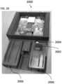
- FIG. 20 is a bottom-left perspective view of another example electrical connector housing 2000 in accordance with the teachings of the present disclosure.
- the connector housing 2000 includes a passthrough 2004 that connects a chamber for a circuit board to an outside of the connector housing 2000 .
- Frontend openings 2006 are also shown in the connector housing 2000 .
- Electrical leads for connecting a radio frequency identification (RFID) reader 2002 extend into the passthrough 2004 to connect the RFID reader 2002 to a circuit board within the connector housing 2000 .
- RFID reader 2002 is placed on an external portion of the connector housing 2000 that overlaps with another connector housing when two electrical connectors are mated. In this way, the RFID reader 2002 may read an RFID tag on another electrical connector. Therefore, the unique identifier read from another RFID tag may be identified.
- RFID radio frequency identification
- That unique identifier may be associated with the other electrical connector not shown, a battery charger to which the other electrical connector is connected, a battery to which the other electrical connector is connected, or any other device associated with the other electrical connector.
- a processor of the circuit board or another computing device with which the processor of the circuit board is in communication with may identify what device or connector the connector housing 2000 is connected to.
- the connector housing 2000 may have an RFID tag instead of the RFID reader 2002 or may have both an RFID tag and an RFID reader 2002 . By placing either an RFID tag or an RFID reader on the portion of the connector housing 2000 that overlaps with another connector, the RFID reader on one connector may overlap with the RFID tag on the other connector to read the tag.
- the RFID reader is shown mounted on a surface of the connector housing, an RFID reader or tag could also be formed within a portion of a connector housing in various embodiments.
- FIG. 21 is a block diagram view of an example system 2100 for an example electrical connector with a circuit board enclosed therein in accordance with the teachings of the present disclosure.
- the various aspects of the system 2100 may be mounted on a circuit board inside of a connector housing as disclosed herein, may be mounted on or in a connector housing and electrically connected to a circuit board inside of a connector housing, or may otherwise be in communication (e.g., wired or wireless) with components of a circuit board inside of a connector housing as disclosed herein.
- a processor 2102 and/or other devices of the system 2100 may be powered by a power source 2106 .
- the power source 2106 may be any type of power source, such as a battery or power pulled from current passing through an electrical contact within the electrical connector housing.
- the processor 2102 may be operatively coupled to a memory 2104 , an input button 2118 , one or more temperature sensor(s) 2110 , an RFID tag or reader 2112 , a display or light(s) 2114 , an input button 2118 (or other user interface), and a wireless transmitter 2116 .
- the memory 2104 may have stored thereon code (e.g., non-transient computer readable instructions) is stored and read or executed by the processor 706 .
- Such code may cause the processor 2102 to perform any of the actions, steps, methods, etc. disclosed herein.
- the memory 2104 may also store various sensor data captured, such as temperature, RFID tags read, voltage or current of signals read, etc., along with timestamps of any information sensed or determined by the components of the system 2100 .
- the processor 2102 may also communicate such data to another computing device 2200 through a wireless transmitter 2116 .
- the system 2100 and/or the computing device 2200 may further have any components of or may be the computing device described below with respect to FIG. 24 .
- the system 2100 may additionally communicate with the computing device 2200 or other computing devices through a wired connection.
- the temperature sensor(s) 2110 may be the temperature sensors disclosed herein that are used to monitor the temperature of various components within a connector housing, air within or outside the connector housing, or at a surface of a connector housing to monitor for a thermal runaway incident or any other temperature behavior or condition that is desirable to monitor for. As described below with respect to FIG. 23 , the processor may also transmit an alert to another computing device if a temperature sensed reaches or exceeds a predetermined threshold temperature that indicates a dangerous or undesirable temperature condition associated with an electrical connector housing, such as at a particular location on or in the housing or of a particular component within the housing.
- the wireless transmitter 2116 may communicate with the computing device 2200 .
- the computing device 2200 may be communicated with in various embodiments through a wired or wireless (e.g., Bluetooth) connection.
- the computing device 2200 may be any type of computing device, controller, processor, etc.
- the computing device 2200 may be smartphone, tablet, laptop, larger output display, specially built computing device for use with the system 2100 , a controller of a hydraulic or otherwise automated pipe bender, etc. In this way, the system 2100 may be configured to communicate with any other type of computing device.
- Data representative of the sensor measurements may be sent to the computing device 2200 via the wireless transmitter 2116 for display, collection, or any other purpose.
- the wireless transmitter 2116 may also be a transceiver that may receive signals/data from the computing device 2200 .
- An input button 2118 or other type of user input device may be incorporated into the system 2100 , so that a user may provide an input.
- the input button 2118 may be pressed to indicate to the system 2100 that data stored in the memory 2104 should be transmitted to the computing device 2200 .
- such transmission of data may occur automatically.
- a display/light(s) 2114 may provide feedback to a user.
- a green light emitting diode (LED) may indicate that the temperature of an electrical connector is acceptable, while a yellow or red LED may indicate that there is a problem with a connector or the temperature of the connector.
- additional, different, or fewer aspects than those shown in FIG. 21 may be used.
- additional sensors of the same type shown in FIG. 21 may be used, different types of sensors than those shown in FIG. 21 may be used, or fewer sensors than those shown in FIG. 21 may be used.
- Other devices or electronic components such as wireless radios, GPS chips, or any other type of electronic devices or components may be additionally or alternatively used.
- various electronic components may communicate with one another through wired or wireless connections, and may each communicate with a separate computing device (e.g., the computing device 2200 ) through wired or wireless connections in various embodiments.
- FIG. 22 is a flow chart illustrating an example method 2200 for assembling an electrical connector in accordance with the teachings of the present disclosure.
- a connector housing is formed, for example, out of a nonconductive plastic.
- one or more retainer springs may be inserted into one or more backend openings of the connector housing.
- retainer springs may be the retainer springs 1302 of FIGS. 13 , 15 , and 17 and the connector housing may be the connector housing 200 disclosed herein.
- the one or more retainer springs may be secured within the connector housing.
- Some retainer springs and connector housing may be shaped and configured to automatically retain and secure the retainer springs within the connector housing, while other types of retainer springs and connector housings may utilize a deformation of the connector housing (e.g., cold staking) to secure the retainer spring into the housing. In any case, the retainer springs are secured within the housing.
- a gasket e.g., the gasket 1402 of FIGS. 14 and 17
- a circuit board chamber e.g., the chamber 402 of FIGS. 4 , 11 B, 14 , and 16 - 19
- a circuit board e.g., the circuit board 1202 of FIGS. 12 - 14 , 17 , and 19
- the gasket and the circuit board may be inserted together after being adhered to one another or may be inserted separately.
- the circuit board may be secured within the connector housing.
- posts such as the posts 404 may be cold staked to form around and secure the circuit board.
- a circuit board chamber cover (e.g., the bottom cover 502 of FIGS. 5 , 11 A, 14 , 17 , and 19 ) may be placed and sealed over the circuit board chamber to protect the circuit board.
- a wire may be inserted into an electrical contact, and the electrical contact may be inserted into a backend opening of a connector housing at block 2218 .
- a frontend opening of the connector housing may be mated to a second connector housing as disclosed herein.
- the blocks 2216 , 2218 , and 2220 may be performed by a first user in the field using the electrical connector, while the other blocks may be performed by one or more other individuals at a manufacturing facility where the electrical connectors are manufactured.
- FIG. 23 is a flow chart illustrating an example method 2300 for determining a temperature at an electrical connector in accordance with the teachings of the present disclosure.
- a temperature sensor signal is received, for example, at a processor such as the processor 2102 of FIG. 21 . Based on that signal, the processor may determine the temperature at a temperature sensor associated with the temperature sensor signal and based on the temperature sensor signal.
- the temperature sensor signal itself may indicate the temperature to be determined, while in other embodiments the processor may have to perform additional processing on the temperature sensor signal to determine the temperature at the associated temperature sensor. Whether additional processing is used may depend, for example on the type of temperature sensor used.
- the determine temperature from the block 2304 may be compared to a predetermined temperature threshold to determine if a condition is unsafe and/or indicates conditions indicative of a potential thermal runaway event.
- the predetermined threshold temperature may be based on several different factors. For example, a placement of the temperature sensor may impact the predetermined threshold temperature. For example, a temperature may be measured at one or more of a surface of one of the electrical leads 1206 , a surface of one of the retainer springs 1302 , or at a surface of the electrical contact 1502 within a connector housing.
- temperatures may be hottest at electrical contact (e.g., the electrical contact 1502 ), for example, measurements of temperature at an electrical lead or retainer spring may be compared to a lower predetermined threshold temperature than a measurement of temperature at the electrical contact would be compared to.
- the predetermined temperature threshold may be configured based on a placement of a given temperature sensor.
- predetermined temperature thresholds may be configured based on a connector housing insulator type, connector amperage rating or other type or rating, connector housing thickness, connector housing material melting point, etc. In other words, the type of connector used and its intended use may indicate a capacity to withstand different temperatures, so the connector type and intended use may factor into setting a predetermined temperature threshold at which that connector may be safely used.
- a potential thermal runaway event may also be identified without using a predetermined temperature threshold or in addition to using a predetermined temperature threshold.
- temperature sensed in or on a connector housing (or of a particular component within the connector housing) may be monitored over time, and significant deviations from a typical temperature over time may indicate a potential thermal runaway event or misuse of the electrical connector.
- a processor may, for example, determine a running or overall average temperature at which a connector is operated, and monitor the temperature of the connector for deviations at or above a certain threshold percentage or other metric above the average temperature. In this way, even if a predetermined temperature threshold is not set or determined that might indicate dangerous temperatures for a connector, a processor may still monitor a connector temperature for deviations in temperature that may be unsafe and/or may cause the connector to fail.
- a temperature sensor may also be configured to measure an environment temperature (e.g., ambient air temperature) in which a connector is located.
- an ambient air temperature may be measured by a temperature sensor mounted on a circuit board or otherwise within a circuit board chamber (e.g., the chamber 402 disclosed herein). This may help determine what the predetermined threshold temperature used at the block 2306 should be, as hotter environments may make a connector more susceptible to thermal runaway events because heat may not dissipate as quickly from the connector itself. Accordingly, as described above, many different ways of determining that a temperature in or at a connector is unsafe may be utilized.
- an alert may be transmitted.
- the alert may be one or more of many different types of signals transmitted by a processor. For example, a signal may be sent to light on the connector to indicate that a condition is unsafe.
- An alert may be transmitted to another computing device through a wired or wireless connection. The other computing device may shut off power to the connector based on such an alert, for example, by shutting off a device the electrical connector is electrically connected to via a wire.
- a connector housing configuration for preventing thermal runaway events in an electrical connector. This can help identify instances of misuse of a connector (e.g., using a connector for a higher amperage than it is rated for), identify instances of mistakes made when using a connector (e.g., a bad crimp between and electrical contact and a wire), or identify when a device electrically connected with a connector is malfunctioning.
- Using the measurements of the connectors disclosed herein may also be used to prevent further damage (e.g., by shutting off a device associated with a connector in response to an alert or signal indicating a higher than desired temperature at a connector).
- voltage measured at an electrical contact may indicate a state or health of a battery to which the electrical contact is electrically connected to. Such a voltage measurement may also indicate a charge level of a battery. Similar to the alerts for temperature above, an alert may also be transmitted if a voltage meets or exceeds a first predetermined threshold or meets or is lower than a second predetermined threshold. In this way, if a voltage at a connector is undesirable or indicative of an undesirable condition elsewhere, an alert may be transmitted.
- FIG. 24 is a diagrammatic view of an example of a user computing environment that includes a general-purpose computing system environment 100 , such as a desktop computer, laptop, smartphone, tablet, or any other such device having the ability to execute instructions, such as those stored within a non-transient, computer-readable medium.
- a general-purpose computing system environment 100 such as a desktop computer, laptop, smartphone, tablet, or any other such device having the ability to execute instructions, such as those stored within a non-transient, computer-readable medium.
- Various computing devices as disclosed herein e.g., the angle indicator display devices, the computing devices
- computing system environment 100 typically includes at least one processing unit 102 and at least one memory 104 , which may be linked via a bus 106 .
- memory 104 may be volatile (such as RAM 110 ), non-volatile (such as ROM 108 , flash memory, etc.) or some combination of the two.
- Computing system environment 100 may have additional features and/or functionality.
- computing system environment 100 may also include additional storage (removable and/or non-removable) including, but not limited to, magnetic or optical disks, tape drives and/or flash drives.
- Such additional memory devices may be made accessible to the computing system environment 100 by means of, for example, a hard disk drive interface 112 , a magnetic disk drive interface 114 , and/or an optical disk drive interface 116 .
- these devices which would be linked to the system bus 306 , respectively, allow for reading from and writing to a hard disk 118 , reading from or writing to a removable magnetic disk 120 , and/or for reading from or writing to a removable optical disk 122 , such as a CD/DVD ROM or other optical media.
- the drive interfaces and their associated computer-readable media allow for the nonvolatile storage of computer readable instructions, data structures, program modules and other data for the computing system environment 100 .
- Computer readable media that can store data may be used for this same purpose.
- Examples of such media devices include, but are not limited to, magnetic cassettes, flash memory cards, digital videodisks, Bernoulli cartridges, random access memories, nano-drives, memory sticks, other read/write and/or read-only memories and/or any other method or technology for storage of information such as computer readable instructions, data structures, program modules or other data. Any such computer storage media may be part of computing system environment 100 .
- a number of program modules may be stored in one or more of the memory/media devices.
- a basic input/output system (BIOS) 124 containing the basic routines that help to transfer information between elements within the computing system environment 100 , such as during start-up, may be stored in ROM 108 .
- BIOS basic input/output system
- RAM 110 , hard drive 118 , and/or peripheral memory devices may be used to store computer executable instructions comprising an operating system 126 , one or more applications programs 128 (which may include the functionality disclosed herein, for example), other program modules 130 , and/or program data 122 .
- computer-executable instructions may be downloaded to the computing environment 100 as needed, for example, via a network connection.
- An end-user may enter commands and information into the computing system environment 100 through input devices such as a keyboard 134 and/or a pointing device 136 . While not illustrated, other input devices may include a microphone, a joystick, a game pad, a scanner, etc. These and other input devices would typically be connected to the processing unit 102 by means of a peripheral interface 138 which, in turn, would be coupled to bus 106 . Input devices may be directly or indirectly connected to processor 102 via interfaces such as, for example, a parallel port, game port, firewire, or a universal serial bus (USB). To view information from the computing system environment 100 , a monitor 140 or other type of display device may also be connected to bus 106 via an interface, such as via video adapter 132 . In addition to the monitor 140 , the computing system environment 100 may also include other peripheral output devices, not shown, such as speakers and printers.
- input devices such as a keyboard 134 and/or a pointing device 136 . While not illustrated, other input devices may include
- the computing system environment 100 may also utilize logical connections to one or more computing system environments. Communications between the computing system environment 100 and the remote computing system environment may be exchanged via a further processing device, such a network router 152 , that is responsible for network routing. Communications with the network router 152 may be performed via a network interface component 154 .
- a networked environment e.g., the Internet, World Wide Web, LAN, or other like type of wired or wireless network
- program modules depicted relative to the computing system environment 100 may be stored in the memory storage device(s) of the computing system environment 100 .
- the computing system environment 100 may also include localization hardware 186 for determining a location of the computing system environment 100 .
- the localization hardware 156 may include, for example only, a GPS antenna, an RFID chip or reader, a WiFi antenna, or other computing hardware that may be used to capture or transmit signals that may be used to determine the location of the computing system environment 100 .
- the data is represented as physical (electronic) quantities within the computer system's registers and memories and is transformed into other data similarly represented as physical quantities within the computer system memories or registers, or other such information storage, transmission, or display devices as described herein or otherwise understood to one of ordinary skill in the art.
Landscapes
- Engineering & Computer Science (AREA)
- Microelectronics & Electronic Packaging (AREA)
- Connector Housings Or Holding Contact Members (AREA)
- Details Of Connecting Devices For Male And Female Coupling (AREA)
- Coupling Device And Connection With Printed Circuit (AREA)
Abstract
Description
- The present description relates generally to electrical connectors, methods for assembling electrical connectors, and more particularly to an electrical connector housing that encloses a circuit board therein.
- In general, electrical connectors, including flat-wiping contact connectors, are known in the art. For example, flat-wiping contact technology may be used in applications such as electrical power connections for materials handling trucks, and single pole and dual pole flat wiping contact connectors may be used for storage battery connections.
- In one example, US Patent Application Publication No. 2009/0093149, incorporated herein by reference in its entirety, describes a flat-wiping contact and methods for producing them. For example, a plastic housing may be molded with a passageway or channel through the housing having a large backside opening intended for a conductor and a more defined front end opening for making the electrical connection to a mating connector. The passageway is configured with sidewall slots for locating and retaining a leaf spring that in turn retains the contact and provides the necessary wiping pressure for the contact when mated to another connector.
- A method for assembling such connectors may include inserting the spring into the housing through the large backside opening where it is locked into position in its slots by cold forming (staking) a portion of the plastic housing up behind the back end of the spring after the spring is inserted. External of the housing, a flat wiping contact is mated to a suitable conductor. The contact is then installed in the housing through the large back end opening, being slid forward until it latches over the front end of the spring.
- While the noted electrical connectors may be suitable for their intended purposes, there remains a strong desire for improved flat-wiping connectors that require easier assembly but still perform as a flat-wiping connector.
- Described herein are electrical connectors and methods for assembling electrical connectors that are configured to receive at least one electrical contact and enclose a circuit board within a connector housing of the electrical connectors. The electrical connectors further include at least one electrical lead configured to electrically connect the circuit board to the at least one electrical contact that may be inserted into the connector housing.
- A better appreciation of the objects, advantages, features, properties, and relationships of the subject matter disclosed herein will be obtained from the following detailed description and accompanying drawings which set forth illustrative examples which are indicative of the various ways in which the principles of the described embodiments may be employed.
-
FIG. 1A is a cross-sectional perspective view of an example electrical connector housing for a flat-wiping contact with a cold formed stake. -
FIG. 1B is a cross-sectional perspective view of the example electrical connector housing ofFIG. 1A with the flat-wiping contact installed. -
FIG. 2 is a top-right perspective view of an example electrical connector housing in accordance with the teachings of the present disclosure. -
FIG. 3 is a top-left perspective view of the electrical connector housing ofFIG. 2 in accordance with the teachings of the present disclosure. -
FIG. 4 is a bottom-front perspective view of the electrical connector housing ofFIG. 2 in accordance with the teachings of the present disclosure. -
FIG. 5 is a bottom-front perspective view of the electrical connector housing ofFIG. 2 with a bottom cover in accordance with the teachings of the present disclosure. -
FIG. 6 is a front elevational view of the electrical connector housing ofFIG. 2 in accordance with the teachings of the present disclosure. -
FIG. 7 is a rear elevational view of the electrical connector housing ofFIG. 2 in accordance with the teachings of the present disclosure. -
FIG. 8 is a right side elevational view of the electrical connector housing ofFIG. 2 in accordance with the teachings of the present disclosure. -
FIG. 9 is a left side elevational view of the electrical connector housing ofFIG. 2 in accordance with the teachings of the present disclosure. -
FIG. 10 is a top plan view of the electrical connector housing ofFIG. 2 in accordance with the teachings of the present disclosure. -
FIG. 11A is a bottom plan view of the electrical connector housing ofFIG. 2 with a bottom cover in accordance with the teachings of the present disclosure. -
FIG. 11B is a bottom plan view of the electrical connector housing ofFIG. 2 in accordance with the teachings of the present disclosure. -
FIG. 12 is a top-right perspective view of an example circuit board assembly in accordance with the teachings of the present disclosure. -
FIG. 13 is a front-right perspective view of the circuit board assembly ofFIG. 12 and two example retainer springs in accordance with the teachings of the present disclosure. -
FIG. 14 is an exploded perspective view of the electrical connector housing ofFIG. 2 , an example gasket, an example circuit board, and an example bottom cover in accordance with the teachings of the present disclosure. -
FIG. 15 is an exploded perspective view of the electrical connector housing ofFIG. 2 , a retainer spring, and an electrical contact in accordance with the teachings of the present disclosure. -
FIG. 16 is a cross-sectional front view of the electrical connector housing ofFIG. 2 taken along the cross-sectional line A shown inFIGS. 8 and 10 in accordance with the teachings of the present disclosure. -
FIG. 17 is a cross-sectional front view of an electrical connector assembly taken along the cross-sectional line A shown inFIGS. 8 and 10 in accordance with the teachings of the present disclosure. -
FIG. 18 is a cross-sectional front view of the electrical connector housing ofFIG. 2 taken along the cross-sectional line B shown inFIGS. 8 and 10 in accordance with the teachings of the present disclosure. -
FIG. 19 is a cross-sectional front view of an electrical connector assembly taken along the cross-sectional line B shown inFIGS. 8 and 10 in accordance with the teachings of the present disclosure. -
FIG. 20 is a bottom-left perspective view of another example electrical connector housing in accordance with the teachings of the present disclosure. -
FIG. 21 is a block diagram view of an example system for an example electrical connector with a circuit board enclosed therein in accordance with the teachings of the present disclosure. -
FIG. 22 is a flow chart illustrating an example method for assembling an electrical connector in accordance with the teachings of the present disclosure. -
FIG. 23 is a flow chart illustrating an example method for determining a temperature at an electrical connector in accordance with the teachings of the present disclosure. -
FIG. 24 is a diagrammatic view of an example of a user computing environment in accordance with the teachings of the present disclosure. - The following description of example methods and apparatus is not intended to limit the scope of the description to the precise form or forms detailed herein. Instead the following description is intended to be illustrative so that others may follow its teachings.
- Described herein are electrical connectors and methods for assembling electrical connectors that are configured to receive at least one electrical contact and enclose a circuit board within a connector housing of the electrical connectors. The electrical connectors further include at least one electrical lead configured to electrically connect the circuit board to the at least one electrical contact that may be inserted into the connector housing.
- Electrical connectors may be sized and rated differently for different uses. For example, the electrical contacts within a connector housing may be of varying sizes or may be made of varying materials depending on the intended use of the electrical contact. Similarly, a housing of an electrical connector, and may be shaped and sized based for specific uses and may be made out of varying insulating materials as desired. For example, some electrical connectors may be used to connect wiring of an electric vehicle to batteries to power the vehicle. Thus, the electrical connector may be designed based on the expected amperage (current) that will flow through the connector and a voltage of the system.
- As just one example, an electrical connector may be designed for 300 to 500 amps of current to flow through it. If the electrical connector is used for higher current flow than 500 amps, the electrical contact in the electrical connector may radiate excessive heat, which may in turn compromise the integrity of the electrical connector housing. This may be referred to as thermal runaway. For example, the electrical connector housing may warp, melt, etc. during a thermal runaway incident. In addition to using a connector for higher current flow than intended, thermal runaway may also occur if an electrical contact is not properly inserted into the housing, if the electrical contact is not properly contacting a second contact of a second connector, or if a wire is not properly crimped or otherwise affixed to an electrical contact. In any of these examples, failure of the electrical connector is possible. Even if the electrical connector does not completely fail, a malfunctioning electrical connector may have adverse effects on a load or power source that the electrical connector electrically connects together.
- Accordingly, disclosed herein are various electrical connector housing bodies and enclosed circuit boards that may be used to monitor for excessive heat indicative of a thermal runaway incident or measure other aspects of electricity flowing through an electrical connector to detect misuse of the electrical connector that may cause the electrical connector to fail or otherwise damage a load or power source connected by the electrical connector. A circuit board in an electrical connector may be used for other purposes as well, such as communicating with other computing devices via a wireless transceiver, a radio frequency identification (RFID) tag and/or reader, and/or any other type of wireless communication device.
- Referring to
FIGS. 1A and 1B , an example of a housing and a spring that does not have a circuit board enclosed therein is shown. In particular,FIGS. 1A and 1B illustrate a perspective view of asingle pole housing 10 for a flat wiping connector, sectioned to reveal the interior details. -
Backend opening 12 and front end opening 14 define a passageway, channel, or chamber throughhousing 10. The front end in this case is configured as a hermaphroditic or genderless connector, withcomplimentary chin 15 andU-shaped hood 17 structure able to be connected to another identical connector that is rotated 180 degrees, so that the contact surfaces engage properly. The opposing offset chins 15 align during connecting to enclose the engagedcontacts 32 and theU-shaped hoods 17 on each of the mating connectors act to longitudinally and rotationally align and accept the opposingconnector chin 15 in a straight-in connecting motion. The U-shaped hood restricts this type connector to only a straight-in connecting motion. - Referring again to
FIG. 1A ,leaf spring 16 is retained byspring base extensions 18 held in two opposing spring pockets or slots 20 (only one shown) proximate and parallel tofloor 24.Spring slots 20 are clearly configured to be open to or accessible from thebackend opening 12 for spring insertion. Theleaf spring 16 is inserted throughback end opening 12 so thatextensions 18 slide intoslots 20. The spring is retained in its final position inslots 20 byspring stake 26, driven upward by external pressure throughfloor 24, just aft of the base of the spring. Thestake 26 is cold formed into thefloor 24 of thehousing 10 after theleaf spring 16 is inserted into thehousing 10. Theleaf spring 16 is therefore locked into position because the front edges of theextensions 18 are limited from moving past a front edge of theslots 20, and the rear edge of theleaf spring 16 is limited from moving by thestake 26. Theleaf spring 16's cantilevered forward end extends past thebarrier wall 22 and is biased upwards away fromfloor 24. - Referring to
FIG. 1B for the description of assembly;contact 30 comprises a frontend wiping surface 32, terminated byspring hook 34, and a backend conductor receiver 36. (The conductor is not shown.)Contact 30 is installed by being inserted intobackend opening 12 so that the frontend wiping surface 32 passed underbarrier wall 22, riding along on upwardly biasedleaf spring 16 untilspring hook 34 latches or snaps over the forward edge or end of theleaf spring 16. The housing is dimensionally configured so that the forward end ofconductor receiver 36 abutsbarrier wall 22 at this point, wherebycontact 30 is locked in its position, restrained from further forward or aft motion and limited to only vertical motion by compression ofleaf spring 16. - Thereafter in operation, floating action provided by
spring 16 enablescontact 30 to be depressed sufficiently during mating with another opposing connector to accept the slight vertical displacement caused by the wiping motion that brings the two opposing contacts into a compressive engagement of their respective wiping surfaces 32 through which electrical current is passed. - However, as discussed above, misuse of electrical connectors or damage to electrical connectors can cause the connectors to fail and/or cause damage to whatever the electrical connectors are electrically joining together. The connectors shown in and described with respect to
FIGS. 1A and 1B have no mechanism for measuring or determining when conditions for failure or potential damage to other devices are present. Accordingly, disclosed herein are various connector housings that are configured to enclose a circuit board, and may have other components in the electrical connector for monitoring the state of the connector (e.g., temperature, voltage, current, etc.). Additionally, methods for assembling such connectors are disclosed herein. -
FIG. 2 is a top-right perspective view of an exampleelectrical connector housing 200 in accordance with the teachings of the present disclosure. Theconnector housing 200 includesbackend opening 202 into which an electrical contact (not shown inFIG. 2 ) may be inserted. Theexample connector housing 200 is a flat-wiping connector, but the various systems and methods described herein may be used with other types of connectors than flat-wiping connectors. -
FIG. 3 is a top-left perspective view of theelectrical connector housing 200 ofFIG. 2 in accordance with the teachings of the present disclosure. InFIG. 3 ,frontend openings 302 are shown, which are configured to mate with another connector, so that a load may be connected to a power source, for example. Theconnector housing 200 also includesholes 304. Theholes 304 are configured to receive pins that are directly connected to a circuit board enclosed within theconnector housing 200. In this way, the pins extending out of theholes 304 may serve as a male connector for joining the circuit board within theconnector housing 200 to circuitry of an opposing connector mated to theconnector housing 200. In another embodiment, theholes 304 may receive pins that are a part of a connector mated to theconnector housing 200. In this way, theholes 304 may serve as a female side connector for the electrically joining the circuit board within theconnector housing 200 to circuitry in an opposing connector. In any case, theholes 304 may accommodate electrical connection to a circuit board within the connector housing. -
FIG. 4 is a bottom-front perspective view of theelectrical connector housing 200 ofFIG. 2 in accordance with the teachings of the present disclosure. The view of theconnector housing 200 shows achamber 402 in the bottom of theconnector housing 200 in which a circuit board may be mounted or otherwise placed. Such a circuit board is not shown inFIG. 4 but is shown in and discussed further with respect toFIGS. 12-14, 17, and 19 . Further shown inFIG. 4 areposts 404 molded into theconnector housing 200 that may be used for mounting a circuit board to theconnector housing 200. In various embodiments, a circuit board may be affixed to or secured into theconnector housing 200 using methods or components other than theposts 404 or in addition to theposts 404. - The
connector housing 200 also includespassthroughs 406 for electrical leads to pass from thechamber 402 into a second chamber or passageway of theconnector housing 200. In this way, an electrical lead may connect a circuit board in thechamber 402 to electrically conductive components, sensors, etc. other portions of chambers of theconnector housing 200. In addition, apassthrough 408 provides an opening for electrical leads or pins to connect a circuit board within thechamber 402 to theholes 304 ofFIG. 3 so that the circuit board may electrically connect to something outside of theconnector housing 200. In various embodiments, additional, different, or fewer passthroughs than thepassthroughs connector housing 200 may also be sealed after electrical components are inserted therethrough to separate or seal a chamber for a circuit board and other chamber(s) of the electrical connector. -
FIG. 5 is a bottom-front perspective view of the electrical connector housing 500 ofFIG. 2 with a bottom cover in accordance with the teachings of the present disclosure. The connector housing 500 shown inFIG. 5 includes abottom cover 502 placed over thechamber 402 shown inFIG. 4 . Thebottom cover 502 may be affixed, sealed, or otherwise connected to theconnector housing 200 to protect the circuit board and any other components in thechamber 402. -
FIG. 6 is a front elevational view of theelectrical connector housing 200 ofFIG. 2 in accordance with the teachings of the present disclosure.FIG. 7 is a rear elevational view of theelectrical connector housing 200 ofFIG. 2 in accordance with the teachings of the present disclosure. -
FIG. 8 is a right side elevational view of theelectrical connector housing 200 ofFIG. 2 in accordance with the teachings of the present disclosure.FIG. 9 is a left side elevational view of theelectrical connector housing 200 ofFIG. 2 in accordance with the teachings of the present disclosure. Theconnector housing 200 as shown inFIG. 8 includes apin cover 802 that may cover and protect pins that are running from a circuit board in theconnector housing 200 to theholes 304 of theconnector housing 200. In some embodiments, thepin cover 802 may not be present in theconnector housing 200 itself, but may be mounted on or otherwise be a part of a circuit board in theconnector housing 200. In addition,FIG. 8 shows cross-sectional lines A and B. Cross-sectional views of theconnector housing 200 associated with the cross-sectional lines A and B are shown inFIGS. 16 and 18 , respectively.FIG. 10 is a top plan view of theelectrical connector housing 200 ofFIG. 2 in accordance with the teachings of the present disclosure.FIG. 10 also shows the cross-sectional lines A and B that are depicted inFIGS. 16 and 18 , respectively. -
FIG. 11A is a bottom plan view of theelectrical connector housing 200 ofFIG. 2 with thebottom cover 502 in accordance with the teachings of the present disclosure.FIG. 11B is a bottom plan view of theelectrical connector housing 200 without thebottom cover 502 ofFIG. 2 in accordance with the teachings of the present disclosure. Also shown inFIG. 11A arepins 1102 that may pass through theholes 304 as described herein, which are not shown inFIG. 11B . LikeFIG. 4 ,FIG. 11B without thebottom cover 502 shows thechamber 402 configured to house a circuit board, theposts 404 for mounting a circuit board, thepassthroughs 406 for connecting a circuit board to components inside other passageways or chambers of theconnector housing 200, and thepassthrough 408 for pins to connect a circuit board to another device or connector. -
FIG. 12 is a top-right perspective view of an examplecircuit board assembly 1200 in accordance with the teachings of the present disclosure.FIG. 13 is a front-right perspective view of thecircuit board assembly 1200 ofFIG. 12 and twoexample retainer springs 1302 in accordance with the teachings of the present disclosure. The components of thecircuit board assembly 1200 may be assembled and connected before insertion into an electrical connector housing such as theconnector housing 200 disclosed herein. Thecircuit board assembly 1200 includes a circuit board 1202 (circuitry not shown), and thecircuit board 1202 hasholes 1204 to accommodate theposts 404 shown inFIGS. 4 and 11B . Theholes 1204 may fit over theposts 404, and thecircuit board 1202 may fit to theposts 404 in various ways. For example, theposts 404 may be heat staked to slightly melt around and secure thecircuit board 1202 within thechamber 402. In other examples, adhesive may be used to attach thecircuit board 1202 to theposts 404, an interference fit between thecircuit board 1202 and theposts 404 may be used to attach thecircuit board 1202 to theposts 404, or any other suitable method of securing thecircuit board 1202 within a chamber of the connector housing may be used in various embodiments. - The
circuit board assembly 1200 further includeselectrical leads 1206 attached to the circuit board. The electrical leads 1206 may be shaped such that, when they are in contact with the retainer springs 1302, theelectrical leads 1206 have a spring force that pushes back on the retainer springs 1302 to maintain an electrical connection between the retainer springs 1302 and thecircuit board 1204. In addition, theelectrical leads 1206 are shaped such that during insertion of the retainer springs 1302 into a connector housing such as theconnector housing 200 will slide along theelectrical leads 1206 without catching on the electrical leads 1206.FIGS. 12 and 13 demonstrate just one possible way of electrically connecting thecircuit board 1202 to the retainer springs 1302, but any other ways of connecting the two may be used in various embodiments. In addition, though the embodiments ofFIG. 13 relates to connecting thecircuit board 1202 to the retainer springs 1302, similar or different electrical leads may electrically connect thecircuit board 1202 directly or indirectly to other components within a connector body, such as an electrical contact, a sensor, or any other component. The circuit board assembly further includes thepin cover 802 that coverspins 1210 that electrically connect thecircuit board 1202 to a device or connector external to the connector in which thecircuit board 1202 is enclosed. -
FIG. 14 is an exploded perspective view of theelectrical connector housing 200 ofFIG. 2 , anexample gasket 1402, thecircuit board 1202, and thebottom cover 502 in accordance with the teachings of the present disclosure. In particular,FIG. 14 shows how thegasket 1402 may be placed between thecircuit board 1202 and a surface of thechamber 402 into which thecircuit board 1202 is mounted. Thegasket 1402 may include holes to accommodate theposts 404 that are used to mountcircuit board 1202, as well as openings that align with thepassthroughs circuit board 1202 to devices, sensors, components, etc. within theconnector housing 200. Thegasket 1402 further serves to seal thecircuit board 1202 and components thereof from the rest of theconnector housing 200, including around thepassthroughs -
FIG. 15 is an exploded perspective view of theelectrical connector housing 200 ofFIG. 2 , theretainer spring 1302, and anelectrical contact 1502 in accordance with the teachings of the present disclosure. When using theelectrical connector 202, theretainer spring 1302 is first inserted into thebackend opening 202. Theretainer spring 1302 is secured into theconnector housing 200 after insertion. A wire may be inserted into an opening of theelectrical contact 1502 and the electrical contact is crimped around the wire. Theelectrical contact 1502 may then be inserted into thebackend opening 202, and upon full insertion, theelectrical contact 1502 is retained within theconnector housing 200 by theretainer spring 1302. -
FIG. 16 is a cross-sectional front view of theelectrical connector housing 200 ofFIG. 2 taken along the cross-sectional line A shown inFIGS. 8 and 10 in accordance with the teachings of the present disclosure. The example ofFIG. 16 shows theconnector housing 200 without a circuit board, gasket, bottom cover, retainer spring, or electrical contact installed therein. Theconnector housing 200 includes thebackend opening 202 through which a retainer spring and an electrical contact may be inserted as disclosed herein. Theconnector housing 200 further includes thefrontend opening 302, which may mate with another connector housing similar to theconnector housing 200 as disclosed herein, in order to cause an electrical contact in the two connector housings to also mate.FIG. 16 further shows thechamber 402 in which a circuit board may be mounted and achamber 1602 in which an electrical contact may be inserted. The passthrough 406 (as well as thepassthrough 408 and anotherpassthrough 406, which are not shown inFIG. 16 ) connects thechamber 402 and thechamber 1602, so that electrical leads (e.g., the electrical leads 1206) or other components may extend from a circuit board in thechamber 402 into thechamber 1602.FIG. 16 further shows theposts 404 which may be used to mount or secure a circuit board within thechamber 402. -
FIG. 17 is a cross-sectional front view of an electrical connector assembly taken along the cross-sectional line A shown inFIGS. 8 and 10 in accordance with the teachings of the present disclosure. In particular,FIG. 17 shows an assembly with theretainer spring 1302, theelectrical contact 1502, thegasket 1402, thecircuit board 1202, theelectrical lead 1206, and thebottom cover 502 all in place. As shown inFIG. 17 , theelectrical lead 1206 may extend from thecircuit board 1202 to theretainer spring 1302. Theelectrical lead 1206, theretainer spring 1302, and theelectrical contact 1502 may all be formed from electrically conductive material, such as an electrically conductive metal. In this way, components on thecircuit board 1202 may be able to detect aspects of electricity or electrical signals in theelectrical contact 1502 and a wire within theelectrical contact 1502. For example, a voltage of theelectrical contact 1502 and theretainer spring 1302 may be sensed. In the embodiment ofFIG. 17 , only a singleelectrical lead 1206 contacts theretainer spring 1302. However, in other embodiments, a connector housing may be configured to provide multiple passthroughs such that multiple electrical leads may be in contact with a retainer spring and/or electrical contact. In this way, other aspects of signals passing through theelectrical contact 1502 may be measured, such as current passing through theelectrical contact 1502. -
FIG. 18 is a cross-sectional front view of theelectrical connector housing 200 ofFIG. 2 taken along the cross-sectional line B shown inFIGS. 8 and 10 in accordance with the teachings of the present disclosure.FIG. 18 specifically shows the passthrough 408 that connects thechamber 402 for a circuit board to achamber 1802. Thechamber 1802 is separate from thechamber 1602, to isolate an electrical contact in thechamber 1602 from thechamber 1802 and another chamber in which a second electrical contact is inserted. Theholes 304 provide an opening for pins to pass from inside the connector housing 200 (e.g., the chamber 1802) to outside of theconnector housing 200. -
FIG. 19 is a cross-sectional front view of an electrical connector assembly taken along the cross-sectional line B shown inFIGS. 8 and 10 in accordance with the teachings of the present disclosure.FIG. 19 shows how thepins 1210 may pass from thecircuit board 1202, through the passthrough 408 to thechamber 1802, and through theholes 304 to an outside of theconnector housing 200. In this way, thepins 1210 may, for example, contact another electrical connector to facilitate communication between two electrical connectors. Thepins 1210 may be protected in part or in whole within thechamber 1802 by thepin cover 802, which may also extend from thecircuit board 1202 through the passthrough 408, and into thechamber 1802. - In various embodiments, the
circuit board 1202 may include or may be connected to various components for measuring conditions of an electrical connector, contacts within the electrical connector, air/environment within or outside the electrical connector, or any other aspect of the electrical connector or related to the electrical connector. For example, a temperature sensor may be located on thecircuit board 1202 or anywhere within theconnector housing 200. For example, a temperature sensor may be located within thechamber 402, within thechamber 1602, within thechamber 1802, or anywhere on an external surface of theconnector housing 200. Additionally or alternatively, temperature sensors may be located to be in contact with one or more of theelectrical leads 1206, theretainer spring 1302, theelectrical contact 1502, thepins 1210, and/or any other component within theconnector housing 200. In various embodiments, other types of sensors may also be incorporated into any location within or on theconnector housing 200 or on components within theconnector housing 200. For example, moisture or humidity sensors or any other type of sensors may be used to monitor a condition of and/or environment of a connector housing. Any various sensors incorporated into theconnector housing 200 may also include electrical leads that run from a sensor to thecircuit board 1202 so that measurements from those sensors may be detected/received. Electrical leads may run from said sensors through one of thepassthroughs -
FIG. 20 is a bottom-left perspective view of another exampleelectrical connector housing 2000 in accordance with the teachings of the present disclosure. Theconnector housing 2000 includes a passthrough 2004 that connects a chamber for a circuit board to an outside of theconnector housing 2000.Frontend openings 2006 are also shown in theconnector housing 2000. Electrical leads for connecting a radio frequency identification (RFID)reader 2002 extend into the passthrough 2004 to connect theRFID reader 2002 to a circuit board within theconnector housing 2000. TheRFID reader 2002 is placed on an external portion of theconnector housing 2000 that overlaps with another connector housing when two electrical connectors are mated. In this way, theRFID reader 2002 may read an RFID tag on another electrical connector. Therefore, the unique identifier read from another RFID tag may be identified. That unique identifier may be associated with the other electrical connector not shown, a battery charger to which the other electrical connector is connected, a battery to which the other electrical connector is connected, or any other device associated with the other electrical connector. In this way, a processor of the circuit board or another computing device with which the processor of the circuit board is in communication with may identify what device or connector theconnector housing 2000 is connected to. In another embodiment, theconnector housing 2000 may have an RFID tag instead of theRFID reader 2002 or may have both an RFID tag and anRFID reader 2002. By placing either an RFID tag or an RFID reader on the portion of theconnector housing 2000 that overlaps with another connector, the RFID reader on one connector may overlap with the RFID tag on the other connector to read the tag. Although the RFID reader is shown mounted on a surface of the connector housing, an RFID reader or tag could also be formed within a portion of a connector housing in various embodiments. -
FIG. 21 is a block diagram view of anexample system 2100 for an example electrical connector with a circuit board enclosed therein in accordance with the teachings of the present disclosure. The various aspects of thesystem 2100 may be mounted on a circuit board inside of a connector housing as disclosed herein, may be mounted on or in a connector housing and electrically connected to a circuit board inside of a connector housing, or may otherwise be in communication (e.g., wired or wireless) with components of a circuit board inside of a connector housing as disclosed herein. - In particular, a
processor 2102 and/or other devices of thesystem 2100 may be powered by apower source 2106. Thepower source 2106 may be any type of power source, such as a battery or power pulled from current passing through an electrical contact within the electrical connector housing. Theprocessor 2102 may be operatively coupled to amemory 2104, aninput button 2118, one or more temperature sensor(s) 2110, an RFID tag or reader 2112, a display or light(s) 2114, an input button 2118 (or other user interface), and awireless transmitter 2116. Thememory 2104 may have stored thereon code (e.g., non-transient computer readable instructions) is stored and read or executed by the processor 706. Such code may cause theprocessor 2102 to perform any of the actions, steps, methods, etc. disclosed herein. Thememory 2104 may also store various sensor data captured, such as temperature, RFID tags read, voltage or current of signals read, etc., along with timestamps of any information sensed or determined by the components of thesystem 2100. Theprocessor 2102 may also communicate such data to anothercomputing device 2200 through awireless transmitter 2116. Thesystem 2100 and/or thecomputing device 2200 may further have any components of or may be the computing device described below with respect toFIG. 24 . In various embodiments, thesystem 2100 may additionally communicate with thecomputing device 2200 or other computing devices through a wired connection. - The temperature sensor(s) 2110 may be the temperature sensors disclosed herein that are used to monitor the temperature of various components within a connector housing, air within or outside the connector housing, or at a surface of a connector housing to monitor for a thermal runaway incident or any other temperature behavior or condition that is desirable to monitor for. As described below with respect to
FIG. 23 , the processor may also transmit an alert to another computing device if a temperature sensed reaches or exceeds a predetermined threshold temperature that indicates a dangerous or undesirable temperature condition associated with an electrical connector housing, such as at a particular location on or in the housing or of a particular component within the housing. - The
wireless transmitter 2116 may communicate with thecomputing device 2200. Thecomputing device 2200 may be communicated with in various embodiments through a wired or wireless (e.g., Bluetooth) connection. Thecomputing device 2200 may be any type of computing device, controller, processor, etc. For example, thecomputing device 2200 may be smartphone, tablet, laptop, larger output display, specially built computing device for use with thesystem 2100, a controller of a hydraulic or otherwise automated pipe bender, etc. In this way, thesystem 2100 may be configured to communicate with any other type of computing device. - Data representative of the sensor measurements (e.g., the temperature sensor(s) 2110, the RFID reader 2112, the signal sensor(s) 2108) may be sent to the
computing device 2200 via thewireless transmitter 2116 for display, collection, or any other purpose. In various examples, thewireless transmitter 2116 may also be a transceiver that may receive signals/data from thecomputing device 2200. - An
input button 2118 or other type of user input device may be incorporated into thesystem 2100, so that a user may provide an input. For example, theinput button 2118 may be pressed to indicate to thesystem 2100 that data stored in thememory 2104 should be transmitted to thecomputing device 2200. In other embodiments, such transmission of data may occur automatically. A display/light(s) 2114 may provide feedback to a user. For example, a green light emitting diode (LED) may indicate that the temperature of an electrical connector is acceptable, while a yellow or red LED may indicate that there is a problem with a connector or the temperature of the connector. - In various embodiments, additional, different, or fewer aspects than those shown in
FIG. 21 may be used. For example, additional sensors of the same type shown inFIG. 21 may be used, different types of sensors than those shown inFIG. 21 may be used, or fewer sensors than those shown inFIG. 21 may be used. Other devices or electronic components such as wireless radios, GPS chips, or any other type of electronic devices or components may be additionally or alternatively used. In addition, as disclosed herein, various electronic components (whether shown inFIG. 21 or not) may communicate with one another through wired or wireless connections, and may each communicate with a separate computing device (e.g., the computing device 2200) through wired or wireless connections in various embodiments. -
FIG. 22 is a flow chart illustrating anexample method 2200 for assembling an electrical connector in accordance with the teachings of the present disclosure. Atblock 2202, a connector housing is formed, for example, out of a nonconductive plastic. Atblock 2204, one or more retainer springs may be inserted into one or more backend openings of the connector housing. For example, retainer springs may be the retainer springs 1302 ofFIGS. 13, 15, and 17 and the connector housing may be theconnector housing 200 disclosed herein. - At
block 2206, the one or more retainer springs may be secured within the connector housing. Some retainer springs and connector housing may be shaped and configured to automatically retain and secure the retainer springs within the connector housing, while other types of retainer springs and connector housings may utilize a deformation of the connector housing (e.g., cold staking) to secure the retainer spring into the housing. In any case, the retainer springs are secured within the housing. - At
block 2208, a gasket (e.g., thegasket 1402 ofFIGS. 14 and 17 ) is inserted into a circuit board chamber (e.g., thechamber 402 ofFIGS. 4, 11B, 14, and 16-19 ). Atblock 2210, a circuit board (e.g., thecircuit board 1202 ofFIGS. 12-14, 17, and 19 ) is inserted into the circuit board chamber. In various embodiments, the gasket and the circuit board may be inserted together after being adhered to one another or may be inserted separately. Atblock 2212, the circuit board may be secured within the connector housing. For example, as disclosed herein, posts such as theposts 404 may be cold staked to form around and secure the circuit board. - At
block 2214, a circuit board chamber cover (e.g., thebottom cover 502 ofFIGS. 5, 11A, 14, 17, and 19 ) may be placed and sealed over the circuit board chamber to protect the circuit board. - At
block 2216, a wire may be inserted into an electrical contact, and the electrical contact may be inserted into a backend opening of a connector housing atblock 2218. Atblock 2220, a frontend opening of the connector housing may be mated to a second connector housing as disclosed herein. In various embodiments, theblocks -
FIG. 23 is a flow chart illustrating anexample method 2300 for determining a temperature at an electrical connector in accordance with the teachings of the present disclosure. Atblock 2302, a temperature sensor signal is received, for example, at a processor such as theprocessor 2102 ofFIG. 21 . Based on that signal, the processor may determine the temperature at a temperature sensor associated with the temperature sensor signal and based on the temperature sensor signal. In some embodiments, the temperature sensor signal itself may indicate the temperature to be determined, while in other embodiments the processor may have to perform additional processing on the temperature sensor signal to determine the temperature at the associated temperature sensor. Whether additional processing is used may depend, for example on the type of temperature sensor used. - At
block 2306, the determine temperature from theblock 2304 may be compared to a predetermined temperature threshold to determine if a condition is unsafe and/or indicates conditions indicative of a potential thermal runaway event. The predetermined threshold temperature may be based on several different factors. For example, a placement of the temperature sensor may impact the predetermined threshold temperature. For example, a temperature may be measured at one or more of a surface of one of theelectrical leads 1206, a surface of one of the retainer springs 1302, or at a surface of theelectrical contact 1502 within a connector housing. Because temperatures may be hottest at electrical contact (e.g., the electrical contact 1502), for example, measurements of temperature at an electrical lead or retainer spring may be compared to a lower predetermined threshold temperature than a measurement of temperature at the electrical contact would be compared to. Similarly, different locations within a connector housing or on surfaces outside or inside a connector housing may have different expected temperatures based on where a source of heat is that is indicative of a potential thermal runaway even. Thus, the predetermined temperature threshold may be configured based on a placement of a given temperature sensor. In addition, predetermined temperature thresholds may be configured based on a connector housing insulator type, connector amperage rating or other type or rating, connector housing thickness, connector housing material melting point, etc. In other words, the type of connector used and its intended use may indicate a capacity to withstand different temperatures, so the connector type and intended use may factor into setting a predetermined temperature threshold at which that connector may be safely used. - In various embodiments, a potential thermal runaway event may also be identified without using a predetermined temperature threshold or in addition to using a predetermined temperature threshold. For example, temperature sensed in or on a connector housing (or of a particular component within the connector housing) may be monitored over time, and significant deviations from a typical temperature over time may indicate a potential thermal runaway event or misuse of the electrical connector. In other words, a processor may, for example, determine a running or overall average temperature at which a connector is operated, and monitor the temperature of the connector for deviations at or above a certain threshold percentage or other metric above the average temperature. In this way, even if a predetermined temperature threshold is not set or determined that might indicate dangerous temperatures for a connector, a processor may still monitor a connector temperature for deviations in temperature that may be unsafe and/or may cause the connector to fail.
- In various embodiments, a temperature sensor may also be configured to measure an environment temperature (e.g., ambient air temperature) in which a connector is located. For example, an ambient air temperature may be measured by a temperature sensor mounted on a circuit board or otherwise within a circuit board chamber (e.g., the
chamber 402 disclosed herein). This may help determine what the predetermined threshold temperature used at theblock 2306 should be, as hotter environments may make a connector more susceptible to thermal runaway events because heat may not dissipate as quickly from the connector itself. Accordingly, as described above, many different ways of determining that a temperature in or at a connector is unsafe may be utilized. - At
block 2308, if it is determined that a temperature in a connector is above a predetermined temperature threshold (or if it is otherwise determined that the connector has reached a potentially unsafe temperature), an alert may be transmitted. The alert may be one or more of many different types of signals transmitted by a processor. For example, a signal may be sent to light on the connector to indicate that a condition is unsafe. An alert may be transmitted to another computing device through a wired or wireless connection. The other computing device may shut off power to the connector based on such an alert, for example, by shutting off a device the electrical connector is electrically connected to via a wire. - Accordingly, disclosed herein are various sensors and connector housing configurations for preventing thermal runaway events in an electrical connector. This can help identify instances of misuse of a connector (e.g., using a connector for a higher amperage than it is rated for), identify instances of mistakes made when using a connector (e.g., a bad crimp between and electrical contact and a wire), or identify when a device electrically connected with a connector is malfunctioning. Using the measurements of the connectors disclosed herein may also be used to prevent further damage (e.g., by shutting off a device associated with a connector in response to an alert or signal indicating a higher than desired temperature at a connector).
- In addition, other aspects sensed at an electrical connector as disclosed herein may be useful in other ways. For example, voltage measured at an electrical contact may indicate a state or health of a battery to which the electrical contact is electrically connected to. Such a voltage measurement may also indicate a charge level of a battery. Similar to the alerts for temperature above, an alert may also be transmitted if a voltage meets or exceeds a first predetermined threshold or meets or is lower than a second predetermined threshold. In this way, if a voltage at a connector is undesirable or indicative of an undesirable condition elsewhere, an alert may be transmitted.
-
FIG. 24 is a diagrammatic view of an example of a user computing environment that includes a general-purposecomputing system environment 100, such as a desktop computer, laptop, smartphone, tablet, or any other such device having the ability to execute instructions, such as those stored within a non-transient, computer-readable medium. Various computing devices as disclosed herein (e.g., the angle indicator display devices, the computing devices) may be similar to thecomputing system 100 or may include some components of thecomputing system 100. Furthermore, while described and illustrated in the context of asingle computing system 100, those skilled in the art will also appreciate that the various tasks described hereinafter may be practiced in a distributed environment havingmultiple computing systems 100 linked via a local or wide-area network in which the executable instructions may be associated with and/or executed by one or more ofmultiple computing systems 100. - In its most basic configuration,
computing system environment 100 typically includes at least one processing unit 102 and at least onememory 104, which may be linked via abus 106. Depending on the exact configuration and type of computing system environment,memory 104 may be volatile (such as RAM 110), non-volatile (such as ROM 108, flash memory, etc.) or some combination of the two.Computing system environment 100 may have additional features and/or functionality. For example,computing system environment 100 may also include additional storage (removable and/or non-removable) including, but not limited to, magnetic or optical disks, tape drives and/or flash drives. Such additional memory devices may be made accessible to thecomputing system environment 100 by means of, for example, a harddisk drive interface 112, a magneticdisk drive interface 114, and/or an opticaldisk drive interface 116. As will be understood, these devices, which would be linked to the system bus 306, respectively, allow for reading from and writing to ahard disk 118, reading from or writing to a removablemagnetic disk 120, and/or for reading from or writing to a removableoptical disk 122, such as a CD/DVD ROM or other optical media. The drive interfaces and their associated computer-readable media allow for the nonvolatile storage of computer readable instructions, data structures, program modules and other data for thecomputing system environment 100. Those skilled in the art will further appreciate that other types of computer readable media that can store data may be used for this same purpose. Examples of such media devices include, but are not limited to, magnetic cassettes, flash memory cards, digital videodisks, Bernoulli cartridges, random access memories, nano-drives, memory sticks, other read/write and/or read-only memories and/or any other method or technology for storage of information such as computer readable instructions, data structures, program modules or other data. Any such computer storage media may be part ofcomputing system environment 100. - A number of program modules may be stored in one or more of the memory/media devices. For example, a basic input/output system (BIOS) 124, containing the basic routines that help to transfer information between elements within the
computing system environment 100, such as during start-up, may be stored in ROM 108. Similarly,RAM 110,hard drive 118, and/or peripheral memory devices may be used to store computer executable instructions comprising anoperating system 126, one or more applications programs 128 (which may include the functionality disclosed herein, for example),other program modules 130, and/orprogram data 122. Still further, computer-executable instructions may be downloaded to thecomputing environment 100 as needed, for example, via a network connection. - An end-user may enter commands and information into the
computing system environment 100 through input devices such as akeyboard 134 and/or apointing device 136. While not illustrated, other input devices may include a microphone, a joystick, a game pad, a scanner, etc. These and other input devices would typically be connected to the processing unit 102 by means of aperipheral interface 138 which, in turn, would be coupled tobus 106. Input devices may be directly or indirectly connected to processor 102 via interfaces such as, for example, a parallel port, game port, firewire, or a universal serial bus (USB). To view information from thecomputing system environment 100, amonitor 140 or other type of display device may also be connected tobus 106 via an interface, such as viavideo adapter 132. In addition to themonitor 140, thecomputing system environment 100 may also include other peripheral output devices, not shown, such as speakers and printers. - The
computing system environment 100 may also utilize logical connections to one or more computing system environments. Communications between thecomputing system environment 100 and the remote computing system environment may be exchanged via a further processing device, such anetwork router 152, that is responsible for network routing. Communications with thenetwork router 152 may be performed via anetwork interface component 154. Thus, within such a networked environment, e.g., the Internet, World Wide Web, LAN, or other like type of wired or wireless network, it will be appreciated that program modules depicted relative to thecomputing system environment 100, or portions thereof, may be stored in the memory storage device(s) of thecomputing system environment 100. - The
computing system environment 100 may also include localization hardware 186 for determining a location of thecomputing system environment 100. In some instances, thelocalization hardware 156 may include, for example only, a GPS antenna, an RFID chip or reader, a WiFi antenna, or other computing hardware that may be used to capture or transmit signals that may be used to determine the location of thecomputing system environment 100. - While this disclosure has described certain embodiments, it will be understood that the claims are not intended to be limited to these embodiments except as explicitly recited in the claims. On the contrary, the instant disclosure is intended to cover alternatives, modifications and equivalents, which may be included within the spirit and scope of the disclosure. Furthermore, in the detailed description of the present disclosure, numerous specific details are set forth in order to provide a thorough understanding of the disclosed embodiments. However, it will be obvious to one of ordinary skill in the art that systems and methods consistent with this disclosure may be practiced without these specific details. In other instances, well known methods, procedures, components, and circuits have not been described in detail as not to unnecessarily obscure various aspects of the present disclosure.
- Some portions of the detailed descriptions of this disclosure have been presented in terms of procedures, logic blocks, processing, and other symbolic representations of operations on data bits within a computer or digital system memory. These descriptions and representations are the means used by those skilled in the data processing arts to most effectively convey the substance of their work to others skilled in the art. A procedure, logic block, process, etc., is herein, and generally, conceived to be a self-consistent sequence of steps or instructions leading to a desired result. The steps are those requiring physical manipulations of physical quantities. Usually, though not necessarily, these physical manipulations take the form of electrical or magnetic data capable of being stored, transferred, combined, compared, and otherwise manipulated in a computer system or similar electronic computing device. For reasons of convenience, and with reference to common usage, such data is referred to as bits, values, elements, symbols, characters, terms, numbers, or the like, with reference to various presently disclosed embodiments.
- It should be borne in mind, however, that these terms are to be interpreted as referencing physical manipulations and quantities and are merely convenient labels that should be interpreted further in view of terms commonly used in the art. Unless specifically stated otherwise, as apparent from the discussion herein, it is understood that throughout discussions of the present embodiment, discussions utilizing terms such as “determining” or “outputting” or “transmitting” or “recording” or “locating” or “storing” or “displaying” or “receiving” or “recognizing” or “utilizing” or “generating” or “providing” or “accessing” or “checking” or “notifying” or “delivering” or the like, refer to the action and processes of a computer system, or similar electronic computing device, that manipulates and transforms data. The data is represented as physical (electronic) quantities within the computer system's registers and memories and is transformed into other data similarly represented as physical quantities within the computer system memories or registers, or other such information storage, transmission, or display devices as described herein or otherwise understood to one of ordinary skill in the art.
- Although certain example methods and apparatus have been described herein, the scope of coverage of this patent is not limited thereto. On the contrary, this patent covers all methods, apparatus, and articles of manufacture fairly falling within the scope of the appended claims either literally or under the doctrine of equivalents.
Claims (21)
Applications Claiming Priority (1)
| Application Number | Priority Date | Filing Date | Title |
|---|---|---|---|
| PCT/US2021/017944 WO2022173446A1 (en) | 2021-02-12 | 2021-02-12 | Systems and methods for electrical connector housing body and enclosed circuit board |
Publications (1)
| Publication Number | Publication Date |
|---|---|
| US20240297455A1 true US20240297455A1 (en) | 2024-09-05 |
Family
ID=82837905
Family Applications (1)
| Application Number | Title | Priority Date | Filing Date |
|---|---|---|---|
| US18/262,017 Pending US20240297455A1 (en) | 2021-02-12 | 2021-02-12 | Systems and methods for electrical connector housing body and enclosed circuit board |
Country Status (7)
| Country | Link |
|---|---|
| US (1) | US20240297455A1 (en) |
| EP (1) | EP4292170A4 (en) |
| JP (1) | JP7772809B2 (en) |
| KR (1) | KR102838845B1 (en) |
| CN (1) | CN116802942A (en) |
| TW (1) | TWI864364B (en) |
| WO (1) | WO2022173446A1 (en) |
Families Citing this family (1)
| Publication number | Priority date | Publication date | Assignee | Title |
|---|---|---|---|---|
| DE102022133580A1 (en) | 2022-12-16 | 2024-06-27 | Bayerische Motoren Werke Aktiengesellschaft | Vehicle with on-board energy system and method for operating the vehicle |
Citations (14)
| Publication number | Priority date | Publication date | Assignee | Title |
|---|---|---|---|---|
| US4335931A (en) * | 1980-07-30 | 1982-06-22 | Brad Harrison Company | Power cable connector with retention spring |
| US20050233606A1 (en) * | 2004-04-16 | 2005-10-20 | Hon Hai Precision Ind. Co., Ltd. | Electrical contact having shorting member with reduced self-inductance |
| US20090093149A1 (en) * | 2007-10-09 | 2009-04-09 | Anderson Power Products, Inc. | Electrical connector system with two part housing |
| US20130217264A1 (en) * | 2012-02-20 | 2013-08-22 | Dai-Ichi Seiko Co., Ltd. | Electric connector |
| US20140177161A1 (en) * | 2012-12-25 | 2014-06-26 | Nai-Chien Chang | Expansion apparatus with network module |
| US20140313675A1 (en) * | 2013-04-19 | 2014-10-23 | Hyundai Autron Co., Ltd. | Electronic control apparatus for vehicle using overmolding and manufacturing method thereof |
| US9293870B1 (en) * | 2015-03-10 | 2016-03-22 | Continental Automotive Systems, Inc. | Electronic control module having a cover allowing for inspection of right angle press-fit pins |
| US10027046B1 (en) * | 2017-05-23 | 2018-07-17 | Te Connectivity Corporation | Receptacle connector with stub-less contacts |
| US20190027875A1 (en) * | 2017-07-24 | 2019-01-24 | Sapient Industries, Inc. | Custom power outlet socket with integrated wireless functionality |
| JP2020064724A (en) * | 2018-10-15 | 2020-04-23 | 第一精工株式会社 | Terminal and connector |
| US20200203896A1 (en) * | 2018-12-20 | 2020-06-25 | Abb Schweiz Ag | Power cable connector, electrical system and method for assembling power cable connector |
| US20200259301A1 (en) * | 2017-09-21 | 2020-08-13 | Phoenix Contact Gmbh & Co. Kg | Plug connector |
| US11218007B1 (en) * | 2019-03-30 | 2022-01-04 | Snap Inc. | Charging cable port detection and current enforcement |
| US20230243396A1 (en) * | 2020-08-21 | 2023-08-03 | Ideal Industries, Inc. | Self-retaining spring for flat-wiping contacts |
Family Cites Families (16)
| Publication number | Priority date | Publication date | Assignee | Title |
|---|---|---|---|---|
| NL129303C (en) * | 1959-03-23 | |||
| JPS54158691A (en) * | 1977-10-21 | 1979-12-14 | Univ Melbourne | Electrical connector |
| JPH0714581U (en) * | 1993-08-05 | 1995-03-10 | 明東 楊 | Safety check outlet |
| JPH1116647A (en) * | 1997-06-20 | 1999-01-22 | Nec Corp | Low-height type connector for connecting boards |
| US6180045B1 (en) * | 1998-05-20 | 2001-01-30 | Delco Electronics Corporation | Method of forming an overmolded electronic assembly |
| JP2001351718A (en) * | 2000-06-06 | 2001-12-21 | Smk Corp | Rotary power plug device |
| JP2004142500A (en) * | 2002-10-22 | 2004-05-20 | Auto Network Gijutsu Kenkyusho:Kk | Connector device |
| US7374460B1 (en) * | 2007-04-17 | 2008-05-20 | Traxxas Lp | Electrical connector assembly |
| US8905795B2 (en) * | 2011-10-12 | 2014-12-09 | Apple Inc. | Spring-loaded contacts |
| WO2015073989A2 (en) * | 2013-11-17 | 2015-05-21 | Apple Inc. | Connector receptacle having a tongue |
| CN203967272U (en) * | 2014-06-20 | 2014-11-26 | Tcl通力电子(惠州)有限公司 | Power supply adaptor |
| US20180176755A1 (en) * | 2015-06-16 | 2018-06-21 | Yijun Zhao | Indoor wireless communication network and internet of things system |
| DE102016211876A1 (en) * | 2016-06-30 | 2018-01-04 | Phoenix Contact E-Mobility Gmbh | Electric connection device with improved thermal coupling of a temperature sensor having a board |
| WO2018016261A1 (en) * | 2016-07-19 | 2018-01-25 | 日立オートモティブシステムズ株式会社 | Electronic control apparatus and method for assembling electronic control apparatus |
| US20180249094A1 (en) * | 2017-02-27 | 2018-08-30 | Opkix, Inc | Wireless Camera System |
| JP6824825B2 (en) * | 2017-06-09 | 2021-02-03 | モレックス エルエルシー | Connector assembly |
-
2021
- 2021-02-12 US US18/262,017 patent/US20240297455A1/en active Pending
- 2021-02-12 JP JP2023548209A patent/JP7772809B2/en active Active
- 2021-02-12 WO PCT/US2021/017944 patent/WO2022173446A1/en not_active Ceased
- 2021-02-12 CN CN202180092010.0A patent/CN116802942A/en active Pending
- 2021-02-12 KR KR1020237028546A patent/KR102838845B1/en active Active
- 2021-02-12 EP EP21925992.6A patent/EP4292170A4/en active Pending
-
2022
- 2022-01-28 TW TW111104126A patent/TWI864364B/en active
Patent Citations (14)
| Publication number | Priority date | Publication date | Assignee | Title |
|---|---|---|---|---|
| US4335931A (en) * | 1980-07-30 | 1982-06-22 | Brad Harrison Company | Power cable connector with retention spring |
| US20050233606A1 (en) * | 2004-04-16 | 2005-10-20 | Hon Hai Precision Ind. Co., Ltd. | Electrical contact having shorting member with reduced self-inductance |
| US20090093149A1 (en) * | 2007-10-09 | 2009-04-09 | Anderson Power Products, Inc. | Electrical connector system with two part housing |
| US20130217264A1 (en) * | 2012-02-20 | 2013-08-22 | Dai-Ichi Seiko Co., Ltd. | Electric connector |
| US20140177161A1 (en) * | 2012-12-25 | 2014-06-26 | Nai-Chien Chang | Expansion apparatus with network module |
| US20140313675A1 (en) * | 2013-04-19 | 2014-10-23 | Hyundai Autron Co., Ltd. | Electronic control apparatus for vehicle using overmolding and manufacturing method thereof |
| US9293870B1 (en) * | 2015-03-10 | 2016-03-22 | Continental Automotive Systems, Inc. | Electronic control module having a cover allowing for inspection of right angle press-fit pins |
| US10027046B1 (en) * | 2017-05-23 | 2018-07-17 | Te Connectivity Corporation | Receptacle connector with stub-less contacts |
| US20190027875A1 (en) * | 2017-07-24 | 2019-01-24 | Sapient Industries, Inc. | Custom power outlet socket with integrated wireless functionality |
| US20200259301A1 (en) * | 2017-09-21 | 2020-08-13 | Phoenix Contact Gmbh & Co. Kg | Plug connector |
| JP2020064724A (en) * | 2018-10-15 | 2020-04-23 | 第一精工株式会社 | Terminal and connector |
| US20200203896A1 (en) * | 2018-12-20 | 2020-06-25 | Abb Schweiz Ag | Power cable connector, electrical system and method for assembling power cable connector |
| US11218007B1 (en) * | 2019-03-30 | 2022-01-04 | Snap Inc. | Charging cable port detection and current enforcement |
| US20230243396A1 (en) * | 2020-08-21 | 2023-08-03 | Ideal Industries, Inc. | Self-retaining spring for flat-wiping contacts |
Also Published As
| Publication number | Publication date |
|---|---|
| CN116802942A (en) | 2023-09-22 |
| TW202304068A (en) | 2023-01-16 |
| WO2022173446A1 (en) | 2022-08-18 |
| KR20230132575A (en) | 2023-09-15 |
| JP7772809B2 (en) | 2025-11-18 |
| EP4292170A1 (en) | 2023-12-20 |
| TWI864364B (en) | 2024-12-01 |
| KR102838845B1 (en) | 2025-07-25 |
| EP4292170A4 (en) | 2024-11-13 |
| JP2024507123A (en) | 2024-02-16 |
Similar Documents
| Publication | Publication Date | Title |
|---|---|---|
| US11239597B2 (en) | Connector recording system with readable and recordable indicia | |
| CN100472894C (en) | IC label installation wire harness and wire harness installation method | |
| CN101477503B (en) | Passive client-host detection for connected peripherals | |
| US11225156B2 (en) | Charging system with thermal protection | |
| CN100585915C (en) | Battery devices and electronic equipment | |
| US10084266B1 (en) | Recharging cable | |
| CN210142762U (en) | Electric connector for electric vehicle, battery module and electric vehicle | |
| US20240297455A1 (en) | Systems and methods for electrical connector housing body and enclosed circuit board | |
| JP7468933B2 (en) | Connector Module | |
| US9645617B2 (en) | Compact memory device | |
| US20250141493A1 (en) | Controller area network (can) bus to power line carrier (plc) systems and methods | |
| EP4312007B1 (en) | Apparatus and method for monitoring the temperature of high voltage electrical cable connectors | |
| CN115473656B (en) | Unauthorized connection detection device | |
| CN222611112U (en) | Vehicle-mounted OBD terminal | |
| JP4628457B2 (en) | Card connector | |
| EP4178184A1 (en) | Battery fault detection assemblies | |
| CN105742532A (en) | Waterproof removable battery, battery compartment and electronic device | |
| CN120500781A (en) | Battery cell temperature measurement system | |
| CN108281722A (en) | Protective cover locking checkout gear and battery case safeguard socket |
Legal Events
| Date | Code | Title | Description |
|---|---|---|---|
| AS | Assignment |
Owner name: IDEAL INDUSTRIES, INC., ILLINOIS Free format text: ASSIGNMENT OF ASSIGNORS INTEREST;ASSIGNORS:HORNER, RICHARD SCOTT;HANEY, JOSHUA;BISI, NICOLAS;AND OTHERS;SIGNING DATES FROM 20230719 TO 20231020;REEL/FRAME:065464/0158 |
|
| STPP | Information on status: patent application and granting procedure in general |
Free format text: DOCKETED NEW CASE - READY FOR EXAMINATION |
|
| STPP | Information on status: patent application and granting procedure in general |
Free format text: NON FINAL ACTION COUNTED, NOT YET MAILED |
|
| STPP | Information on status: patent application and granting procedure in general |
Free format text: NON FINAL ACTION MAILED |
|
| STPP | Information on status: patent application and granting procedure in general |
Free format text: RESPONSE TO NON-FINAL OFFICE ACTION ENTERED AND FORWARDED TO EXAMINER |
|
| STPP | Information on status: patent application and granting procedure in general |
Free format text: FINAL REJECTION COUNTED, NOT YET MAILED |
|
| STPP | Information on status: patent application and granting procedure in general |
Free format text: FINAL REJECTION MAILED |
|
| STPP | Information on status: patent application and granting procedure in general |
Free format text: RESPONSE AFTER FINAL ACTION FORWARDED TO EXAMINER |