US20240063243A1 - Image sensor - Google Patents
Image sensor Download PDFInfo
- Publication number
- US20240063243A1 US20240063243A1 US18/300,009 US202318300009A US2024063243A1 US 20240063243 A1 US20240063243 A1 US 20240063243A1 US 202318300009 A US202318300009 A US 202318300009A US 2024063243 A1 US2024063243 A1 US 2024063243A1
- Authority
- US
- United States
- Prior art keywords
- blocking
- blocking bar
- image sensor
- lens
- dummy
- Prior art date
- Legal status (The legal status is an assumption and is not a legal conclusion. Google has not performed a legal analysis and makes no representation as to the accuracy of the status listed.)
- Pending
Links
Images


Classifications
-
- H01L27/14627—
-
- H—ELECTRICITY
- H10—SEMICONDUCTOR DEVICES; ELECTRIC SOLID-STATE DEVICES NOT OTHERWISE PROVIDED FOR
- H10F—INORGANIC SEMICONDUCTOR DEVICES SENSITIVE TO INFRARED RADIATION, LIGHT, ELECTROMAGNETIC RADIATION OF SHORTER WAVELENGTH OR CORPUSCULAR RADIATION
- H10F39/00—Integrated devices, or assemblies of multiple devices, comprising at least one element covered by group H10F30/00, e.g. radiation detectors comprising photodiode arrays
- H10F39/80—Constructional details of image sensors
- H10F39/806—Optical elements or arrangements associated with the image sensors
- H10F39/8063—Microlenses
-
- H—ELECTRICITY
- H10—SEMICONDUCTOR DEVICES; ELECTRIC SOLID-STATE DEVICES NOT OTHERWISE PROVIDED FOR
- H10F—INORGANIC SEMICONDUCTOR DEVICES SENSITIVE TO INFRARED RADIATION, LIGHT, ELECTROMAGNETIC RADIATION OF SHORTER WAVELENGTH OR CORPUSCULAR RADIATION
- H10F39/00—Integrated devices, or assemblies of multiple devices, comprising at least one element covered by group H10F30/00, e.g. radiation detectors comprising photodiode arrays
- H10F39/80—Constructional details of image sensors
- H10F39/806—Optical elements or arrangements associated with the image sensors
-
- H01L27/14621—
-
- H01L27/14623—
-
- H01L27/14636—
-
- H—ELECTRICITY
- H10—SEMICONDUCTOR DEVICES; ELECTRIC SOLID-STATE DEVICES NOT OTHERWISE PROVIDED FOR
- H10F—INORGANIC SEMICONDUCTOR DEVICES SENSITIVE TO INFRARED RADIATION, LIGHT, ELECTROMAGNETIC RADIATION OF SHORTER WAVELENGTH OR CORPUSCULAR RADIATION
- H10F39/00—Integrated devices, or assemblies of multiple devices, comprising at least one element covered by group H10F30/00, e.g. radiation detectors comprising photodiode arrays
- H10F39/011—Manufacture or treatment of image sensors covered by group H10F39/12
- H10F39/024—Manufacture or treatment of image sensors covered by group H10F39/12 of coatings or optical elements
-
- H—ELECTRICITY
- H10—SEMICONDUCTOR DEVICES; ELECTRIC SOLID-STATE DEVICES NOT OTHERWISE PROVIDED FOR
- H10F—INORGANIC SEMICONDUCTOR DEVICES SENSITIVE TO INFRARED RADIATION, LIGHT, ELECTROMAGNETIC RADIATION OF SHORTER WAVELENGTH OR CORPUSCULAR RADIATION
- H10F39/00—Integrated devices, or assemblies of multiple devices, comprising at least one element covered by group H10F30/00, e.g. radiation detectors comprising photodiode arrays
- H10F39/10—Integrated devices
- H10F39/12—Image sensors
-
- H—ELECTRICITY
- H10—SEMICONDUCTOR DEVICES; ELECTRIC SOLID-STATE DEVICES NOT OTHERWISE PROVIDED FOR
- H10F—INORGANIC SEMICONDUCTOR DEVICES SENSITIVE TO INFRARED RADIATION, LIGHT, ELECTROMAGNETIC RADIATION OF SHORTER WAVELENGTH OR CORPUSCULAR RADIATION
- H10F39/00—Integrated devices, or assemblies of multiple devices, comprising at least one element covered by group H10F30/00, e.g. radiation detectors comprising photodiode arrays
- H10F39/80—Constructional details of image sensors
- H10F39/802—Geometry or disposition of elements in pixels, e.g. address-lines or gate electrodes
- H10F39/8023—Disposition of the elements in pixels, e.g. smaller elements in the centre of the imager compared to larger elements at the periphery
-
- H—ELECTRICITY
- H10—SEMICONDUCTOR DEVICES; ELECTRIC SOLID-STATE DEVICES NOT OTHERWISE PROVIDED FOR
- H10F—INORGANIC SEMICONDUCTOR DEVICES SENSITIVE TO INFRARED RADIATION, LIGHT, ELECTROMAGNETIC RADIATION OF SHORTER WAVELENGTH OR CORPUSCULAR RADIATION
- H10F39/00—Integrated devices, or assemblies of multiple devices, comprising at least one element covered by group H10F30/00, e.g. radiation detectors comprising photodiode arrays
- H10F39/80—Constructional details of image sensors
- H10F39/805—Coatings
- H10F39/8053—Colour filters
-
- H—ELECTRICITY
- H10—SEMICONDUCTOR DEVICES; ELECTRIC SOLID-STATE DEVICES NOT OTHERWISE PROVIDED FOR
- H10F—INORGANIC SEMICONDUCTOR DEVICES SENSITIVE TO INFRARED RADIATION, LIGHT, ELECTROMAGNETIC RADIATION OF SHORTER WAVELENGTH OR CORPUSCULAR RADIATION
- H10F39/00—Integrated devices, or assemblies of multiple devices, comprising at least one element covered by group H10F30/00, e.g. radiation detectors comprising photodiode arrays
- H10F39/80—Constructional details of image sensors
- H10F39/805—Coatings
- H10F39/8057—Optical shielding
-
- H—ELECTRICITY
- H10—SEMICONDUCTOR DEVICES; ELECTRIC SOLID-STATE DEVICES NOT OTHERWISE PROVIDED FOR
- H10F—INORGANIC SEMICONDUCTOR DEVICES SENSITIVE TO INFRARED RADIATION, LIGHT, ELECTROMAGNETIC RADIATION OF SHORTER WAVELENGTH OR CORPUSCULAR RADIATION
- H10F39/00—Integrated devices, or assemblies of multiple devices, comprising at least one element covered by group H10F30/00, e.g. radiation detectors comprising photodiode arrays
- H10F39/80—Constructional details of image sensors
- H10F39/811—Interconnections
Definitions
- the present disclosure relates to image sensors, and more particularly, to image sensors including a blocking bar.
- An image sensor may be a device for converting an optical image into electrical signals.
- Image sensors may be categorized as any one of charge coupled device (CCD) image sensors and complementary metal-oxide-semiconductor (CMOS) image sensors.
- CMOS complementary metal-oxide-semiconductor
- CIS is short for the CMOS image sensor.
- the CIS may include a plurality of pixels two-dimensionally arranged. Each of the pixels may include a photodiode (PD). The photodiode may convert incident light into an electrical signal.
- Example embodiments of the inventive concepts may provide an image sensor with improved sensitivity.
- an image sensor may include a substrate including a pixel array region and an optical black region surrounding the pixel array region, a micro lens over the pixel array region, a dummy lens over the optical black region, and a blocking bar over the optical black region.
- a length of the blocking bar may be greater than a length of the micro lens and a length of the dummy lens.
- a top surface of the blocking bar may be curved.
- an image sensor may include a substrate including a pixel array region and an optical black region surrounding the pixel array region, a micro lens over the pixel array region, a dummy lens over the optical black region, and a blocking bar over the optical black region.
- a length of the blocking bar may be greater than a length of the micro lens and a length of the dummy lens.
- the blocking bar may surround the micro lens.
- an image sensor may include a substrate including a pixel array region and an optical black region surrounding the pixel array region, a color filter over the pixel array region, a black bulk filtering layer over the optical black region, a lens layer on the color filter and the black bulk filtering layer, and a coating layer on the lens layer.
- the lens layer may include a base portion, a micro lens on the base portion, a dummy lens on the base portion, and a blocking bar on the base portion.
- a length of the blocking bar may be greater than a length of the micro lens and a length of the dummy lens.
- the blocking bar may surround the micro lens, and a top surface of the blocking bar may be curved.
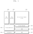
- FIG. 1 is a block diagram illustrating an image sensor according to some example embodiments of the inventive concepts.
- FIG. 2 is a circuit diagram illustrating an active pixel sensor array of an image sensor according to some example embodiments of the inventive concepts.
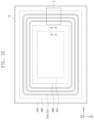
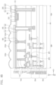
- FIG. 3 A is a plan view illustrating an image sensor according to some example embodiments of the inventive concepts.
- FIG. 3 B is an enlarged view of a region ‘A’ of FIG. 3 A .
- FIG. 3 C is a cross-sectional view taken along a line B-B′ of FIG. 3 A .
- FIG. 3 D is a cross-sectional view taken along a line C-C′ of FIG. 3 B .
- FIG. 3 E is a perspective view illustrating a lens layer of the image sensor of FIG. 3 A .
- FIG. 4 A is a plan view illustrating an image sensor according to some example embodiments of the inventive concepts.
- FIG. 4 B is a cross-sectional view taken along a line D-D′ of FIG. 4 A .
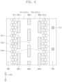
- FIG. 5 is a plan view illustrating an image sensor according to some example embodiments of the inventive concepts.
- FIG. 6 is a plan view illustrating an image sensor according to some example embodiments of the inventive concepts.
- FIG. 7 is a cross-sectional view illustrating an image sensor package according to some example embodiments of the inventive concepts.
- FIGS. 8 A and 8 B are cross-sectional views illustrating an image sensor according to some example embodiments of the inventive concepts.
- FIG. 9 is a cross-sectional view illustrating an image sensor according to some example embodiments of the inventive concepts.
- FIG. 1 is a block diagram illustrating an image sensor according to some example embodiments of the inventive concepts.
- FIG. 2 is a circuit diagram illustrating an active pixel sensor array of an image sensor according to some example embodiments of the inventive concepts.
- an image sensor may include an active pixel sensor array 1001 , a row decoder 1002 , a row driver 1003 , a column decoder 1004 , a timing generator 1005 , a correlated double sampler (CDS) 1006 , an analog-to-digital converter (ADC) 1007 , and an input/output (I/O) buffer 1008 .
- CDS correlated double sampler
- ADC analog-to-digital converter
- I/O input/output
- the active pixel sensor array 1001 may include a plurality of unit pixels two-dimensionally arranged and may convert optical signals into electrical signals.
- the active pixel sensor array 1001 may be driven by a plurality of driving signals (e.g., a pixel selection signal, a reset signal, and a charge transfer signal) provided from the row driver 1003 .
- the converted electrical signals may be provided to the correlated double sampler 1006 .
- the row driver 1003 may provide a plurality of driving signals for driving a plurality of the unit pixels to the active pixel sensor array 1001 in response to signals decoded in the row decoder 1002 .
- the driving signals may be provided in the unit of row of the matrix.
- the timing generator 1005 may provide timing signals and control signals to the row decoder 1002 and the column decoder 1004 .
- the correlated double sampler 1006 may receive electrical signals generated from the active pixel sensor array 1001 and may hold and sample the received electrical signals.
- the correlated double sampler 1006 may doubly sample a specific noise level and a signal level of the electrical signal to output a difference level corresponding to a difference between the noise level and the signal level.
- the analog-to-digital converter 1007 may convert an analog signal, which corresponds to the difference level outputted from the correlated double sampler 1006 , into a digital signal and may output the digital signal.
- the I/O buffer 1008 may latch the digital signals, and the latched signals may be sequentially outputted to an image signal processing unit (not shown) in response to signals decoded in the column decoder 1004 .
- the active pixel sensor array 1001 may include a plurality of unit pixels UP, and the unit pixels UP may be arranged in a matrix form.
- Each of the unit pixels UP may include a transfer transistor TX.
- Each of the unit pixels UP may further include logic transistors RX, SX and DX.
- the logic transistors RX, SX and DX may include a reset transistor RX, a selection transistor SX, and a source follower transistor DX.
- the transfer transistor TX may include a transfer gate TG.
- Each of the unit pixels UP may further include a photoelectric conversion portion PD and a floating diffusion region FD.
- the logic transistors RX, SX and DX may be shared by a plurality of the unit pixels UP.
- the photoelectric conversion portion PD may generate and accumulate photocharges in proportion to the amount of light incident from the outside.
- the photoelectric conversion portion PD may include a photodiode, a photo transistor, a photo gate, a pinned photodiode, or a combination thereof.
- the transfer transistor TX may transfer charges generated in the photoelectric conversion portion PD to the floating diffusion region FD.
- the floating diffusion region FD may receive the charges generated in the photoelectric conversion portion PD and may cumulatively store the received charges.
- the source follower transistor DX may be controlled according to the amount of the photocharges accumulated in the floating diffusion region PD.
- the reset transistor RX may periodically reset the charges accumulated in the floating diffusion region FD.
- a drain electrode of the reset transistor RX may be connected to the floating diffusion region PD, and a source electrode of the reset transistor RX may be connected to a power voltage V DD .
- V DD the power voltage connected to the source electrode of the reset transistor RX
- the reset transistor RX is turned-on, the charges accumulated in the floating diffusion region FD may be discharged to reset the floating diffusion region FD.
- the source follower transistor DX including a source follower gate electrode SF may function as a source follower buffer amplifier.
- the source follower transistor DX may amplify a potential change in the floating diffusion region FD and may output the amplified potential change to an output line Y OUT .
- the selection transistor SX including a selection gate electrode SEL may select the unit pixels UP to be sensed in the unit of row.
- the power voltage V DD may be applied to a drain electrode of the source follower transistor DX.
- FIG. 3 A is a plan view illustrating an image sensor according to some example embodiments of the inventive concepts.
- FIG. 3 B is an enlarged view of a region ‘A’ of FIG. 3 A .
- FIG. 3 C is a cross-sectional view taken along a line B-B′ of FIG. 3 A .
- FIG. 3 D is a cross-sectional view taken along a line C-C′ of FIG. 3 B .
- FIG. 3 E is a perspective view illustrating a lens layer of the image sensor of FIG. 3 A .
- an image sensor may include a sensor chip 10 .
- the sensor chip 10 may include a first substrate 100 .
- the first substrate 100 may have a plate shape extending along a plane defined by a first direction D 1 and a second direction D 2 .
- the first direction D 1 and the second direction D 2 may intersect each other.
- the first direction D 1 and the second direction D 2 may be horizontal directions perpendicular to each other.
- the first substrate 100 may be a semiconductor substrate.
- the first substrate 100 may be a silicon substrate, a germanium substrate, and/or a silicon-germanium substrate.
- the first substrate 100 may include dopants having a first conductivity type.
- the first substrate 100 may include aluminum (Al), boron (B), indium (In) and/or gallium (Ga) as the dopants having the first conductivity type.
- the first substrate 100 may be a silicon-on-insulator (SDI) substrate.
- SDI silicon-on-insulator
- the first substrate 100 may include a pixel array region APS, a dummy region DMR, an optical black region OBR, and a pad region PDR.
- the pixel array region APS, the dummy region DMR, the optical black region OBR and the pad region PDR may be regions divided when viewed in a plan view defined by the first direction D 1 and the second direction D 2 .
- the dummy region DMR may surround the pixel array region APS
- the optical black region OBR may surround the dummy region DMR and the pixel array region APS
- the pad region PDR may surround the optical black region OBR, the dummy region DMR and the pixel array region APS.
- the first substrate 100 may have a front surface and a back surface, which are opposite to each other. Light may be incident to the back surface of the first substrate 100 .
- the pixel array region APS of the first substrate 100 may include a plurality of pixel regions PX.
- the pixel region PX of the pixel array region APS may output a photoelectric signal from incident light.
- the pixel regions PX may be two-dimensionally arranged in the pixel array region APS.
- the dummy region DMR of the first substrate 100 may include a plurality of pixel regions PX.
- the pixel regions PX of the dummy region DMR may be dummy pixel regions.
- the first substrate 100 may include a plurality of photoelectric conversion regions PD.
- the photoelectric conversion regions PD may be disposed between the front surface and the back surface of the first substrate 100 .
- the photoelectric conversion regions PD may be provided in the pixel regions PX of the first substrate 100 , respectively.
- the photoelectric conversion region PD may include dopants having a second conductivity type.
- the second conductivity type may be different from the first conductivity type.
- the photoelectric conversion region PD may include phosphorus, arsenic, bismuth and/or antimony as the dopants having the second conductivity type.
- the photoelectric conversion region PD may be adjacent to the back surface of the first substrate 100 .
- the first substrate 100 may include a plurality of floating diffusion regions FD.
- the floating diffusion regions FD may be provided in the pixel regions PX of the first substrate 100 , respectively.
- the floating diffusion regions PD may include dopants having the second conductivity type.
- the floating diffusion region FD may be adjacent to the front surface of the first substrate 100 .
- the sensor chip 10 may include a pixel isolation pattern 110 .
- the pixel isolation pattern 110 may be provided in the first substrate 100 .
- the pixel isolation pattern 110 may extend in a third direction D 3 to penetrate the first substrate 100 .
- the third direction D 3 may intersect the first direction D 1 and the second direction D 2 .
- the third direction D 3 may be a vertical direction perpendicular to the first direction D 1 and the second direction D 2 .
- the pixel regions PX may be defined by the pixel isolation pattern 110 .
- the pixel isolation pattern 110 may have a grid shape when viewed in a plan view.
- the pixel isolation pattern 110 may include an isolation conductive layer 111 and an isolation insulating layer 112 .
- the isolation conductive layer 111 may penetrate the first substrate 100 .
- the isolation insulating layer 112 may be disposed between the isolation conductive layer 111 and the first substrate 100 .
- the isolation conductive layer 111 may include a conductive material.
- the isolation insulating layer 112 may include an insulating material.
- the sensor chip 10 may include a device isolation pattern 120 .
- the device isolation pattern 120 may be provided in the first substrate 100 .
- the device isolation pattern 120 may be disposed adjacent to the front surface of the first substrate 100 .
- the device isolation pattern 120 may define an active region of the first substrate 100 .
- the device isolation pattern 120 may include an insulating material.
- the sensor chip 10 may include a first interconnection insulating layer 130 covering the front surface of the first substrate 100 .
- the first interconnection insulating layer 130 may cover the active region of the first substrate 100 .
- the first interconnection insulating layer 130 may include an insulating material.
- the first interconnection insulating layer 130 may be a multi-insulating layer including a plurality of insulating layers.
- the sensor chip 10 may include transfer gates TG and gate insulating layers GI.
- the transfer gate TG may be provided between the first substrate 100 and the first interconnection insulating layer 130 .
- the transfer gate TG may include a conductive material.
- the gate insulating layer GI may be provided between the transfer gate TG and the first substrate 100 .
- the gate insulating layer GI may include an insulating material.
- First contacts CT 1 and first conductive lines CL 1 may be provided in the first interconnection insulating layer 130 . At least some of the first contacts CT 1 may be connected to the floating diffusion regions FD. At least some of the first conductive lines CL 1 may be connected to the at least some first contacts CT 1 .
- the first contacts CT 1 and the first conductive lines CL 1 may include a conductive material.
- the sensor chip 10 may include a fixed charge layer 140 covering the back surface of the first substrate 100 .
- the fixed charge layer 140 may be a metal oxide layer including insufficient oxygen in terms of a stoichiometric ratio or a metal fluoride layer including insufficient fluorine in terms of a stoichiometric ratio.
- the fixed charge layer 140 may have negative fixed charges and may accumulate holes. A dark current and a white spot of the first substrate 100 may be effectively reduced by the fixed charge layer 140 .
- the fixed charge layer 140 may include a plurality of different layers.
- the sensor chip 10 may include an anti-reflection layer 150 on the fixed charge layer 140 .
- the anti-reflection layer 150 may include aluminum oxide.
- the anti-reflection layer 150 may include a plurality of different layers.
- the sensor chip 10 may include a fence pattern 160 on the anti-reflection layer 150 .
- the fence pattern 160 may be disposed over the pixel array region APS of the first substrate 100 .
- the fence pattern 160 may divide color filters CF to be described later from each other.
- the fence pattern 160 may have a grid shape when viewed in a plan view.
- the fence pattern 160 may include a conductive material.
- the fence pattern 160 may include tungsten.
- the sensor chip 10 may include a light blocking layer 170 on the anti-reflection layer 150 .
- the light blocking layer 170 may be disposed over the dummy region DMR, the optical black region OBR and the pad region PDR of the first substrate 100 .
- the light blocking layer 170 may include a conductive material.
- the light blocking layer 170 may include the same material as the fence pattern 160 .
- the light blocking layer 170 may include tungsten.
- the sensor chip 10 may include a protective layer covering the fence pattern 160 and the light blocking layer 170 .
- the protective layer may include an insulating material.
- the sensor chip 10 may include a connection contact 180 .
- the connection contact 180 may be disposed over the optical black region OBR of the first substrate 100 .
- the connection contact 180 may penetrate the fixed charge layer 140 and the anti-reflection layer 150 so as to be connected to the pixel isolation pattern 110 .
- the connection contact 180 may include a first contact pattern 181 connected to the pixel isolation pattern 110 , and a second contact pattern 182 on the first contact pattern 181 .
- the first contact pattern 181 may be connected to the light blocking layer 170 without an interface therebetween (e.g., may directly contact).
- the first contact pattern 181 and the light blocking layer 170 may constitute a single body structure.
- the first contact pattern 181 may include the same material as the light blocking layer 170 .
- the second contact pattern 182 may include a different material from that of the first contact pattern 181 .
- the second contact pattern 182 may include aluminum.
- the sensor chip 10 may include a first connection structure 190 .
- the first connection structure 190 may be disposed over the optical black region OBR of the first substrate 100 .
- the first connection structure 190 may penetrate the fixed charge layer 140 , the anti-reflection layer 150 , the first substrate 100 and the first interconnection insulating layer 130 so as to be connected to a circuit chip 20 to be described later.
- the first connection structure 190 may be connected to at least one of the first conductive lines CL 1 in the first interconnection insulating layer 130 .
- the first connection structure 190 may include a first conductive pattern 191 connected to the circuit chip 20 , a first insulating pattern 192 on the first conductive pattern 191 , and a first capping pattern 193 on the first insulating pattern 192 .
- the first conductive pattern 191 may be connected to the light blocking layer 170 without an interface therebetween (e.g., may directly contact).
- the first conductive pattern 191 and the light blocking layer 170 may constitute a single body structure.
- the first conductive pattern 191 may include the same material as the light blocking layer 170 .
- the first insulating pattern 192 may include an insulating material.
- the first capping pattern 193 may include an insulating material.
- the sensor chip 10 may include a conductive pad 210 .
- the conductive pad 210 may be disposed over the pad region PDR of the first substrate 100 .
- the conductive pad 210 may penetrate the fixed charge layer 140 and the anti-reflection layer 150 so as to be connected to the first substrate 100 .
- the conductive pad 210 may include a first pad pattern 211 on the first substrate 100 and a second pad pattern 212 on the first pad pattern 211 .
- the first pad pattern 211 may be connected to the light blocking layer 170 without an interface therebetween (e.g., may directly contact).
- the first pad pattern 211 and the light blocking layer 170 may constitute a single body structure.
- the first pad pattern 211 may include the same material as the light blocking layer 170 .
- the second pad pattern 212 may include a different material from that of the first pad pattern 211 .
- the second pad pattern 212 may include aluminum.
- the sensor chip 10 may include a second connection structure 220 .
- the second connection structure 220 may be disposed over the pad region PDR of the first substrate 100 .
- the second connection structure 220 may penetrate the fixed charge layer 140 , the anti-reflection layer 150 , the first substrate 100 and the first interconnection insulating layer 130 so as to be connected to the circuit chip 20 to be described later in detail.
- the second connection structure 220 may be connected to at least one of the first conductive lines CL 1 in the first interconnection insulating layer 130 .
- the second connection structure 220 may include a second conductive pattern 221 connected to the circuit chip 20 , a second insulating pattern 222 on the second conductive pattern 221 , and a second capping pattern 223 on the second insulating pattern 222 .
- the second conductive pattern 221 may be connected to the light blocking layer 170 without an interface therebetween (e.g., may directly contact).
- the second conductive pattern 221 and the light blocking layer 170 may constitute a single body structure.
- the second conductive pattern 221 may include the same material as the light blocking layer 170 .
- the second insulating pattern 222 may include an insulating material.
- the second capping pattern 223 may include an insulating material.
- the sensor chip 10 may include the color filters CF.
- the color filters CF may be disposed over the pixel array region APS and the dummy region DMR of the first substrate 100 .
- the color filters CF may be disposed over the pixel regions PX, respectively.
- the color filters CF may be provided at positions corresponding to the photoelectric conversion regions PD, respectively.
- Each of the color filters CF may be a red filter, a blue filter, or a green filter.
- the color filters CF may constitute a color filter array.
- the color filters CF may be two-dimensionally arranged in the form of a Bayer pattern. However, other color filters (e.g., a cyan filter, a magenta filter, and/or a yellow filter) and patterns may be used.
- the fence pattern 160 may be provided between the color filters CF disposed over the pixel array region APS.
- the color filters CF disposed over the dummy region DMR may be provided on the light blocking layer 170 .
- the color filters CF disposed over the dummy region DMR may be dummy color filters.
- the sensor chip 10 may include a black bulk filtering layer FI.
- the black bulk filtering layer FI may be disposed over the optical black region OBR of the first substrate 100 .
- the black bulk filtering layer FI may be disposed on the light blocking layer 170 .
- the black bulk filtering layer FI may block light having a wavelength different from those of the color filters CF.
- the sensor chip 10 may include a lens layer 230 .
- the lens layer 230 may be disposed over the pixel array region APS, the dummy region DMR, the optical black region OBR and the pad region PDR of the first substrate 100 .
- the lens layer 230 may be disposed on the color filters CF and the black bulk filtering layer FI.
- the lens layer 230 may be transparent.
- the lens layer 230 may transmit light.
- the lens layer 230 may include an organic material.
- the lens layer 230 may include a photoresist material and/or a thermosetting resin.
- the lens layer 230 may include a base portion 231 on the color filters CF and the black bulk filtering layer FI.
- the lens layer 230 may include micro lenses 232 , dummy lenses 233 and blocking bars 234 on the base portion 231 .
- the micro lenses 232 , the dummy lenses 233 and the blocking bars 234 may be disposed at the same level.
- the micro lenses 232 , the dummy lenses 233 and the blocking bars 234 may be portions protruding from the base portion 231 in the third direction D 3 .
- the micro lenses 232 , the dummy lenses 233 and the blocking bars 234 may be connected to the base portion 231 without interfaces therebetween.
- the micro lenses 232 , the dummy lenses 233 , the blocking bars 234 and the base portion 231 may constitute a single body structure.
- the micro lenses 232 may be disposed over the pixel array region APS and the dummy region DMR of the first substrate 100 .
- the dummy lenses 233 and the blocking bars 234 may be disposed over the optical black region OBR of the first substrate 100 .
- the micro lenses 232 may be disposed over the pixel regions PX, respectively.
- the micro lenses 232 may be provided at positions corresponding to the photoelectric conversion regions PD, respectively.
- the micro lenses 232 disposed over the dummy region DMR may be dummy micro lenses.
- the blocking bar 234 may include two portions extending in the first direction D 1 and two portions extending in the second direction D 2 .
- the blocking bar 234 may surround the micro lenses 232 when viewed in a plan view.
- the micro lenses 232 may be disposed between the two portions, extending in the first direction D 1 , of the blocking bar 234 .
- the micro lenses 232 may be disposed between the two portions, extending in the second direction D 2 , of the blocking bar 234 .
- the blocking bar 234 may surround at least some of the dummy lenses 233 when viewed in a plan view. In the plan view of FIG. 3 A , the blocking bar 234 may have a ring shape.
- a length of the blocking bar 234 may be greater than a length of the micro lens 232 and a length of the dummy lens 233 .
- a length, in the first direction D 1 of the portion extending in the first direction D 1 of the blocking bar 234 may be greater than a length of the micro lens 232 in the first direction D 1 and a length of the dummy lens 233 in the first direction D 1 .
- the length of the blocking bar 234 may be greater than a length of the pixel array region APS of the first substrate 100 . The length may be measured in the direction the blocking bar 234 extends furthest, e.g., either the first direction D 1 , or the second direction D 2 , based on the location being considered in the sensor chip 10 .
- a top surface 232 t of the micro lens 232 , a top surface 233 t of the dummy lens 233 and a top surface 234 t of the blocking bar 234 may be curved.
- a curvature radius of the top surface 232 t of the micro lens 232 , a curvature radius of the top surface 233 t of the dummy lens 233 and a curvature radius of the top surface 234 t of the blocking bar 234 may be equal to each other. For example, in the cross-sectional views of FIGS.
- the curvature radius of the top surface 232 t of the micro lens 232 , the curvature radius of the top surface 233 t of the dummy lens 233 and the curvature radius of the top surface 234 t of the blocking bar 234 may be equal to each other.
- the curvature radius of the top surface 232 t of the micro lens 232 , the curvature radius of the top surface 233 t of the dummy lens 233 and the curvature radius of the top surface 234 t of the blocking bar 234 may be different from each other.
- a maximum width of the micro lens 232 , a maximum width of the dummy lens 233 and a maximum width of the blocking bar 234 may be equal to each other.
- a maximum width W 1 of the micro lens 232 in the first direction D 1 a maximum width W 2 of the dummy lens 233 in the first direction D 1 and a maximum width W 3 of the blocking bar 234 in the first direction D 1 may be equal to each other.
- the maximum width of the micro lens 232 , the maximum width of the dummy lens 233 and the maximum width of the blocking bar 234 may be different from each other.
- An uppermost level of the micro lens 232 , an uppermost level of the dummy lens 233 and an uppermost level of the blocking bar 234 may be the same as each other. In some example embodiments, the uppermost level of the micro lens 232 , the uppermost level of the dummy lens 233 and the uppermost level of the blocking bar 234 may be different from each other.
- the sensor chip 10 may include a coating layer 240 on the lens layer 230 .
- the coating layer 240 may be transparent.
- the coating layer 240 may conformally cover a top surface of the lens layer 230 .
- the coating layer 240 may include a first portion on the micro lens 232 , a second portion on the dummy lens 233 , and a third portion on the blocking bar 234 . Top surfaces of the first, second and third portions of the coating layer 240 may be curved.
- a recess RS penetrating the coating layer 240 and the lens layer 230 may be defined.
- the conductive pad 210 may be exposed by the recess RS.
- the recess RS may be defined by sidewalls of the coating layer 240 and the lens layer 230 and upper surfaces of conductive pad 210 .
- the image sensor may include the circuit chip 20 .
- the circuit chip 20 may include a second substrate 300 .
- the second substrate 300 may be a semiconductor substrate.
- the second substrate 300 may be a SDI substrate.
- the circuit chip 20 may include a second interconnection insulating layer 310 on the second substrate 300 .
- the second interconnection insulating layer 310 may cover an active region of the second substrate 300 .
- the second interconnection insulating layer 310 may include an insulating material.
- the second interconnection insulating layer 310 may be a multi-insulating layer including a plurality of insulating layers.
- the circuit chip 20 may include integrated circuits 320 between the second substrate 300 and the second interconnection insulating layer 310 .
- the integrated circuits 320 may include at least one of a logic circuit or a memory circuit.
- the circuit chip 20 may include second contacts CT 2 and second conductive lines CL 2 in the second interconnection insulating layer 310 . At least some of the second contacts CT 2 may be connected to the integrated circuits 320 . At least some of the second conductive lines CL 2 may be connected to the at least some second contacts CT 2 . At least one of the second conductive lines CL 2 may be connected to the first connection structure 190 . At least one of the second conductive lines CL 2 may be connected to the second connection structure 220 .
- the second contacts CT 2 and the second conductive lines CL 2 may include a conductive material.
- the dummy lenses 233 may include first dummy lenses DL 1 , second dummy lenses DL 2 , third dummy lenses DL 3 , and fourth dummy lenses DL 4 .
- the blocking bars 234 may include a first blocking bar BB 1 , a second blocking bar BB 2 , and a third blocking bar BB 3 .
- the number of the blocking bars 234 is not limited to 3. In some example embodiments, the number of the blocking bars 234 may be 2 or less or may be 4 or more.
- the first blocking bar BB 1 may surround the first dummy lenses DL 1 and the micro lenses 232 when viewed in a plan view.
- the second blocking bar BB 2 may surround the first blocking bar BB 1 , the second dummy lenses DL 2 , the first dummy lenses DL 1 and the micro lenses 232 when viewed in a plan view.
- the third blocking bar BB 3 may surround the second blocking bar BB 2 , the third dummy lenses DL 3 , the first blocking bar BB 1 , the second dummy lenses DL 2 , the first dummy lenses DL 1 and the micro lenses 232 when viewed in a plan view.
- a distance between the first dummy lens DL 1 and the micro lens 232 may be less than a distance between the first blocking bar BB 1 and the micro lens 232 .
- the second dummy lens DL 2 may be disposed between the first and second blocking bars BB 1 and BB 2 .
- the third dummy lens DL 3 may be disposed between the second and third blocking bars BB 2 and BB 3 .
- a distance between the fourth dummy lens DL 4 and the micro lens 232 may be greater than a distance between the third blocking bar BB 3 and the micro lens 232 .
- the first to third blocking bars BB 1 , BB 2 and BB 3 may be disposed between the first dummy lens DL 1 and the fourth dummy lens DL 4 .
- the first to third blocking bars BB 1 to BB 3 may have a concentric ring pattern (e.g., the first blocking bar BB 1 may be a first, smaller ring, the second blocking bar BB 2 may be a larger ring surrounding the first blocking bar BB 1 , and the third blocking bar BB 3 may be the largest ring, surrounding the second blocking bar BB 2 ).
- the first to third blocking bars BB 1 to BB 3 may have a different shape, and in some example embodiments, the blocking bars BB 1 to BB 3 may have the same or different types of shapes (e.g., rings, circles, etc.).
- a method of manufacturing an image sensor package including the image sensor may include applying an adhesive material over the pad region PDR of the first substrate 100 of the image sensor, and forming a dam structure on the adhesive material.
- the adhesive material may include an epoxy.
- the blocking bar 234 is provided over the optical black region OBR, it is possible to prevent or reduce the adhesive material applied over the pad region PDR from permeating to the pixel array region APS, and it is possible to prevent or reduce sensitivity of the image sensor from being deteriorated.
- Compressive stress may be generated in the blocking bar 234 of the image sensor according to some example embodiments, and the compressive stress of the blocking bar 234 may prevent or reduce the occurrence of a crack of the coating layer 240 occurring over the optical black region OBR from propagating onto the pixel array region APS.
- FIG. 4 A is a plan view illustrating an image sensor according to some example embodiments of the inventive concepts.
- FIG. 4 B is a cross-sectional view taken along a line D-D′ of FIG. 4 A .
- an image sensor may include a sensor chip 10 a and a circuit chip 20 a .
- the sensor chip 10 a may include a lens layer 230 a.
- the lens layer 230 a may include a base portion 231 a .
- the lens layer 230 a may include first dummy lenses DL 1 a , second dummy lenses DL 2 a , a first blocking bar BB 1 a , a second blocking bar BB 2 a and a third blocking bar BB 3 a on the base portion 231 a.
- the first dummy lenses DL 1 a may be surrounded by the first to third blocking bars BB 1 a , BB 2 a and BB 3 a when viewed in a plan view.
- the second dummy lenses DL 2 a may be closer to the pad region PDR than the third blocking bar BB 3 a .
- the dummy lens may not be disposed between the first and second blocking bars BB 1 a and BB 2 a .
- the dummy lens may not be disposed between the second and third blocking bars BB 2 a and BB 3 a.
- the first to third blocking bars BB 1 a to BB 3 a may have a concentric ring pattern (e.g., the first blocking bar BB 1 a may be a first, smaller ring, the second blocking bar BB 2 a may be a larger ring surrounding the first blocking bar BB 1 a , and the third blocking bar BB 3 a may be the largest ring, surrounding the second blocking bar BB 2 a ).
- the first to third blocking bars BB 1 b to BB 3 b may or may not have a bar at the corner intersections of the first to third blocking bars BB 1 b to BB 3 b in the first and second directions D 1 and D 2 .
- the base portion 231 a may include a first flat top surface FS 1 a between the first and second blocking bars BB 1 a and BB 2 a and a second flat top surface FS 2 a between the second and third blocking bars BB 2 a and BB 3 a.
- the first flat top surface FS 1 a may connect the first blocking bar BB 1 a and the second blocking bar BB 2 a .
- the first flat top surface FS 1 a may be flat.
- the first flat top surface FS 1 a may include two portions extending in the first direction D 1 and two portions extending in the second direction D 2 .
- the first flat top surface FS 1 a may have a ring shape when viewed in a plan view.
- a width of the first flat top surface FS 1 a may be greater than a width of the first blocking bar BB 1 a and a width of the second blocking bar BB 2 a .
- a width, in the first direction D 1 , of the portion extending in the second direction D 2 of the first flat top surface FS 1 a may be greater than a width, in the first direction D 1 , of a portion extending in the second direction D 2 of the first blocking bar BB 1 a and a width, in the first direction D 1 , of a portion extending in the second direction D 2 of the second blocking bar BB 2 a.
- the second flat top surface FS 2 a may connect the second blocking bar BB 2 a and the third blocking bar BB 3 a .
- the second flat top surface FS 2 a may be flat.
- the second flat top surface FS 2 a may include two portions extending in the first direction D 1 and two portions extending in the second direction D 2 .
- the second flat top surface FS 2 a may have a ring shape when viewed in a plan view.
- a width of the second flat top surface FS 2 a may be greater than the width of the second blocking bar BB 2 a and a width of the third blocking bar BB 3 a .
- a width, in the first direction D 1 , of the portion extending in the second direction D 2 of the second flat top surface FS 2 a may be greater than the width, in the first direction D 1 , of the portion extending in the second direction D 2 of the second blocking bar BB 2 a and a width, in the first direction D 1 , of a portion extending in the second direction D 2 of the third blocking bar BB 3 a.
- FIG. 5 is a plan view illustrating an image sensor according to some example embodiments of the inventive concepts.
- an image sensor may include first dummy lenses DL 1 b , second dummy lenses DL 2 b , third dummy lenses DL 3 b , fourth dummy lenses DL 4 b , first blocking bars BB 1 b , second blocking bars BB 2 b , and third blocking bars BB 3 b.
- the first blocking bars BB 1 b may be spaced apart from each other.
- the first blocking bars BB 1 b may include the first blocking bars BB 1 b extending in the first direction D 1 and the first blocking bars BB 1 b extending in the second direction D 2 .
- the first blocking bars BB 1 b extending in the first direction D 1 may be arranged in the first direction D 1 .
- the first blocking bars BB 1 b extending in the second direction D 2 may be arranged in the second direction D 2 .
- the second blocking bars BB 2 b may be spaced apart from each other.
- the second blocking bars BB 2 b may include the second blocking bars BB 2 b extending in the first direction D 1 and the second blocking bars BB 2 b extending in the second direction D 2 .
- the second blocking bars BB 2 b extending in the first direction D 1 may be arranged in the first direction D 1 .
- the second blocking bars BB 2 b extending in the second direction D 2 may be arranged in the second direction D 2 .
- the third blocking bars BB 3 b may be spaced apart from each other.
- the third blocking bars BB 3 b may include the third blocking bars BB 3 b extending in the first direction D 1 and the third blocking bars BB 3 b extending in the second direction D 2 .
- the third blocking bars BB 3 b extending in the first direction D 1 may be arranged in the first direction D 1 .
- the third blocking bars BB 3 b extending in the second direction D 2 may be arranged in the second direction D 2 .
- the first to third blocking bars BB 1 b to BB 3 b may have a concentric ring pattern (e.g., the first blocking bars BB 1 b may be a first, smaller ring, the second blocking bars BB 2 b may be a larger ring surrounding the first blocking bars BB 1 b , and the third blocking bars BB 3 b may be the largest ring, surrounding the second blocking bars BB 2 b ).
- the first to third blocking bars BB 1 b to BB 3 b may or may not have a bar at the corner intersections of the first to third blocking bars BB 1 b to BB 3 b in the first and second directions D 1 and D 2 .
- a first gap GA 1 b may be defined between the first blocking bars BB 1 b adjacent to each other.
- a second gap GA 2 b may be defined between the second blocking bars BB 2 b adjacent to each other.
- a third gap GA 3 b may be defined between the third blocking bars BB 3 b adjacent to each other. Portions of a top surface of the base portion 231 b may be exposed by the first to third gaps GA 1 b , GA 2 b and GA 3 b.
- a width of the gap GA 1 b , GA 2 b or GA 3 b may be equal to a width of the blocking bar BB 1 b , BB 2 b or BB 3 b .
- a width, in the first direction D 1 , of the first gap GA 1 b provided between the first blocking bars BB 1 b extending in the second direction D 2 may be equal to a width, in the first direction D 1 , of the first blocking bar BB 1 b extending in the second direction D 2 .
- a length of the blocking bar BB 1 b , BB 2 b or BB 3 b may be greater than a length of the gap GA 1 b , GA 2 b or GA 3 b .
- a length, in the second direction D 2 , of the first blocking bar BB 1 b extending in the second direction D 2 may be greater than a length, in the second direction D 2 , of the first gap GA 1 b provided between the first blocking bars BB 1 b extending in the second direction D 2 .
- FIG. 6 is a plan view illustrating an image sensor according to some example embodiments of the inventive concepts.
- an image sensor may include first blocking bars BB 1 c , second blocking bars BB 2 c , third blocking bars BB 3 c , first dummy lenses DL 1 c surrounded by the first blocking bars BB 1 c in a plan view, and second dummy lenses DL 2 c surrounding the third blocking bars BB 3 c in a plan view.
- the first to third blocking bars BB 1 c to BB 3 c may have a concentric ring pattern (e.g., the first blocking bars BB 1 c may be a first, smaller ring, the second blocking bars BB 2 c may be a larger ring surrounding the first blocking bars BB 1 c , and the third blocking bars BB 3 c may be the largest ring, surrounding the second blocking bars BB 2 c ).
- First gaps GA 1 c may be defined between the first blocking bars BB 1 c
- second gaps GA 2 c may be defined between the second blocking bars BB 2 c
- third gaps GA 3 c may be defined between the third blocking bars BB 3 c.
- a base portion 231 c may include a first flat top surface FS 1 c between the first blocking bars BB 1 c and the second blocking bars BB 2 c and a second flat top surface FS 2 c between the second blocking bars BB 2 c and the third blocking bars BB 3 c .
- the first flat top surface FS 1 c may be connected to the first and second gaps GA 1 c and GA 2 c .
- the second flat top surface FS 2 c may be connected to the second and third gaps GA 2 c and GA 3 c.
- FIG. 7 is a cross-sectional view illustrating an image sensor package according to some example embodiments of the inventive concepts.
- an image sensor package may include a package substrate 410 .
- the package substrate 410 may be a printed circuit board (PCB).
- the package substrate 410 may include upper pads 430 .
- the upper pads 430 may include a conductive material.
- External connection terminals 420 may be provided under the package substrate 410 .
- the image sensor package may be electrically connected to an external device through the external connection terminals 420 .
- the external connection terminals 420 may include a conductive material.
- An adhesive layer 440 may be provided on the package substrate 410 .
- the adhesive layer 440 may include a polymer material.
- An image sensor 450 may be provided on the adhesive layer 440 .
- the image sensor 450 may include a pixel array region 451 , an optical black region 452 , and a pad region 453 .
- the image sensor 450 may include a conductive pad 454 in the pad region 453 .
- the conductive pad 454 may be electrically connected to the upper pad 430 through a wire.
- the image sensor 450 may include a sensor chip and a circuit chip, and the conductive pad 454 may be provided between the sensor chip and the circuit chip of the image sensor 450 so as to be connected directly to the circuit chip.
- a micro lens may be provided in the pixel array region 451 of the image sensor 450 .
- a dummy lens and a blocking bar may be provided in the optical black region 452 of the image sensor 450 .
- a dam structure 480 may be provided on a portion of the optical black region 452 and the pad region 453 of the image sensor 450 .
- the image sensor 450 may be provided on only the pad region 453 .
- the dam structure 480 may be adhered to the image sensor 450 by using an adhesive material (not shown).
- the pixel array region 451 of the image sensor 450 may be exposed by the dam structure 480 .
- the dam structure 480 may include at least one of a polymer material or a metal.
- the dam structure 480 may have a ring shape when viewed in a plan view.
- a transparent substrate 490 may be provided on the dam structure 480 .
- the transparent substrate 490 may include a material having a high light transmittance.
- the transparent substrate 490 may include glass.
- a molding layer 470 may be provided to surround the transparent substrate 490 , the dam structure 480 and the image sensor 450 .
- the molding layer 470 may include a polymer material.
- the image sensor 450 includes the blocking bar in the image sensor package according to some example embodiments, it is possible to prevent or reduce the adhesive material for adhering the dam structure 480 to the image sensor 450 from permeating to the pixel array region 451 , and it is possible to prevent or reduce sensitivity of the image sensor 450 from being deteriorated.
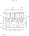
- FIGS. 8 A and 8 B are cross-sectional views illustrating an image sensor according to some example embodiments of the inventive concepts.
- an image sensor may include a sub-chip 20 d , a circuit chip 30 d , and a sensor chip 10 d .
- the sub-chip 20 d may be provided on the circuit chip 30 d
- the sensor chip 10 d may be provided on the sub-chip 20 d .
- the sensor chip 10 d may include micro lenses 231 d , dummy lenses 232 d , and a blocking bar 233 d.
- the sensor chip 10 d may include a first substrate 100 and a first interconnection insulating layer 130 d .
- the sub-chip 20 d may include a second substrate 300 d and a second interconnection insulating layer 310 d .
- the circuit chip 30 d may include a third substrate 500 d and a third interconnection insulating layer 510 d .
- the first interconnection insulating layer 130 d may be in contact with the second interconnection insulating layer 310 d .
- the second substrate 300 d may be in contact with the third interconnection insulating layer 510 d.
- the sensor chip 10 d may include a first bonding pad BP 1 being in contact with the sub-chip 20 d .
- the sub-chip 20 d may include a second bonding pad BP 2 being in contact with the first bonding pad BP 1 .
- the sensor chip 10 d and the sub-chip 20 d may be electrically connected to each other through the first and second bonding pads BP 1 and BP 2 .
- the first and second bonding pads BP 1 and BP 2 may include copper.
- the sub-chip 20 d may include an electronic device 320 d , first contacts 330 d connected to the electronic device 320 d , and a first conductive line 340 d .
- the first contact 330 d may be connected to the first conductive line 340 d or the second bonding pad BP 2 .
- the electronic device 320 d may include at least one of a selection transistor, a reset gate, or a source follower gate.
- the first contact 330 d and the first conductive line 340 d may be provided in the second interconnection insulating layer 310 d.
- the circuit chip 30 d may include an integrated circuit 520 d , a second contact 530 d connected to the integrated circuit 520 d , and a second conductive line 540 d connected to the second contact 530 d .
- the second contact 530 d and the second conductive line 540 d may be provided in the third interconnection insulating layer 510 d.
- a through-via TV may be provided.
- the through-via TV may penetrate the second substrate 300 d of the sub-chip 20 d .
- the through-via TV may be connected to the first conductive line 340 d and the second conductive line 540 d .
- the sub-chip 20 d and the circuit chip 30 d may be electrically connected to each other through the through-via TV.
- the through-via TV may include a conductive material.
- FIG. 9 is a cross-sectional view illustrating an image sensor according to some example embodiments of the inventive concepts.
- an image sensor may include a sensor chip 10 e and a circuit chip 20 e .
- the sensor chip 10 e may include a base portion 231 e , dummy lenses 232 e , and a blocking bar 233 e.
- the image sensor may include a conductive pad 210 e connected directly to the circuit chip 20 e .
- the conductive pad 210 e may be provided in a recess RSe.
- the recess RSe may penetrate a lens layer 230 e , an anti-reflection layer 150 e , a fixed charge layer 140 e , a first substrate 100 e and a first interconnection insulating layer 130 e of the sensor chip 10 e to expose a conductive structure CSe in a second interconnection insulating layer 310 e of the circuit chip 20 e .
- the conductive pad 210 e may be connected directly to the conductive structure CSe in the second interconnection insulating layer 310 e of the circuit chip 20 e .
- the conductive pad 210 e may include a conductive material.
- the conductive structure CSe may include a conductive material.
- the conductive structure CSe may be a conductive line, a conductive contact, or a conductive pad.
- the image sensor of FIG. 1 may include hardware including logic circuits; a hardware/software combination such as a processor executing software; or a combination thereof.
- the processing circuitry more specifically may include, but is not limited to, a central processing unit (CPU), an arithmetic logic unit (ALU), a digital signal processor, a microcomputer, a field programmable gate array (FPGA), a System-on-Chip (SoC), a programmable logic unit, a microprocessor, application-specific integrated circuit (ASIC), etc.
- CPU central processing unit
- ALU arithmetic logic unit
- DSP digital signal processor
- microcomputer a field programmable gate array
- FPGA field programmable gate array
- SoC System-on-Chip
- ASIC application-specific integrated circuit
- the image sensor according to some example embodiments of the inventive concepts may include the blocking bar on the optical black region, thereby preventing or reducing the adhesive material applied on the optical black region from permeating to the pixel array region and preventing or reducing the sensitivity of the image sensor from being deteriorated.
Landscapes
- Solid State Image Pick-Up Elements (AREA)
Applications Claiming Priority (2)
| Application Number | Priority Date | Filing Date | Title |
|---|---|---|---|
| KR1020220104084A KR20240025897A (ko) | 2022-08-19 | 2022-08-19 | 이미지 센서 |
| KR10-2022-0104084 | 2022-08-19 |
Publications (1)
| Publication Number | Publication Date |
|---|---|
| US20240063243A1 true US20240063243A1 (en) | 2024-02-22 |
Family
ID=89906105
Family Applications (1)
| Application Number | Title | Priority Date | Filing Date |
|---|---|---|---|
| US18/300,009 Pending US20240063243A1 (en) | 2022-08-19 | 2023-04-13 | Image sensor |
Country Status (4)
| Country | Link |
|---|---|
| US (1) | US20240063243A1 (https=) |
| JP (1) | JP2024028099A (https=) |
| KR (1) | KR20240025897A (https=) |
| CN (1) | CN117594616A (https=) |
Cited By (1)
| Publication number | Priority date | Publication date | Assignee | Title |
|---|---|---|---|---|
| US20240186342A1 (en) * | 2022-12-02 | 2024-06-06 | SK Hynix Inc. | Image sensing device |
-
2022
- 2022-08-19 KR KR1020220104084A patent/KR20240025897A/ko active Pending
-
2023
- 2023-03-23 CN CN202310328788.8A patent/CN117594616A/zh active Pending
- 2023-04-13 US US18/300,009 patent/US20240063243A1/en active Pending
- 2023-04-19 JP JP2023068545A patent/JP2024028099A/ja active Pending
Cited By (1)
| Publication number | Priority date | Publication date | Assignee | Title |
|---|---|---|---|---|
| US20240186342A1 (en) * | 2022-12-02 | 2024-06-06 | SK Hynix Inc. | Image sensing device |
Also Published As
| Publication number | Publication date |
|---|---|
| CN117594616A (zh) | 2024-02-23 |
| JP2024028099A (ja) | 2024-03-01 |
| KR20240025897A (ko) | 2024-02-27 |
Similar Documents
| Publication | Publication Date | Title |
|---|---|---|
| KR101497715B1 (ko) | 고체 촬상 장치 및 카메라 | |
| US12170299B2 (en) | Image sensors | |
| US11031428B2 (en) | Image sensor | |
| US11637147B2 (en) | Imaging device | |
| US20100025791A1 (en) | Solid-state imaging device and method for manufacturing same | |
| KR20170043140A (ko) | 이미지 센서 | |
| KR101975028B1 (ko) | 이미지 센서 | |
| US8339488B2 (en) | Solid-state image pickup device having laminated color filters, manufacturing method thereof, and electronic apparatus incorporating same | |
| US12074180B2 (en) | Imaging element and method of manufacturing imaging element | |
| US20220344384A1 (en) | Image sensor | |
| US20250151434A1 (en) | Image sensor having pixels with different light receiving areas | |
| KR20200086389A (ko) | 이미지 센서 | |
| US20210335877A1 (en) | Image sensor and a method of fabricating the same | |
| US20240063243A1 (en) | Image sensor | |
| KR102864437B1 (ko) | 이미지 센서 | |
| US5444277A (en) | Solid imaging pick-up element | |
| US20260101603A1 (en) | Image sensor chip and semiconductor package including the same | |
| US20260060090A1 (en) | Image sensor | |
| US20250022896A1 (en) | Image sensor | |
| JP2025109671A (ja) | イメージセンサ | |
| JP2025106192A (ja) | イメージセンサ | |
| KR20240010396A (ko) | 이미지 센서 | |
| KR20250106664A (ko) | 이미지 센서 |
Legal Events
| Date | Code | Title | Description |
|---|---|---|---|
| AS | Assignment |
Owner name: SAMSUNG ELECTRONICS CO., LTD., KOREA, REPUBLIC OF Free format text: ASSIGNMENT OF ASSIGNORS INTEREST;ASSIGNORS:IM, JUYEON;KIM, SUNGKWAN;LEE, JUNETAEG;AND OTHERS;SIGNING DATES FROM 20230220 TO 20230324;REEL/FRAME:063538/0943 |
|
| STPP | Information on status: patent application and granting procedure in general |
Free format text: DOCKETED NEW CASE - READY FOR EXAMINATION |
|
| STPP | Information on status: patent application and granting procedure in general |
Free format text: NON FINAL ACTION MAILED |
|
| STPP | Information on status: patent application and granting procedure in general |
Free format text: RESPONSE TO NON-FINAL OFFICE ACTION ENTERED AND FORWARDED TO EXAMINER |
|
| STPP | Information on status: patent application and granting procedure in general |
Free format text: FINAL REJECTION COUNTED, NOT YET MAILED |
|
| STPP | Information on status: patent application and granting procedure in general |
Free format text: FINAL REJECTION MAILED |
|
| STPP | Information on status: patent application and granting procedure in general |
Free format text: DOCKETED NEW CASE - READY FOR EXAMINATION |
|
| STPP | Information on status: patent application and granting procedure in general |
Free format text: NON FINAL ACTION MAILED |