US20200052062A1 - Oled substrate structure - Google Patents
Oled substrate structure Download PDFInfo
- Publication number
- US20200052062A1 US20200052062A1 US15/736,506 US201715736506A US2020052062A1 US 20200052062 A1 US20200052062 A1 US 20200052062A1 US 201715736506 A US201715736506 A US 201715736506A US 2020052062 A1 US2020052062 A1 US 2020052062A1
- Authority
- US
- United States
- Prior art keywords
- recess
- oled
- rectangular frame
- frame shape
- substrate structure
- Prior art date
- Legal status (The legal status is an assumption and is not a legal conclusion. Google has not performed a legal analysis and makes no representation as to the accuracy of the status listed.)
- Abandoned
Links
Images


Classifications
-
- H—ELECTRICITY
- H10—SEMICONDUCTOR DEVICES; ELECTRIC SOLID-STATE DEVICES NOT OTHERWISE PROVIDED FOR
- H10K—ORGANIC ELECTRIC SOLID-STATE DEVICES
- H10K50/00—Organic light-emitting devices
- H10K50/80—Constructional details
- H10K50/84—Passivation; Containers; Encapsulations
- H10K50/841—Self-supporting sealing arrangements
-
- H—ELECTRICITY
- H10—SEMICONDUCTOR DEVICES; ELECTRIC SOLID-STATE DEVICES NOT OTHERWISE PROVIDED FOR
- H10K—ORGANIC ELECTRIC SOLID-STATE DEVICES
- H10K59/00—Integrated devices, or assemblies of multiple devices, comprising at least one organic light-emitting element covered by group H10K50/00
- H10K59/80—Constructional details
- H10K59/88—Dummy elements, i.e. elements having non-functional features
-
- H01L27/3283—
-
- H01L27/3246—
-
- H—ELECTRICITY
- H10—SEMICONDUCTOR DEVICES; ELECTRIC SOLID-STATE DEVICES NOT OTHERWISE PROVIDED FOR
- H10K—ORGANIC ELECTRIC SOLID-STATE DEVICES
- H10K59/00—Integrated devices, or assemblies of multiple devices, comprising at least one organic light-emitting element covered by group H10K50/00
- H10K59/10—OLED displays
- H10K59/12—Active-matrix OLED [AMOLED] displays
- H10K59/122—Pixel-defining structures or layers, e.g. banks
-
- H—ELECTRICITY
- H10—SEMICONDUCTOR DEVICES; ELECTRIC SOLID-STATE DEVICES NOT OTHERWISE PROVIDED FOR
- H10K—ORGANIC ELECTRIC SOLID-STATE DEVICES
- H10K59/00—Integrated devices, or assemblies of multiple devices, comprising at least one organic light-emitting element covered by group H10K50/00
- H10K59/10—OLED displays
- H10K59/17—Passive-matrix OLED displays
- H10K59/173—Passive-matrix OLED displays comprising banks or shadow masks
-
- H—ELECTRICITY
- H10—SEMICONDUCTOR DEVICES; ELECTRIC SOLID-STATE DEVICES NOT OTHERWISE PROVIDED FOR
- H10K—ORGANIC ELECTRIC SOLID-STATE DEVICES
- H10K71/00—Manufacture or treatment specially adapted for the organic devices covered by this subclass
- H10K71/10—Deposition of organic active material
- H10K71/12—Deposition of organic active material using liquid deposition, e.g. spin coating
- H10K71/13—Deposition of organic active material using liquid deposition, e.g. spin coating using printing techniques, e.g. ink-jet printing or screen printing
-
- H01L51/0004—
Definitions
- the disclosure relates to the field of display technology, and in particular, to an OLED substrate structure.
- OLED organic light emitting diode
- the OLED generally includes a substrate, an anode disposed on the substrate, a hole injection layer disposed on the anode, a hole transport layer disposed on the hole injection layer, and a light emitting layer disposed on the hole transport layer, an electron transport layer disposed on the light emitting layer, and a cathode disposed on the electron transport layer.
- the light-emitting principle of an OLED display device is that semiconductor materials and organic light-emitting materials emit light through carrier injection and recombination under an electric field.
- an OLED display device generally adopts an ITO pixel electrode and a metal electrode as an anode and a cathode of the device respectively.
- electrons and holes are injected from the cathode and the anode into the electron transport layer and the hole transport layer respectively.
- the electrons and holes migrate to the light emitting layer through the electron transport layer and the hole transport layer respectively, and meet in the light emitting layer to form excitons to excite the light-emitting molecules, which emit visible light through radiation relaxation.
- the fabricating methods of the existing OLED device are mainly divided into a vacuum thermal evaporation and a solution film-forming method, and the solution film-forming method is to firstly coat the solution containing the OLED organic functional layer material on the substrate, and then remove the solvent in the solution by a vacuum drying process, so that the solid substance in the solution forms a thin film on the substrate.
- the solution film-forming method is subdivided into the methods such as spin coating, nozzle printing, and ink-jet printing method.
- a conventional OLED substrate includes a base substrate 100 and a bank layer 300 disposed on the base substrate 100 .
- the bank layer 300 includes a plurality of accommodating grooves 301 arranged in an array in the effective display area AA of the ° LED; one of the accommodating grooves 301 corresponds to one pixel P, applied to accommodate an OLED organic functional layer.
- the accommodating groove 301 is used for accommodating the solution containing the OLED organic functional layer material, Since the atmosphere surrounding the pixel P at the edge of the effective display area AA is not uniform, the solvent on the side close to the air is volatilized quickly, thereby causing the solution in the pixel P to flow toward the air side for compensating, so that the film thickness of the OLED organic functional layer on the air side is thicker; and the atmosphere surrounding the pixel P in the middle of the effective display area AA is relatively uniform and the solvent is volatilized slowly and uniformly, and the thickness uniformity of the resulting OLED organic functional layer is better.
- the object of the disclosure is to provide an OLED substrate capable of making the ambient atmosphere around the pixels in each area uniform when the OLED device is fabricated by printing, and the solvent is volatilized uniformly to improve a uniformity of a film thickness of the OLED organic functional layer.
- the disclosure provides an OLED substrate structure, including a base substrate and a bank layer disposed on the base substrate; and the bank layer includes a plurality of accommodating grooves arranged in array in a region corresponding to an effective display area of the OLED and a recess arranged surrounding all the accommodating grooves in a region corresponding to the periphery of the effective display area of the OLED;
- one of the accommodating grooves corresponds to one pixel, applied to accommodate an OLED organic functional layer.
- the recess is in a rectangular frame shape with four sides communicated with each other.
- the recess includes a first recess and a second recess, and the first recess and the second recess are combined in a rectangular frame shape.
- the first recess occupies three communicating sides of the rectangular frame shape and the second recess occupies a remaining side of the rectangular frame shape.
- first recess occupies two communicating sides of the rectangular frame shape
- second recess occupies other two communicating sides of the rectangular frame shape
- the recess includes a first recess, a second recess and a third recess, and the first recess, the second recess, and the third recess are combined in a rectangular frame shape; the first recess occupies two communicating sides of the rectangular frame shape, and the second recess and the third recess occupy other two communicating sides of the rectangular frame shape respectively.
- the recess includes a first recess, a second recess, a third recess, and a fourth recess; the first recess, the second recess, the third recess, and the fourth recess are combined in a rectangular frame shape; the first recess, the second recess, the third recess, and the fourth recess respectively occupy one of the sides of the rectangular frame shape.
- each of the first recess, the second recess, the third recess, and the fourth recess includes at least two independent branch recesses.
- the recess has a width of 0.1 mm to 50 mm.
- a distance between the recess and a corresponding accommodating groove located at the outermost edge of the effective display area of the OLED is 0.01 mm to 10 mm.
- the disclosure further provides an OLED substrate structure including a base substrate and a bank layer disposed on the base substrate; and the bank layer includes a plurality of accommodating grooves arranged in array in a region corresponding to an effective display area of the OLED and a recess arranged surrounding all the accommodating grooves in a region corresponding to the periphery of the effective display area of the OLED;
- one of the accommodating grooves corresponds to one pixel, applied to accommodate an OLED organic functional layer
- the recess includes a first recess; a second recess; a third recess, and a fourth recess; the first recess, the second recess, the third recess, and the fourth recess are combined in the rectangular frame shape.
- Each of the first recess, the second recess, the third recess, and the fourth recess occupies one of the sides of the rectangular frame shape;
- each of the first recess, the second recess, the third recess, and the fourth recess includes at least two independent branch recesses
- the recess has a width of 0.1 mm to 50 mm;
- a distance between the recess and a corresponding accommodating groove located at the outermost edge of the effective display area of the OLED is 0.01 mm to 10 mm.
- the beneficial effect of the disclosure is that the disclosure provides an OLED substrate structure; by disposing a recess to contain a solution containing an OLED organic functional layer material or a simple solvent when the OLED device is fabricated by printing, ensures that the atmosphere around the pixels in each area is more uniform in particular around the pixels at the edges of the effective display area of the OLED, thereby volatilizing the solvent uniformly to improve an uniformity of a film thickness of the OLED organic functional layer.
- FIG. 1 is a cross-sectional view of a conventional OLED substrate structure in a process of fabricating an OLED device by printing;
- FIG. 2 is a schematic top view of the conventional OLED substrate structure
- FIG. 3 is a schematic top view of a first embodiment of an OLED substrate structure of the disclosure
- FIG. 4 is a cross-sectional view corresponding to E-E in FIG. 3 ;
- FIG. 5 is a schematic top view of a second embodiment of the OLED substrate structure of the disclosure.
- FIG. 6 is a cross-sectional view corresponding to E-E in FIG. 5 ;
- FIG. 7 is a schematic top view of a third embodiment of the OLED substrate structure of the disclosure.
- FIG. 8 is a cross-sectional view corresponding to E-E in FIG. 7 ;
- FIG. 9 is a schematic top view of a fourth embodiment of the OLED substrate structure of the disclosure.
- FIG. 10 is a cross-sectional view corresponding to E-E in FIG. 9 ;
- FIG. 11 is a schematic top view of a fifth embodiment of the OLED substrate structure of the disclosure.
- FIG. 12 is a cross-sectional view corresponding to E-E in FIG. 11 ;
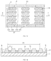
- FIG. 13 is a schematic top view of a sixth embodiment of an OLED substrate structure of the disclosure.
- FIG. 14 is a cross-sectional view corresponding to E-E in FIG. 13 .
- a first embodiment of an OLED substrate structure of the disclosure includes a base substrate 1 and a bank layer 3 disposed on the base substrate 1 .
- the bank layer 3 includes a plurality of accommodating grooves 31 arranged in array in a region corresponding to an effective display area AA of the OLED and a recess 33 arranged surrounding all the accommodating grooves 31 in a region corresponding to the periphery of the effective display area AA of the OLED.
- One of the accommodating grooves 31 corresponds to one pixel P, applied to accommodate an OLED organic functional layer D.
- the recess 33 has a rectangular frame shape with four sides communicated with each other.
- the recess 33 has a width of 0.1 mm to 50 mm; a distance between the recess 33 and a corresponding accommodating groove 31 located at the outermost edge of the effective display area AA of the OLED is 0.01 mm to 10 mm.
- the recess 33 is used for accommodating a solution containing the OLED organic functional layer material or a simple solvent; in this way, the pixel P corresponding to the edge of the effective display area of the OLED is close to the recess 33 instead of the air side, and the solution containing the OLED organic functional layer material or a simple solvent in the recess 33 also generates an atmosphere, so the atmosphere around the pixel P corresponding to the edge of the effective display area AA of the OLED is relatively uniform, thereby volatilizing the solvent uniformly to improve an uniformity of a film thickness of the OLED organic functional layer.
- FIGS. 5 and 6 are the second embodiment of the OLED substrate structure of the disclosure.
- the recess 33 includes a first recess 331 and a second recess 333 , and the first recess 331 and the second recess 333 are combined in a rectangular frame shape; and the first recess 331 occupies three communicating sides of the rectangular frame shape, and the second recess 333 occupies a remaining side of the rectangular frame shape.
- the remaining structures and the functions of the recess 33 are the same as those in the first embodiment, and will not be repeatedly described herein.
- FIGS. 7 and 8 are the third embodiment of the OLED substrate structure of the disclosure.
- the recess 33 includes a first recess 331 and a second recess 333 , and the first recess 331 and the second recess 333 are combined in a rectangular frame shape; and the first recess 331 occupies two communicating sides of the rectangular frame shape, and the second recess 333 occupies other two communicating sides of the rectangular frame shape.
- the remaining structures and the functions of the recess 33 are the same as those in the first embodiment, and will not be repeatedly described herein.
- FIGS. 9 and 10 is a fourth embodiment of the OLED substrate structure of the disclosure.
- the recess 33 includes a first recess 331 , a second recess 333 , and a third recess 335 , and the first recess 331 , the second recess 333 , and the third recess 335 are combined in a rectangular frame shape; the first recess 331 occupies two communicating sides of the rectangular frame shape, and the second recess 333 and the third recess 335 occupies other two communicating sides of the rectangular frame shape respectively.
- the remaining structures and the functions of the recess 33 are the same as those in the first embodiment, and will not be repeatedly described herein.
- FIGS. 11 and 12 are the fifth embodiment of the OLED substrate structure of the disclosure.
- the recess 33 includes the first recess 331 , the second recess 333 , the third recess 335 , and a fourth recess 337 , and the first recess 331 , the second recess 333 , the third recess 335 , and the fourth recess 337 are combined in a rectangular frame shape; and the first recess 331 , the second recess 333 , the third recess 335 , and the fourth recess 337 respectively occupy one of the sides of the rectangular frame shape.
- the remaining structures and the functions of the recess 33 are the same as those in the first embodiment, and will not be repeatedly described herein.
- FIGS. 13 and 14 are the sixth embodiment of the OLED substrate structure of the disclosure.
- the sixth embodiment is an improvement of the fifth embodiment, and the improvement is that each of the first recess 331 , the second recess 333 , the third recess 335 , and the fourth recess 337 includes at least two independent branch recesses B.
- the remaining structures and the functions of the recess 33 are the same as those in the fifth embodiment, and will not be repeatedly described herein.
- the above design of the OLED substrate structure can also be applied to a Quantum Dot Printed Display (QLED) substrate.
- QLED Quantum Dot Printed Display
- an OLED substrate structure by disposing a recess to contain a solution containing an OLED organic functional layer material or a simple solvent when the OLED device is fabricated by printing, ensures that the atmosphere around the pixels in each area is more uniform especially around the pixels at the edges of the effective display area of the OLED, thereby volatilizing the solvent uniformly to improve a uniformity of a film thickness of the OLED organic functional layer.
Abstract
Description
- The present application is a National Phase of International Application Number PCT/CN2017/113053, filed on Nov. 27, 2017, and claims the priority of China Application 201710963891.4, filed Oct. 16, 2017.
- The disclosure relates to the field of display technology, and in particular, to an OLED substrate structure.
- The organic light emitting diode (OLED) display apparatus is recognized by the industry as the most promising display device due to many advantages such as self-luminousness, low driving voltage, high luminous efficiency, short response time, high resolution and contrast, viewing angle nearly 180°, wide temperature range, and capability of achieving the flexible display and large-area panchromatic display.
- The OLED generally includes a substrate, an anode disposed on the substrate, a hole injection layer disposed on the anode, a hole transport layer disposed on the hole injection layer, and a light emitting layer disposed on the hole transport layer, an electron transport layer disposed on the light emitting layer, and a cathode disposed on the electron transport layer. The light-emitting principle of an OLED display device is that semiconductor materials and organic light-emitting materials emit light through carrier injection and recombination under an electric field. Specifically, an OLED display device generally adopts an ITO pixel electrode and a metal electrode as an anode and a cathode of the device respectively. Under a certain voltage, electrons and holes are injected from the cathode and the anode into the electron transport layer and the hole transport layer respectively. the electrons and holes migrate to the light emitting layer through the electron transport layer and the hole transport layer respectively, and meet in the light emitting layer to form excitons to excite the light-emitting molecules, which emit visible light through radiation relaxation.
- The fabricating methods of the existing OLED device are mainly divided into a vacuum thermal evaporation and a solution film-forming method, and the solution film-forming method is to firstly coat the solution containing the OLED organic functional layer material on the substrate, and then remove the solvent in the solution by a vacuum drying process, so that the solid substance in the solution forms a thin film on the substrate. Specifically, the solution film-forming method is subdivided into the methods such as spin coating, nozzle printing, and ink-jet printing method.
- Referring to
FIGS. 1 and 2 , a conventional OLED substrate includes abase substrate 100 and abank layer 300 disposed on thebase substrate 100. Thebank layer 300 includes a plurality ofaccommodating grooves 301 arranged in an array in the effective display area AA of the ° LED; one of theaccommodating grooves 301 corresponds to one pixel P, applied to accommodate an OLED organic functional layer. When the OLED device is fabricated by printing, theaccommodating groove 301 is used for accommodating the solution containing the OLED organic functional layer material, Since the atmosphere surrounding the pixel P at the edge of the effective display area AA is not uniform, the solvent on the side close to the air is volatilized quickly, thereby causing the solution in the pixel P to flow toward the air side for compensating, so that the film thickness of the OLED organic functional layer on the air side is thicker; and the atmosphere surrounding the pixel P in the middle of the effective display area AA is relatively uniform and the solvent is volatilized slowly and uniformly, and the thickness uniformity of the resulting OLED organic functional layer is better. - Since the uniformity of the film thickness distribution of the organic functional layer of the OLED directly affects the uniformity of light emission in the pixel P and the lifetime of the OLED device, it is necessary to improve the existing OLED substrate structure.
- The object of the disclosure is to provide an OLED substrate capable of making the ambient atmosphere around the pixels in each area uniform when the OLED device is fabricated by printing, and the solvent is volatilized uniformly to improve a uniformity of a film thickness of the OLED organic functional layer.
- In order to achieve the object, the disclosure provides an OLED substrate structure, including a base substrate and a bank layer disposed on the base substrate; and the bank layer includes a plurality of accommodating grooves arranged in array in a region corresponding to an effective display area of the OLED and a recess arranged surrounding all the accommodating grooves in a region corresponding to the periphery of the effective display area of the OLED;
- and one of the accommodating grooves corresponds to one pixel, applied to accommodate an OLED organic functional layer.
- Optionally, the recess is in a rectangular frame shape with four sides communicated with each other.
- Optionally, the recess includes a first recess and a second recess, and the first recess and the second recess are combined in a rectangular frame shape.
- The first recess occupies three communicating sides of the rectangular frame shape and the second recess occupies a remaining side of the rectangular frame shape.
- Or the first recess occupies two communicating sides of the rectangular frame shape, and the second recess occupies other two communicating sides of the rectangular frame shape.
- Optionally, the recess includes a first recess, a second recess and a third recess, and the first recess, the second recess, and the third recess are combined in a rectangular frame shape; the first recess occupies two communicating sides of the rectangular frame shape, and the second recess and the third recess occupy other two communicating sides of the rectangular frame shape respectively.
- Optionally, the recess includes a first recess, a second recess, a third recess, and a fourth recess; the first recess, the second recess, the third recess, and the fourth recess are combined in a rectangular frame shape; the first recess, the second recess, the third recess, and the fourth recess respectively occupy one of the sides of the rectangular frame shape.
- Further, each of the first recess, the second recess, the third recess, and the fourth recess includes at least two independent branch recesses.
- The recess has a width of 0.1 mm to 50 mm.
- A distance between the recess and a corresponding accommodating groove located at the outermost edge of the effective display area of the OLED is 0.01 mm to 10 mm.
- The disclosure further provides an OLED substrate structure including a base substrate and a bank layer disposed on the base substrate; and the bank layer includes a plurality of accommodating grooves arranged in array in a region corresponding to an effective display area of the OLED and a recess arranged surrounding all the accommodating grooves in a region corresponding to the periphery of the effective display area of the OLED;
- one of the accommodating grooves corresponds to one pixel, applied to accommodate an OLED organic functional layer;
- the recess includes a first recess; a second recess; a third recess, and a fourth recess; the first recess, the second recess, the third recess, and the fourth recess are combined in the rectangular frame shape. Each of the first recess, the second recess, the third recess, and the fourth recess occupies one of the sides of the rectangular frame shape; and
- each of the first recess, the second recess, the third recess, and the fourth recess includes at least two independent branch recesses;
- the recess has a width of 0.1 mm to 50 mm; and
- a distance between the recess and a corresponding accommodating groove located at the outermost edge of the effective display area of the OLED is 0.01 mm to 10 mm.
- The beneficial effect of the disclosure is that the disclosure provides an OLED substrate structure; by disposing a recess to contain a solution containing an OLED organic functional layer material or a simple solvent when the OLED device is fabricated by printing, ensures that the atmosphere around the pixels in each area is more uniform in particular around the pixels at the edges of the effective display area of the OLED, thereby volatilizing the solvent uniformly to improve an uniformity of a film thickness of the OLED organic functional layer.
- For further understanding of the features and technical contents of the disclosure, reference should be made to the following detailed description and accompanying drawings of the disclosure. However, the drawings are for reference only and are not intended to limit the disclosure.
- In the drawings,
-
FIG. 1 is a cross-sectional view of a conventional OLED substrate structure in a process of fabricating an OLED device by printing; -
FIG. 2 is a schematic top view of the conventional OLED substrate structure; -
FIG. 3 is a schematic top view of a first embodiment of an OLED substrate structure of the disclosure; -
FIG. 4 is a cross-sectional view corresponding to E-E inFIG. 3 ; -
FIG. 5 is a schematic top view of a second embodiment of the OLED substrate structure of the disclosure; -
FIG. 6 is a cross-sectional view corresponding to E-E inFIG. 5 ; -
FIG. 7 is a schematic top view of a third embodiment of the OLED substrate structure of the disclosure; -
FIG. 8 is a cross-sectional view corresponding to E-E inFIG. 7 ; -
FIG. 9 is a schematic top view of a fourth embodiment of the OLED substrate structure of the disclosure; -
FIG. 10 is a cross-sectional view corresponding to E-E inFIG. 9 ; -
FIG. 11 is a schematic top view of a fifth embodiment of the OLED substrate structure of the disclosure; -
FIG. 12 is a cross-sectional view corresponding to E-E inFIG. 11 ; -
FIG. 13 is a schematic top view of a sixth embodiment of an OLED substrate structure of the disclosure; and -
FIG. 14 is a cross-sectional view corresponding to E-E inFIG. 13 . - To further illustrate the technical means adopted by the disclosure and the effects thereof, the following describes in detail the preferred embodiments of the disclosure and the accompanying drawings.
- The disclosure provides an OLED substrate structure. Please refer to
FIGS. 3 and 4 together, a first embodiment of an OLED substrate structure of the disclosure includes abase substrate 1 and a bank layer 3 disposed on thebase substrate 1. The bank layer 3 includes a plurality ofaccommodating grooves 31 arranged in array in a region corresponding to an effective display area AA of the OLED and arecess 33 arranged surrounding all theaccommodating grooves 31 in a region corresponding to the periphery of the effective display area AA of the OLED. One of theaccommodating grooves 31 corresponds to one pixel P, applied to accommodate an OLED organic functional layer D. - As shown in
FIGS. 3 and 4 , in the first embodiment; therecess 33 has a rectangular frame shape with four sides communicated with each other. - Specifically, the
recess 33 has a width of 0.1 mm to 50 mm; a distance between therecess 33 and acorresponding accommodating groove 31 located at the outermost edge of the effective display area AA of the OLED is 0.01 mm to 10 mm. - When the OLED device is fabricated by printing, the
recess 33 is used for accommodating a solution containing the OLED organic functional layer material or a simple solvent; in this way, the pixel P corresponding to the edge of the effective display area of the OLED is close to therecess 33 instead of the air side, and the solution containing the OLED organic functional layer material or a simple solvent in therecess 33 also generates an atmosphere, so the atmosphere around the pixel P corresponding to the edge of the effective display area AA of the OLED is relatively uniform, thereby volatilizing the solvent uniformly to improve an uniformity of a film thickness of the OLED organic functional layer. - Please refer to
FIGS. 5 and 6 together, which are the second embodiment of the OLED substrate structure of the disclosure. The difference between the second embodiment and the first embodiment in that therecess 33 includes afirst recess 331 and asecond recess 333, and thefirst recess 331 and thesecond recess 333 are combined in a rectangular frame shape; and thefirst recess 331 occupies three communicating sides of the rectangular frame shape, and thesecond recess 333 occupies a remaining side of the rectangular frame shape. The remaining structures and the functions of therecess 33 are the same as those in the first embodiment, and will not be repeatedly described herein. - Please refer to
FIGS. 7 and 8 together, which are the third embodiment of the OLED substrate structure of the disclosure. The difference between the third embodiment and the first embodiment is that therecess 33 includes afirst recess 331 and asecond recess 333, and thefirst recess 331 and thesecond recess 333 are combined in a rectangular frame shape; and thefirst recess 331 occupies two communicating sides of the rectangular frame shape, and thesecond recess 333 occupies other two communicating sides of the rectangular frame shape. The remaining structures and the functions of therecess 33 are the same as those in the first embodiment, and will not be repeatedly described herein. - Please refer to
FIGS. 9 and 10 together, which is a fourth embodiment of the OLED substrate structure of the disclosure. The difference between the fourth embodiment and the first embodiment in that therecess 33 includes afirst recess 331, asecond recess 333, and athird recess 335, and thefirst recess 331, thesecond recess 333, and thethird recess 335 are combined in a rectangular frame shape; thefirst recess 331 occupies two communicating sides of the rectangular frame shape, and thesecond recess 333 and thethird recess 335 occupies other two communicating sides of the rectangular frame shape respectively. The remaining structures and the functions of therecess 33 are the same as those in the first embodiment, and will not be repeatedly described herein. - Please refer to
FIGS. 11 and 12 together, which are the fifth embodiment of the OLED substrate structure of the disclosure. The difference between the fifth embodiment and the first embodiment in that therecess 33 includes thefirst recess 331, thesecond recess 333, thethird recess 335, and afourth recess 337, and thefirst recess 331, thesecond recess 333, thethird recess 335, and thefourth recess 337 are combined in a rectangular frame shape; and thefirst recess 331, thesecond recess 333, thethird recess 335, and thefourth recess 337 respectively occupy one of the sides of the rectangular frame shape. The remaining structures and the functions of therecess 33 are the same as those in the first embodiment, and will not be repeatedly described herein. - Please refer to
FIGS. 13 and 14 , which are the sixth embodiment of the OLED substrate structure of the disclosure. The sixth embodiment is an improvement of the fifth embodiment, and the improvement is that each of thefirst recess 331, thesecond recess 333, thethird recess 335, and thefourth recess 337 includes at least two independent branch recesses B. The remaining structures and the functions of therecess 33 are the same as those in the fifth embodiment, and will not be repeatedly described herein. - The above design of the OLED substrate structure can also be applied to a Quantum Dot Printed Display (QLED) substrate.
- To sum up, an OLED substrate structure, by disposing a recess to contain a solution containing an OLED organic functional layer material or a simple solvent when the OLED device is fabricated by printing, ensures that the atmosphere around the pixels in each area is more uniform especially around the pixels at the edges of the effective display area of the OLED, thereby volatilizing the solvent uniformly to improve a uniformity of a film thickness of the OLED organic functional layer.
- In view of the above, those skilled in the art can make various other corresponding changes and modifications according to the technical solutions and technical solutions of the disclosure, and all such changes and modifications shall fall within the protection scope of the claims of the disclosure range.
Claims (11)
Applications Claiming Priority (3)
| Application Number | Priority Date | Filing Date | Title |
|---|---|---|---|
| CN201710963891.4 | 2017-10-16 | ||
| CN201710963891.4A CN107732026A (en) | 2017-10-16 | 2017-10-16 | OLED substrate structure |
| PCT/CN2017/113053 WO2019075855A1 (en) | 2017-10-16 | 2017-11-27 | Oled substrate structure |
Publications (1)
| Publication Number | Publication Date |
|---|---|
| US20200052062A1 true US20200052062A1 (en) | 2020-02-13 |
Family
ID=61211361
Family Applications (1)
| Application Number | Title | Priority Date | Filing Date |
|---|---|---|---|
| US15/736,506 Abandoned US20200052062A1 (en) | 2017-10-16 | 2017-11-27 | Oled substrate structure |
Country Status (3)
| Country | Link |
|---|---|
| US (1) | US20200052062A1 (en) |
| CN (1) | CN107732026A (en) |
| WO (1) | WO2019075855A1 (en) |
Cited By (1)
| Publication number | Priority date | Publication date | Assignee | Title |
|---|---|---|---|---|
| US20220208892A1 (en) * | 2020-12-28 | 2022-06-30 | Samsung Display Co., Ltd. | Manufacturing method of display device and display device using the same |
Families Citing this family (2)
| Publication number | Priority date | Publication date | Assignee | Title |
|---|---|---|---|---|
| CN108281474B (en) | 2018-03-28 | 2019-05-10 | 京东方科技集团股份有限公司 | Organic light emitting display panel and preparation method thereof, display device |
| CN110544713B (en) * | 2019-09-09 | 2022-08-26 | 合肥京东方卓印科技有限公司 | Display panel and manufacturing method thereof |
Citations (1)
| Publication number | Priority date | Publication date | Assignee | Title |
|---|---|---|---|---|
| US20140161968A1 (en) * | 2012-12-10 | 2014-06-12 | Samsung Display Co., Ltd. | Inkjet printhead and apparatus and method for manufacturing organic luminescence display using the inkjet printhead |
Family Cites Families (5)
| Publication number | Priority date | Publication date | Assignee | Title |
|---|---|---|---|---|
| JP2000091083A (en) * | 1998-09-09 | 2000-03-31 | Sony Corp | Organic el display |
| CN1921136B (en) * | 2000-11-27 | 2012-05-09 | 精工爱普生株式会社 | Organic electroluminescent device, and manufacture method thereof |
| JP2010104861A (en) * | 2008-10-28 | 2010-05-13 | Seiko Epson Corp | Method of ejecting liquid material, method of manufacturing color filter and method of manufacturing organic el device |
| CN102226998A (en) * | 2011-06-15 | 2011-10-26 | 友达光电股份有限公司 | Organic light-emitting pixel array |
| CN104409471B (en) * | 2014-11-04 | 2018-07-24 | 京东方科技集团股份有限公司 | A kind of display base plate and its application method, polymer electroluminescent device |
-
2017
- 2017-10-16 CN CN201710963891.4A patent/CN107732026A/en active Pending
- 2017-11-27 US US15/736,506 patent/US20200052062A1/en not_active Abandoned
- 2017-11-27 WO PCT/CN2017/113053 patent/WO2019075855A1/en active Application Filing
Patent Citations (1)
| Publication number | Priority date | Publication date | Assignee | Title |
|---|---|---|---|---|
| US20140161968A1 (en) * | 2012-12-10 | 2014-06-12 | Samsung Display Co., Ltd. | Inkjet printhead and apparatus and method for manufacturing organic luminescence display using the inkjet printhead |
Cited By (1)
| Publication number | Priority date | Publication date | Assignee | Title |
|---|---|---|---|---|
| US20220208892A1 (en) * | 2020-12-28 | 2022-06-30 | Samsung Display Co., Ltd. | Manufacturing method of display device and display device using the same |
Also Published As
| Publication number | Publication date |
|---|---|
| CN107732026A (en) | 2018-02-23 |
| WO2019075855A1 (en) | 2019-04-25 |
Similar Documents
| Publication | Publication Date | Title |
|---|---|---|
| KR102322637B1 (en) | Exclusive liquid OLED device and its manufacturing method | |
| US10784471B2 (en) | Organic light emitting display device and method of making the same | |
| US11171188B2 (en) | Organic light-emitting diode device, organic light-emitting diode display apparatus, and preparation method for organic light-emitting diode device | |
| US10510990B2 (en) | Groove structure for printing OLED display and manufacturing method for OLED display | |
| US9954170B2 (en) | Recess structure for print deposition process and manufacturing method thereof | |
| US10084132B2 (en) | Groove structure for printing coating process and manufacturing method thereof | |
| CN107623021B (en) | OLED display manufacturing method and OLED display | |
| US10781326B2 (en) | Ink-jet printing ink of an electron transport layer and its manufacturing method | |
| US20210359259A1 (en) | Display panel and display device | |
| US10305049B2 (en) | OLED substrate and manufacture method thereof | |
| US20140084258A1 (en) | Organic light emitting display device | |
| KR20070106240A (en) | Organic electro luminescence device and method of manufacturing the same | |
| US20200052062A1 (en) | Oled substrate structure | |
| KR20140045157A (en) | Organic light emitting display and method of manufacturing the same | |
| CN107978691B (en) | Organic light-emitting display panel, display device and manufacturing method of display panel | |
| WO2019041578A1 (en) | Oled substrate and manufacturing method therefor | |
| KR20190071795A (en) | OLED substrate and manufacturing method thereof | |
| US20140041586A1 (en) | Masking Device for Vapor Deposition of Organic Material of Organic Electroluminescent Diode | |
| US20190067389A1 (en) | Oled substrate and fabrication method thereof | |
| US11716866B2 (en) | Display panel including planarization layer with protrusion and method of manufacturing thereof | |
| KR101296651B1 (en) | Method of manufacturing Organic Electroluminescent Device | |
| CN108520891B (en) | Ink-jet printing method of array substrate, array substrate and display device | |
| US20210119176A1 (en) | Oled encapsulation method and oled encapsulation structure | |
| US20180240999A1 (en) | Oled encapsulation method and oled encapsulation structure | |
| CN110085652B (en) | OLED substrate |
Legal Events
| Date | Code | Title | Description |
|---|---|---|---|
| AS | Assignment |
Owner name: SHENZHEN CHINA STAR OPTOELECTRONICS SEMICONDUCTOR DISPLAY TECHNOLOGY CO., LTD., CHINA Free format text: ASSIGNMENT OF ASSIGNORS INTEREST;ASSIGNORS:LIU, YAWEI;WU, TSUNGYUAN;REEL/FRAME:044398/0535 Effective date: 20171129 |
|
| STPP | Information on status: patent application and granting procedure in general |
Free format text: NON FINAL ACTION MAILED |
|
| STPP | Information on status: patent application and granting procedure in general |
Free format text: RESPONSE TO NON-FINAL OFFICE ACTION ENTERED AND FORWARDED TO EXAMINER |
|
| STPP | Information on status: patent application and granting procedure in general |
Free format text: FINAL REJECTION MAILED |
|
| STCB | Information on status: application discontinuation |
Free format text: ABANDONED -- FAILURE TO RESPOND TO AN OFFICE ACTION |