US20190131663A1 - Battery pack protection circuit module - Google Patents
Battery pack protection circuit module Download PDFInfo
- Publication number
- US20190131663A1 US20190131663A1 US16/142,885 US201816142885A US2019131663A1 US 20190131663 A1 US20190131663 A1 US 20190131663A1 US 201816142885 A US201816142885 A US 201816142885A US 2019131663 A1 US2019131663 A1 US 2019131663A1
- Authority
- US
- United States
- Prior art keywords
- pcb
- face
- battery
- pair
- electrodes
- Prior art date
- Legal status (The legal status is an assumption and is not a legal conclusion. Google has not performed a legal analysis and makes no representation as to the accuracy of the status listed.)
- Granted
Links
Images


Classifications
-
- H—ELECTRICITY
- H01—ELECTRIC ELEMENTS
- H01M—PROCESSES OR MEANS, e.g. BATTERIES, FOR THE DIRECT CONVERSION OF CHEMICAL ENERGY INTO ELECTRICAL ENERGY
- H01M10/00—Secondary cells; Manufacture thereof
- H01M10/42—Methods or arrangements for servicing or maintenance of secondary cells or secondary half-cells
- H01M10/425—Structural combination with electronic components, e.g. electronic circuits integrated to the outside of the casing
-
- H—ELECTRICITY
- H01—ELECTRIC ELEMENTS
- H01M—PROCESSES OR MEANS, e.g. BATTERIES, FOR THE DIRECT CONVERSION OF CHEMICAL ENERGY INTO ELECTRICAL ENERGY
- H01M50/00—Constructional details or processes of manufacture of the non-active parts of electrochemical cells other than fuel cells, e.g. hybrid cells
- H01M50/50—Current conducting connections for cells or batteries
- H01M50/543—Terminals
- H01M50/547—Terminals characterised by the disposition of the terminals on the cells
- H01M50/55—Terminals characterised by the disposition of the terminals on the cells on the same side of the cell
-
- H—ELECTRICITY
- H01—ELECTRIC ELEMENTS
- H01M—PROCESSES OR MEANS, e.g. BATTERIES, FOR THE DIRECT CONVERSION OF CHEMICAL ENERGY INTO ELECTRICAL ENERGY
- H01M50/00—Constructional details or processes of manufacture of the non-active parts of electrochemical cells other than fuel cells, e.g. hybrid cells
- H01M50/50—Current conducting connections for cells or batteries
- H01M50/543—Terminals
- H01M50/552—Terminals characterised by their shape
- H01M50/553—Terminals adapted for prismatic, pouch or rectangular cells
-
- H—ELECTRICITY
- H05—ELECTRIC TECHNIQUES NOT OTHERWISE PROVIDED FOR
- H05K—PRINTED CIRCUITS; CASINGS OR CONSTRUCTIONAL DETAILS OF ELECTRIC APPARATUS; MANUFACTURE OF ASSEMBLAGES OF ELECTRICAL COMPONENTS
- H05K1/00—Printed circuits
- H05K1/18—Printed circuits structurally associated with non-printed electric components
- H05K1/181—Printed circuits structurally associated with non-printed electric components associated with surface mounted components
-
- H—ELECTRICITY
- H05—ELECTRIC TECHNIQUES NOT OTHERWISE PROVIDED FOR
- H05K—PRINTED CIRCUITS; CASINGS OR CONSTRUCTIONAL DETAILS OF ELECTRIC APPARATUS; MANUFACTURE OF ASSEMBLAGES OF ELECTRICAL COMPONENTS
- H05K3/00—Apparatus or processes for manufacturing printed circuits
- H05K3/30—Assembling printed circuits with electric components, e.g. with resistors
- H05K3/32—Assembling printed circuits with electric components, e.g. with resistors electrically connecting electric components or wires to printed circuits
-
- H—ELECTRICITY
- H01—ELECTRIC ELEMENTS
- H01M—PROCESSES OR MEANS, e.g. BATTERIES, FOR THE DIRECT CONVERSION OF CHEMICAL ENERGY INTO ELECTRICAL ENERGY
- H01M10/00—Secondary cells; Manufacture thereof
- H01M10/42—Methods or arrangements for servicing or maintenance of secondary cells or secondary half-cells
- H01M10/425—Structural combination with electronic components, e.g. electronic circuits integrated to the outside of the casing
- H01M2010/4271—Battery management systems including electronic circuits, e.g. control of current or voltage to keep battery in healthy state, cell balancing
-
- H—ELECTRICITY
- H05—ELECTRIC TECHNIQUES NOT OTHERWISE PROVIDED FOR
- H05K—PRINTED CIRCUITS; CASINGS OR CONSTRUCTIONAL DETAILS OF ELECTRIC APPARATUS; MANUFACTURE OF ASSEMBLAGES OF ELECTRICAL COMPONENTS
- H05K2201/00—Indexing scheme relating to printed circuits covered by H05K1/00
- H05K2201/10—Details of components or other objects attached to or integrated in a printed circuit board
- H05K2201/10007—Types of components
- H05K2201/10037—Printed or non-printed battery
-
- Y—GENERAL TAGGING OF NEW TECHNOLOGICAL DEVELOPMENTS; GENERAL TAGGING OF CROSS-SECTIONAL TECHNOLOGIES SPANNING OVER SEVERAL SECTIONS OF THE IPC; TECHNICAL SUBJECTS COVERED BY FORMER USPC CROSS-REFERENCE ART COLLECTIONS [XRACs] AND DIGESTS
- Y02—TECHNOLOGIES OR APPLICATIONS FOR MITIGATION OR ADAPTATION AGAINST CLIMATE CHANGE
- Y02E—REDUCTION OF GREENHOUSE GAS [GHG] EMISSIONS, RELATED TO ENERGY GENERATION, TRANSMISSION OR DISTRIBUTION
- Y02E60/00—Enabling technologies; Technologies with a potential or indirect contribution to GHG emissions mitigation
- Y02E60/10—Energy storage using batteries
Definitions
- a common mechanism for providing battery power to portable electronic devices is by use of modular secondary battery packs.
- battery packs often employ rechargeable lithium-ion based battery cells, such as lithium-ion polymer battery cells, also known as Li-Poly, Li-Pol, or LiPo cells.
- a protection circuit module is usually included in the battery pack, being connected to the battery cell by a pair of electrodes to perform protective functions with respect to operation of the battery cell.
- Typical functions of the PCM include preventing overcharge, preventing over discharge, and preventing over-current of the battery cell.
- FIGS. 1A and 1B shows a battery pack according to existing structural arrangements.
- FIG. 1A is a schematic three-dimensional view of an existing battery pack, in which a PCM insulation cover is removed for clarity of view.
- FIG. 1B is a partial cross-section, on an enlarged scale, of the existing battery pack of FIG. 1A .
- FIG. 2A is a partially exposed schematic three-dimensional view of a battery pack according to one example embodiment, a PCM insulation cover being omitted for clarity of illustration.
- FIG. 2B is a partial cross-section, on an enlarged scale, of the example battery pack of FIG. 2A .
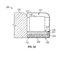
- FIG. 3A is a schematic partial cross-section of a battery pack according to another example embodiment, in which electrode terminals are provided on an edge face of a protective circuit board (PCB) of the PCM.
- PCB protective circuit board
- FIG. 3B is a schematic three-dimensional view, on a reduced scale, of a battery pack according to the example embodiment of FIG. 3A .
- FIG. 4A is a partial cross-sectional view of a battery pack according to an example embodiment in which a pair of PCMs for a corresponding pair of battery cells share a common PCB.
- FIG. 4B is a view corresponding to FIG. 4A , showing an intermediate stage during manufacture of a battery pack according to the example embodiment of FIG. 4A .
- FIG. 5B is a partial cross-sectional view of a battery pack according to an example embodiment in which a pair of PCMs for a corresponding pair of battery cells share an edge-mounted PCB in common.
- FIG. 5A is a view corresponding to FIG. 5B , showing an intermediate stage during manufacturing of a battery pack according to the example embodiment of FIG. 5B .
- FIGS. 1A and 1B show an example of an existing battery pack structure.
- the conventional battery pack 100 of FIG. 1A includes a lithium polymer battery cell 103 coupled to a safety circuit in the form of a protection circuit module (PCM) 112 .
- the PCM 112 provides power control functionality to the battery cell 103 , e.g. for safety purposes.
- the PCM prevents overcharge, over-discharge, and/or overcurrent in the battery cell 103 .
- the PCM 112 is connected to the battery cell 103 by a pair of electrodes 109 that project from the battery cell 103 .
- the pair of electrodes 109 are terminals of the battery cell 103 , consisting of a cathode and an anode.
- the PCM 112 comprises a printed circuit board or protection circuit board (PCB) 115 and a plurality of PCM components mounted on the PCB 115 , the available volume for location of PCM components on the PCB 115 being indicated in the drawings by PCM block 118 .
- the PCB 115 comprises a rectangular substrate carrying an integrated protection circuit thereon for connection to the PCM components and to the battery electrodes 109 .
- the assembly consisting of the battery cell 103 and the PCM 112 is housed in a casing 106 , part of which provides insulation 131 covering for the PCM 112 .
- the insulation 131 and its analogs are consistently omitted from schematic three-dimensional views of respective embodiments, such as in the FIGS. 1A, 2A, and 3B .
- the PCB 115 has a pair of substantially rectangular major outer surfaces which are substantially parallel to one another and which face in opposite outward directions.
- these opposite major faces are designated as a top face 124 and a bottom face 125 .
- reference to the top and bottom faces do not indicate a particular orientation or spatial attribute of the respective faces, but is instead used as monikers to distinguish between these two faces in description.
- that face of the PCB 115 on which all or the majority of contacts or nodes of the integrated protective circuit are available for connection of PCM components is, unless the context clearly indicates otherwise, referred to as the top face 124 .
- the top and bottom faces 124 , 125 are connected by a peripheral edge face that extends transversely between them.
- the edge face includes a pair of end edge faces at the longitudinal end edges of the PCB 115 , and a pair of side edge faces 135 , 136 at the lateral side edges of the PCB 115 .
- the side edge faces (best seen in FIG. 1B ) are designated as a front edge face 135 furthest from the battery cell 103 , and a rear edge face 136 closest to the battery cell 103 .
- the PCB 115 is oriented such that a widthwise dimension of the PCB 115 (i.e., the dimension extending between the side edge faces 135 , 136 ) is substantially parallel to the lengthwise direction of the battery cell 103 .
- a lengthwise direction of the PCB 115 i.e., the dimension of the PCB 115 that extends between its end edges
- the thickness dimension of the PCB 115 is oriented transversely to the lengthwise direction of the battery cell 103 .
- connections of the respective electrodes 109 to the PCB 115 are in the existing battery back 100 located on the top face 124 of the PCB 115 .
- Respective metal tabs e.g., copper tabs
- the electrodes 109 project longitudinally (relatively to the lengthwise direction of the battery cell 103 ) from the battery cell 103 , pass beneath the bottom face 125 of the PCB 115 , and are bent 180° to fold over into contact with the top face 124 .
- the electrodes 109 are typically soldered to respective metal terminal pads provided on the PCB 115 .
- the metal terminal pads are gold-plated surfaces forming part of the protection circuit carried by the PCB 115 .
- One aspect of the disclosure provides for locating electrode connections of a battery cell to a PCM's PCB on a face of the PCB other than a major face that receives PCM components thereon. Such separation of electrode connections from the major face of the PCB on which PCM components are mounted makes available for the mounting of PCM components substantially the entirety of the PCM-hosting major face of the PCB.
- electrode connections to the PCB may be provided on its edge face, or on a bottom face opposite the top face on which the PCM components are mounted.
- enlarged terminal pads e.g. being widened relative to a main connective portion of the electrode projecting from the battery cell
- copper plated surfaces may be provided on the edge face of the PCB, for example by copper plated surfaces.
- the PCB may have an orientation in which its thickness dimension is substantially parallel to the lengthwise direction of the battery cell (thus having an orientation rotated more or less than 90° relative to the position of the PCB 115 shown in FIG. 1B ).
- the battery pack may comprise a pair of battery cells flanking the PCB, with both of the battery cells being connected to the PCB such that respective PCM modules of the two battery cells share a single PCB in common.
- FIGS. 2-5 A number of specific example embodiments will now be described in greater detail with reference to the FIGS. 2-5 .
- the same reference numerals are used for indicating corresponding parts or elements in FIG. 1 and in FIGS. 2-5 , even when there are in some instances differences between the specifics of the corresponding parts or elements.
- FIGS. 2A and 2B show an example battery pack 200 in which the electrodes 109 are conductively coupled to the PCB 115 on its bottom face 125 . This is in contradistinction to the conventional coupling of the electrodes 109 to the top face 124 of the PCB 115 , as discussed with reference to FIG. 1 .
- a further difference between the prior battery pack construction of FIG. 1 and the example embodiment of FIG. 2 is that the PCB 115 has a different orientation, in that its widthwise dimension is oriented transversely relative to the lengthwise direction of the battery cell 103 . This can best be seen in the sectional side view of FIG.
- the upright orientation of the PCB 115 is such that the top face 124 faces towards the battery cell 103 , the bottom face 125 facing away from the battery cell 103 .
- the PCM block 118 with its various components are located on the top face 124 , thus being sandwiched between the PCB 115 and battery cell 103 .
- the electrodes 109 project longitudinally from the battery cell 103 , extending past the PCM block 118 and the PCB 115 , being bent through about 90° to lie flat against and in contact with the bottom face 125 of the PCB 115 .
- the bottom face of the PCB 115 provides respective conductive terminal pads to which the electrodes 109 are connected, the terminal pads being coupled to the integrated protection circuit of the PCB 115 to provide an electronic connection between the electrodes 109 and the PCM components forming part of the PCM block 118 .
- the terminal pads on the bottom face 125 are gold-plated surfaces to which the respective electrodes are soldered.
- Such a reduction in maximal dimensions of the PCM block 118 can in turn be utilized to achieve a reduction in the maximal dimensions of the PCM module 112 as a whole, allowing for a smaller battery pack 200 with similar performance attributes, or allowing for the battery pack 200 to have a larger, greater capacity battery cell 103 for a constant battery pack size.
- FIGS. 3A and 3B shows another example battery pack 300 that provides for a PCM component-receiving top face 124 that is uninterrupted by any electrode connections thereon.
- the electrodes 109 are connected to the edge face of the PCB 115 , in particular being connected to the front edge face 135 .
- the orientation of the PCB 115 in the battery pack 300 is similar to that which is the case in the previously described existing battery pack 100 ( FIG. 1B ), in that the thickness dimension of the PCB 115 (i.e., the direction extending between the top face 124 and the bottom face 125 ) is oriented transversely to the lengthwise direction of the battery cell 103 .
- a main, connective electrode portion provided by an electrode 309 projects longitudinally from the battery cell 103 , passes beneath the bottom face 125 of the PCB 115 , and is bent substantially 90° such that terminal end portions 317 of the respective electrodes 109 lie flat against the PCB's front edge face 135 , which is directed longitudinally away from the battery cell 103 .
- connection pads 324 are provided by gold-plated surfaces on the front edge face 135 , connection of the electrodes 109 thereto being achieved by solder joint attachment of the terminal end portions 317 to the respective connection pads 324 .
- the electrodes 109 can be welded to the exposed gold pads 324 .
- the connection pads 324 are conductively coupled to the integrated circuit of the PCB 115 .
- the increased width of the terminal end portions 317 and connection pads 324 are selected such that the contact surface between the terminal end portions 317 and the connection pads 324 are at least as great as the corresponding contact surface between the conventionally structured electrodes 109 and the PCB 115 of existing battery packs, such as the battery pack 100 described with reference to FIG. 1 .
- top face 124 makes substantially the entire flat surface of the top face 124 available to place PCM components.
- the additional free area on the top face 124 can be optimized for allowing a more compact PCB 115 .
- a PCB 115 that has a smaller width i.e., a smaller spacing between the front and rear side edges 135 , 136
- offers comparable PCM block volume that is the case with the existing battery pack 100 of FIG. 1 .
- space saving can translate to a shorter battery pack 300 for a given battery capacity, or can be used to increase battery capacity for a given battery pack size.
- arrangement of battery electrode connections to a PCM's PCB such that substantially an entire major outer face of the PCB is available for PCM component attachment is combined with a PCM nesting arrangement in which two separate battery cells or units share a common PCM, having a single PCB.
- FIG. 4A One example embodiment of such an arrangement is illustrated schematically in FIG. 4A .
- the orientation of the PCB 115 and the connection thereof to a first battery cell 103 . 1 corresponds to the arrangement illustrated and discussed with reference to FIGS. 2A and 2B .
- the PCB 115 thus has an upright orientation in which its widthwise direction is transverse to the lengthwise direction of the first battery cell 103 . 1 , the thickness dimension of the PCB 115 being parallel to the lengthwise direction of the battery cell 103 . 1 .
- the electrodes 109 . 1 of the first battery cell 103 . 1 are connected to the bottom face 125 of the battery cell 103 , leaving a primary PCM block 118 . 1 on the top face 124 of the PCB 115 unimpeded by the electrodes 109 . 1 .
- the top face 124 is opposed to and directed towards the battery cell 103 . 1 .
- the battery pack 400 includes a second, additional battery cell 103 . 2 which is substantially identical to the first battery cell 103 . 1 .
- the second battery cell 103 . 2 is longitudinally aligned with the first battery cell 103 . 1 , being arranged end-to-end with the first battery cell 103 . 1 with a longitudinal spacing between them, within which a common PCM 112 is housed for serving both battery cells 103 . 1 , 103 . 2 .
- the two battery cells of the battery pack 400 lie substantially in a common plane.
- the electrodes 109 . 2 of the second battery cell 103 . 2 are conductively coupled to the PCB 115 on the same face as the connection of the electrodes 109 . 1 of the first battery cell 103 . 1 , in this example embodiment being connected to the bottom face 125 of the PCB 115 .
- the second battery cell 103 . 2 is inverted relative to the first battery cell 103 . 1 , such that the electrodes 109 . 1 , 109 . 2 of the respective battery cells extend toward opposite side edges of the PCB 115 .
- the respective electrodes 109 of the pair of battery cells 103 are connected together at their common connection to the bottom face 125 of the PCB 115 .
- the first battery electrodes 109 are conductively coupled to the PCB 115 on the same face as the connection of the electrodes 109 . 1 of the first battery cell 103 . 1 , in this example embodiment being connected to the bottom face 125 of the PCB 115 .
- connection pads 109 . 1 are soldered or welded to respective exposed copper connection pads on the bottom face 125 , substantially covering the connection pads.
- the second battery electrodes 109 . 2 are in turn soldered or welded to the exposed rear surfaces of the first electrodes 109 . 1 .
- separate connection surfaces or pads may be provided on the bottom face 125 for all four electrodes 109 . 1 , 109 . 2 .
- the second electrodes 109 . 2 are not attached to the first electrodes 109 . 1 , but are instead soldered or welded directly to the PCB 115 at the bottom face 125 .
- the top face 124 of the PCB 115 is uninterrupted by any electrode connections, and is substantially entirely available for the attachment of PCM components in a primary PCM block 118 . 1 .
- Additional PCM components are placed in a secondary PCM block 118 . 2 on those parts of the bottom face 125 that are not reserved for the electrode connections.
- the secondary PCM block 118 . 2 thus has three interrupted sub-blocks, being similar in arrangement and appearance to the PCM sub-blocks 118 ′, 118 ′′, and 118 ′′′ of FIG. 1A .
- FIG. 4B shows the spatial arrangement of different components of the battery pack 400 during an intermediate step of manufacturing the finalized battery pack 400 of FIG. 4A .
- respective electrode tabs in a rectilinear, unbent state are soldered or welded to the bottom face 125 of the PCB 115 while the PCB 115 is oriented such that its widthwise direction is aligned with the lengthwise directions of the battery cells 103 . 1 , 103 . 2 .
- Such a process results in the arrangement seen in FIG. 4B .
- the PCM 112 (comprising the single, common PCB 115 , the primary PCM block 118 8 . 1 , and the second of the PCM block 118 . 2 ) is rotated through approximately 90° into its position shown in FIG. 4A .
- the respective electrode tabs 109 . 1 , 109 . 2 are bent or folded to assume the shapes shown in FIG. 4A .
- the described method of assembly of the battery pack 400 described with reference to the FIG. 4B has the benefit of providing greater accessibility to the PCB 115 during electrode attachment than would have been the case if the respective components were to be connected in the final position of FIG. 4 .
- FIG. 5B shows a further example embodiment of a dual-cell battery pack 500 in a nested arrangement in which two battery cells 103 . 1 , 103 . 2 share a single PCM 112 in common, with a single PCB 115 serving both battery cells of the battery pack 500 .
- the battery pack 500 of FIG. 5 is thus similar in arrangement to the battery pack 400 of FIG. 4 , with a major distinction being that the electrode connections are provided on the edge face of the PCB 115 , rather than on the bottom face 125 as is the case in FIG. 4 .
- each of the respective pair of battery electrodes 109 . 1 , 109 . 2 is connected (in a manner substantially identical to that described with reference to FIGS. 3A and 3B ) to a respective side edge face 135 , 136 of the PCB 115 .
- each side edge face of the PCB 115 is provided with a pair of widened copper terminal connection pads 324 connected to the integrated protection circuit of the PCB 115 .
- Each of the four electrode tabs similarly has a respective widened end portion 317 that is connected to a respective one of the edge-mounted connection pads 324 . 1 , 324 . 2 by soldering or welding.
- FIG. 5A shows an intermediate step in the manufacturing of the finalized battery pack 500 of FIG. 5B .
- the respective end portions 317 . 1 , 317 . 2 of the electrodes 109 . 1 , 109 . 2 are soldered to the corresponding edge-mounted contact pads 324 . 1 , 324 . 2 while the electrodes 109 . 1 , 109 . 2 are rectilinear and extend in the directions indicated by dotted lines 520 in FIG. 5A .
- the PCB 115 is oriented relative to the battery cells 103 , 103 ′ such that its widthwise dimension is transverse to the lengthwise direction of the battery cells 103 , 103 ′.
- the PCM 112 is rotated through 180° into its final position shown in FIG. 5B .
- the electrode tabs are in this example given two separate closely spaced 90° folds or angles.
- FIG. 5A shows that the battery pack 500 after the first of these folds has been imported to the electrodes 109 . 1 , 109 . 2 . It will be appreciated that thus bending the electrodes 109 . 1 , 109 . 2 draws the battery cells 103 . 1 , 103 . 2 closer together, and rotates the PCM blocks 118 into their final positions shown in FIG. 5B .
- a benefit of the described method of manufacturing described with reference to FIGS. 4B and 5A is that access to the PCB and the electrode end portions is easier in positions where the electrodes extend rectilinearly, before they are folded. This is in part due to the fact that the longitudinal spacing between the adjacent ends of the battery cells decreases when the PCB and the attached electrode end portions are rotated into their final positions.
- the exemplified method of manufacturing thus promotes manufacturing quality and requires less expensive tooling than would be the case if the electrodes were to be attached to the PCB in their final shapes and positions.
- the term “or” may be construed in either an inclusive or exclusive sense. Moreover, plural instances may be provided for resources, operations, or structures described herein as a single instance. Additionally, boundaries between various resources, operations, modules, engines, and data stores are somewhat arbitrary, and particular operations are illustrated in a context of specific illustrative configurations. Other allocations of functionality are envisioned and may fall within a scope of various embodiments of the present disclosure. In general, structures and functionality presented as separate resources in the example configurations may be implemented as a combined structure or resource. Similarly, structures and functionality presented as a single resource may be implemented as separate resources. These and other variations, modifications, additions, and improvements fall within a scope of embodiments of the present disclosure as represented by the appended claims. The specification and drawings are, accordingly, to be regarded in an illustrative rather than a restrictive sense.
Landscapes
- Engineering & Computer Science (AREA)
- Chemical & Material Sciences (AREA)
- Chemical Kinetics & Catalysis (AREA)
- Electrochemistry (AREA)
- General Chemical & Material Sciences (AREA)
- Microelectronics & Electronic Packaging (AREA)
- Manufacturing & Machinery (AREA)
- Battery Mounting, Suspending (AREA)
Abstract
Description
- This application claims the benefit of priority of U.S. Provisional Application Ser. No. 62/579,604, filed on Oct. 31, 2017, which is hereby incorporated by reference herein in its entirety
- A common mechanism for providing battery power to portable electronic devices is by use of modular secondary battery packs. Such battery packs often employ rechargeable lithium-ion based battery cells, such as lithium-ion polymer battery cells, also known as Li-Poly, Li-Pol, or LiPo cells.
- A protection circuit module (PCM) is usually included in the battery pack, being connected to the battery cell by a pair of electrodes to perform protective functions with respect to operation of the battery cell. Typical functions of the PCM include preventing overcharge, preventing over discharge, and preventing over-current of the battery cell.
- In many electronic devices, including mobile devices such as mobile phones and wearable devices such as smart glasses, space is at a premium, demanding increasing space-saving in battery pack design. Space-saving in battery packs can, however, come at a cost when the available space/volume for PCM components is reduced to suboptimal levels.
- Various ones of the appended drawings merely illustrate example embodiments of the present disclosure and cannot be considered as limiting its scope. To facilitate collation of numbered items in the description to the drawings, the first digit of each numbered item corresponds to the figure in which that item first appears. In the drawings:
-
FIGS. 1A and 1B shows a battery pack according to existing structural arrangements.FIG. 1A is a schematic three-dimensional view of an existing battery pack, in which a PCM insulation cover is removed for clarity of view.FIG. 1B is a partial cross-section, on an enlarged scale, of the existing battery pack ofFIG. 1A . -
FIG. 2A is a partially exposed schematic three-dimensional view of a battery pack according to one example embodiment, a PCM insulation cover being omitted for clarity of illustration. -
FIG. 2B is a partial cross-section, on an enlarged scale, of the example battery pack ofFIG. 2A . -
FIG. 3A is a schematic partial cross-section of a battery pack according to another example embodiment, in which electrode terminals are provided on an edge face of a protective circuit board (PCB) of the PCM. -
FIG. 3B is a schematic three-dimensional view, on a reduced scale, of a battery pack according to the example embodiment ofFIG. 3A . -
FIG. 4A is a partial cross-sectional view of a battery pack according to an example embodiment in which a pair of PCMs for a corresponding pair of battery cells share a common PCB. -
FIG. 4B is a view corresponding toFIG. 4A , showing an intermediate stage during manufacture of a battery pack according to the example embodiment ofFIG. 4A . -
FIG. 5B is a partial cross-sectional view of a battery pack according to an example embodiment in which a pair of PCMs for a corresponding pair of battery cells share an edge-mounted PCB in common. -
FIG. 5A is a view corresponding toFIG. 5B , showing an intermediate stage during manufacturing of a battery pack according to the example embodiment ofFIG. 5B . - The headings provided herein are merely for convenience and do not necessarily affect the scope or meaning of the terms used.
-
FIGS. 1A and 1B show an example of an existing battery pack structure. Theconventional battery pack 100 ofFIG. 1A includes a lithiumpolymer battery cell 103 coupled to a safety circuit in the form of a protection circuit module (PCM) 112. As mentioned previously, the PCM 112 provides power control functionality to thebattery cell 103, e.g. for safety purposes. Typically, the PCM prevents overcharge, over-discharge, and/or overcurrent in thebattery cell 103. ThePCM 112 is connected to thebattery cell 103 by a pair ofelectrodes 109 that project from thebattery cell 103. In conventional fashion, the pair ofelectrodes 109 are terminals of thebattery cell 103, consisting of a cathode and an anode. - The PCM 112 comprises a printed circuit board or protection circuit board (PCB) 115 and a plurality of PCM components mounted on the
PCB 115, the available volume for location of PCM components on thePCB 115 being indicated in the drawings byPCM block 118. It will be appreciated that thePCB 115 comprises a rectangular substrate carrying an integrated protection circuit thereon for connection to the PCM components and to thebattery electrodes 109. To facilitate modular use of thebattery pack 100, the assembly consisting of thebattery cell 103 and the PCM 112 is housed in acasing 106, part of which providesinsulation 131 covering for the PCM 112. For clarity of view, theinsulation 131 and its analogs are consistently omitted from schematic three-dimensional views of respective embodiments, such as in theFIGS. 1A, 2A, and 3B . - Having a relatively thin, elongate rectangular shape, the PCB 115 has a pair of substantially rectangular major outer surfaces which are substantially parallel to one another and which face in opposite outward directions. In
FIG. 1B , these opposite major faces are designated as atop face 124 and abottom face 125. Note that in this description, reference to the top and bottom faces do not indicate a particular orientation or spatial attribute of the respective faces, but is instead used as monikers to distinguish between these two faces in description. For consistency of description, that face of thePCB 115 on which all or the majority of contacts or nodes of the integrated protective circuit are available for connection of PCM components is, unless the context clearly indicates otherwise, referred to as thetop face 124. - The top and
bottom faces PCB 115, and a pair of side edge faces 135, 136 at the lateral side edges of the PCB 115. For clarity, the side edge faces (best seen inFIG. 1B ) are designated as afront edge face 135 furthest from thebattery cell 103, and arear edge face 136 closest to thebattery cell 103. ThePCB 115 is oriented such that a widthwise dimension of the PCB 115 (i.e., the dimension extending between the side edge faces 135, 136) is substantially parallel to the lengthwise direction of thebattery cell 103. A lengthwise direction of the PCB 115 (i.e., the dimension of thePCB 115 that extends between its end edges) is oriented transversely to the lengthwise direction of thebattery cell 103. The thickness dimension of the PCB 115 (i.e., that dimension of thePCB 115 that extends between thetop face 124 and the bottom face 125), being normal to the widthwise dimension, is oriented transversely to the lengthwise direction of thebattery cell 103. - As seen in
FIGS. 1A and 1B , connections of therespective electrodes 109 to thePCB 115 are in the existing battery back 100 located on thetop face 124 of thePCB 115. Respective metal tabs (e.g., copper tabs) that provide theelectrodes 109 project longitudinally (relatively to the lengthwise direction of the battery cell 103) from thebattery cell 103, pass beneath thebottom face 125 of thePCB 115, and are bent 180° to fold over into contact with thetop face 124. Theelectrodes 109 are typically soldered to respective metal terminal pads provided on thePCB 115. In this example, the metal terminal pads are gold-plated surfaces forming part of the protection circuit carried by thePCB 115. - Location of the electrode contacts on the
top face 124 interrupts the available space for thePCM block 118, so that the cumulative available volume for PCM components on thePCB top face 124 are given by the sum of three separate sub-blocks, indicated as 118′, 118″, and 118′″. - The description that follows includes devices, systems, methods, techniques, instruction sequences, and computing machine program products that embody illustrative embodiments of the disclosure. In the following description, for the purposes of explanation, numerous specific details are set forth in order to provide an understanding of various embodiments of the disclosed subject matter. It will be evident, however, to those skilled in the art, that embodiments of the disclosed subject matter may be practiced without these specific details. In general, well-known instruction instances, protocols, structures, and techniques are not necessarily shown in detail.
- One aspect of the disclosure provides for locating electrode connections of a battery cell to a PCM's PCB on a face of the PCB other than a major face that receives PCM components thereon. Such separation of electrode connections from the major face of the PCB on which PCM components are mounted makes available for the mounting of PCM components substantially the entirety of the PCM-hosting major face of the PCB.
- As will be described below with reference to a number of example embodiments, electrode connections to the PCB may be provided on its edge face, or on a bottom face opposite the top face on which the PCM components are mounted. In example embodiments in which the electrodes are connected to the PCB on its edge face, enlarged terminal pads (e.g. being widened relative to a main connective portion of the electrode projecting from the battery cell) may be provided on the edge face of the PCB, for example by copper plated surfaces.
- In some example embodiments in which the electrodes are connected to the bottom face of the PCB, the PCB may have an orientation in which its thickness dimension is substantially parallel to the lengthwise direction of the battery cell (thus having an orientation rotated more or less than 90° relative to the position of the
PCB 115 shown inFIG. 1B ). In some such embodiments, the battery pack may comprise a pair of battery cells flanking the PCB, with both of the battery cells being connected to the PCB such that respective PCM modules of the two battery cells share a single PCB in common. - A number of specific example embodiments will now be described in greater detail with reference to the
FIGS. 2-5 . For ease of understanding, the same reference numerals are used for indicating corresponding parts or elements inFIG. 1 and inFIGS. 2-5 , even when there are in some instances differences between the specifics of the corresponding parts or elements. -
FIGS. 2A and 2B show anexample battery pack 200 in which theelectrodes 109 are conductively coupled to thePCB 115 on itsbottom face 125. This is in contradistinction to the conventional coupling of theelectrodes 109 to thetop face 124 of thePCB 115, as discussed with reference toFIG. 1 . A further difference between the prior battery pack construction ofFIG. 1 and the example embodiment ofFIG. 2 is that thePCB 115 has a different orientation, in that its widthwise dimension is oriented transversely relative to the lengthwise direction of thebattery cell 103. This can best be seen in the sectional side view ofFIG. 2B , in which the lengthwise direction of thebattery cell 103 extends from left to right, with the widthwise dimension of thePCB 115 extending vertically. (It will be appreciated that the thickness dimension of thePCB 115 extends horizontally inFIG. 2B , parallel to the lengthwise direction of the batter cell 103). - In this example embodiment, the upright orientation of the
PCB 115 is such that thetop face 124 faces towards thebattery cell 103, thebottom face 125 facing away from thebattery cell 103. ThePCM block 118 with its various components are located on thetop face 124, thus being sandwiched between thePCB 115 andbattery cell 103. Theelectrodes 109 project longitudinally from thebattery cell 103, extending past thePCM block 118 and thePCB 115, being bent through about 90° to lie flat against and in contact with thebottom face 125 of thePCB 115. - The bottom face of the
PCB 115 provides respective conductive terminal pads to which theelectrodes 109 are connected, the terminal pads being coupled to the integrated protection circuit of thePCB 115 to provide an electronic connection between theelectrodes 109 and the PCM components forming part of thePCM block 118. In this example embodiment, the terminal pads on thebottom face 125 are gold-plated surfaces to which the respective electrodes are soldered. - Note that location of the electrode connections on the
bottom face 125, together with spatial arrangement of thePCB 115 such that theelectrodes 109 do not pass over thetop face 124, leaves substantially the entirety of thetop face 124 available for PCM component connection, so that thePCM block 118 is uninterrupted by the electrodes. Such additional free area on the top face 124 (when compared to a typical existing device such as thebattery pack 100 ofFIG. 1 ) can be optimized to allow for a more compact PCB. For example, the height of the uninterrupted PCM block 118 of thebattery pack 200 can be reduced, while providing the same PCM volume as is the case for the interrupted PCM sub blocks 118′, 118″, and 118′″FIG. 1A . Such a reduction in maximal dimensions of the PCM block 118 can in turn be utilized to achieve a reduction in the maximal dimensions of thePCM module 112 as a whole, allowing for asmaller battery pack 200 with similar performance attributes, or allowing for thebattery pack 200 to have a larger, greatercapacity battery cell 103 for a constant battery pack size. -
FIGS. 3A and 3B shows anotherexample battery pack 300 that provides for a PCM component-receivingtop face 124 that is uninterrupted by any electrode connections thereon. In theexample battery pack 300, theelectrodes 109 are connected to the edge face of thePCB 115, in particular being connected to thefront edge face 135. - As can best be seen in
FIG. 3A , the orientation of thePCB 115 in thebattery pack 300 is similar to that which is the case in the previously described existing battery pack 100 (FIG. 1B ), in that the thickness dimension of the PCB 115 (i.e., the direction extending between thetop face 124 and the bottom face 125) is oriented transversely to the lengthwise direction of thebattery cell 103. A main, connective electrode portion provided by anelectrode 309 projects longitudinally from thebattery cell 103, passes beneath thebottom face 125 of thePCB 115, and is bent substantially 90° such thatterminal end portions 317 of therespective electrodes 109 lie flat against the PCB'sfront edge face 135, which is directed longitudinally away from thebattery cell 103. - As can best be seen in
FIG. 3B , theterminal end portions 317 of theelectrodes 109 are widened relative to the width of thetab portions 309 of theelectrodes 109. Thefront edge face 135 of thePCB 115 provides a pair ofconnection pads 324 that are somewhat greater in width than theterminal end portions 317 of theelectrodes 109. In this example embodiment, theconnection pads 324 are provided by gold-plated surfaces on thefront edge face 135, connection of theelectrodes 109 thereto being achieved by solder joint attachment of theterminal end portions 317 to therespective connection pads 324. In other embodiments, theelectrodes 109 can be welded to the exposedgold pads 324. Theconnection pads 324 are conductively coupled to the integrated circuit of thePCB 115. In this example embodiment, the increased width of theterminal end portions 317 andconnection pads 324 are selected such that the contact surface between theterminal end portions 317 and theconnection pads 324 are at least as great as the corresponding contact surface between the conventionally structuredelectrodes 109 and thePCB 115 of existing battery packs, such as thebattery pack 100 described with reference toFIG. 1 . - Again, it can be seen that avoiding intrusion of the
battery electrodes 109 into the PCM components area provided by thetop face 124 makes substantially the entire flat surface of thetop face 124 available to place PCM components. The additional free area on thetop face 124 can be optimized for allowing a morecompact PCB 115. For example, aPCB 115 that has a smaller width (i.e., a smaller spacing between the front and rear side edges 135, 136) can be provided that offers comparable PCM block volume that is the case with the existingbattery pack 100 ofFIG. 1 . As mentioned previously, such space saving can translate to ashorter battery pack 300 for a given battery capacity, or can be used to increase battery capacity for a given battery pack size. - In some embodiments, arrangement of battery electrode connections to a PCM's PCB such that substantially an entire major outer face of the PCB is available for PCM component attachment is combined with a PCM nesting arrangement in which two separate battery cells or units share a common PCM, having a single PCB. One example embodiment of such an arrangement is illustrated schematically in
FIG. 4A . - As can clearly be seen from the respective illustrations, the orientation of the
PCB 115 and the connection thereof to a first battery cell 103.1 corresponds to the arrangement illustrated and discussed with reference toFIGS. 2A and 2B . ThePCB 115 thus has an upright orientation in which its widthwise direction is transverse to the lengthwise direction of the first battery cell 103.1, the thickness dimension of thePCB 115 being parallel to the lengthwise direction of the battery cell 103.1. The electrodes 109.1 of the first battery cell 103.1 are connected to thebottom face 125 of thebattery cell 103, leaving a primary PCM block 118.1 on thetop face 124 of thePCB 115 unimpeded by the electrodes 109.1. Thetop face 124 is opposed to and directed towards the battery cell 103.1. - The
battery pack 400, however, includes a second, additional battery cell 103.2 which is substantially identical to the first battery cell 103.1. The second battery cell 103.2 is longitudinally aligned with the first battery cell 103.1, being arranged end-to-end with the first battery cell 103.1 with a longitudinal spacing between them, within which acommon PCM 112 is housed for serving both battery cells 103.1, 103.2. Worded differently, the two battery cells of thebattery pack 400 lie substantially in a common plane. - The electrodes 109.2 of the second battery cell 103.2 are conductively coupled to the
PCB 115 on the same face as the connection of the electrodes 109.1 of the first battery cell 103.1, in this example embodiment being connected to thebottom face 125 of thePCB 115. The second battery cell 103.2 is inverted relative to the first battery cell 103.1, such that the electrodes 109.1, 109.2 of the respective battery cells extend toward opposite side edges of thePCB 115. In this example embodiment, therespective electrodes 109 of the pair ofbattery cells 103 are connected together at their common connection to thebottom face 125 of thePCB 115. Thus, the first battery electrodes 109.1 are soldered or welded to respective exposed copper connection pads on thebottom face 125, substantially covering the connection pads. The second battery electrodes 109.2 are in turn soldered or welded to the exposed rear surfaces of the first electrodes 109.1. In other embodiments, separate connection surfaces or pads may be provided on thebottom face 125 for all four electrodes 109.1, 109.2. In such embodiments, the second electrodes 109.2 are not attached to the first electrodes 109.1, but are instead soldered or welded directly to thePCB 115 at thebottom face 125. - As with the previously described example embodiments, the
top face 124 of thePCB 115 is uninterrupted by any electrode connections, and is substantially entirely available for the attachment of PCM components in a primary PCM block 118.1. Additional PCM components are placed in a secondary PCM block 118.2 on those parts of thebottom face 125 that are not reserved for the electrode connections. The secondary PCM block 118.2 thus has three interrupted sub-blocks, being similar in arrangement and appearance to thePCM sub-blocks 118′, 118″, and 118′″ ofFIG. 1A . -
FIG. 4B shows the spatial arrangement of different components of thebattery pack 400 during an intermediate step of manufacturing the finalizedbattery pack 400 ofFIG. 4A . To facilitate attachment of the electrodes 109.1, 109.2 to thePCB 115, respective electrode tabs in a rectilinear, unbent state are soldered or welded to thebottom face 125 of thePCB 115 while thePCB 115 is oriented such that its widthwise direction is aligned with the lengthwise directions of the battery cells 103.1, 103.2. Such a process results in the arrangement seen inFIG. 4B . - Thereafter, with the
electrodes 109 firmly attached to thePCB 115, the PCM 112 (comprising the single,common PCB 115, theprimary PCM block 118 8.1, and the second of the PCM block 118.2) is rotated through approximately 90° into its position shown inFIG. 4A . During such rotation of thePCM 112 relative to the battery cells, the respective electrode tabs 109.1, 109.2 are bent or folded to assume the shapes shown inFIG. 4A . - The described method of assembly of the
battery pack 400 described with reference to theFIG. 4B has the benefit of providing greater accessibility to thePCB 115 during electrode attachment than would have been the case if the respective components were to be connected in the final position ofFIG. 4 . -
FIG. 5B shows a further example embodiment of a dual-cell battery pack 500 in a nested arrangement in which two battery cells 103.1, 103.2 share asingle PCM 112 in common, with asingle PCB 115 serving both battery cells of thebattery pack 500. Thebattery pack 500 ofFIG. 5 is thus similar in arrangement to thebattery pack 400 ofFIG. 4 , with a major distinction being that the electrode connections are provided on the edge face of thePCB 115, rather than on thebottom face 125 as is the case inFIG. 4 . - More particularly, each of the respective pair of battery electrodes 109.1, 109.2 is connected (in a manner substantially identical to that described with reference to
FIGS. 3A and 3B ) to a respectiveside edge face PCB 115. Thus, each side edge face of thePCB 115 is provided with a pair of widened copperterminal connection pads 324 connected to the integrated protection circuit of thePCB 115. Each of the four electrode tabs similarly has a respective widenedend portion 317 that is connected to a respective one of the edge-mounted connection pads 324.1, 324.2 by soldering or welding. -
FIG. 5A shows an intermediate step in the manufacturing of the finalizedbattery pack 500 ofFIG. 5B . In the manufacturing of thebattery pack 500, however, the respective end portions 317.1, 317.2 of the electrodes 109.1, 109.2 are soldered to the corresponding edge-mounted contact pads 324.1, 324.2 while the electrodes 109.1, 109.2 are rectilinear and extend in the directions indicated bydotted lines 520 inFIG. 5A . It will be appreciated that, in this position, thePCB 115 is oriented relative to thebattery cells battery cells - Thereafter, the
PCM 112 is rotated through 180° into its final position shown inFIG. 5B . This is achieved by folding the ends of the electrodes 109.1, 109.2 back on itself so that the electrode end portion 317.1, 317.2 point back towards the battery cell 103.1, 103.2 from which it projects. To achieve this 180° fold in the electrodes 109.1, 109.2, the electrode tabs are in this example given two separate closely spaced 90° folds or angles.FIG. 5A shows that thebattery pack 500 after the first of these folds has been imported to the electrodes 109.1, 109.2. It will be appreciated that thus bending the electrodes 109.1, 109.2 draws the battery cells 103.1, 103.2 closer together, and rotates the PCM blocks 118 into their final positions shown inFIG. 5B . - A benefit of the described method of manufacturing described with reference to
FIGS. 4B and 5A is that access to the PCB and the electrode end portions is easier in positions where the electrodes extend rectilinearly, before they are folded. This is in part due to the fact that the longitudinal spacing between the adjacent ends of the battery cells decreases when the PCB and the attached electrode end portions are rotated into their final positions. The exemplified method of manufacturing thus promotes manufacturing quality and requires less expensive tooling than would be the case if the electrodes were to be attached to the PCB in their final shapes and positions. - Throughout this specification, plural instances may implement components, operations, or structures described as a single instance. Although individual operations of one or more methods are illustrated and described as separate operations, one or more of the individual operations may be performed concurrently, and nothing requires that the operations be performed in the order illustrated. Structures and functionality presented as separate components in example configurations may be implemented as a combined structure or component. Similarly, structures and functionality presented as a single component may be implemented as separate components. These and other variations, modifications, additions, and improvements fall within the scope of the subject matter herein.
- Although an overview of the disclosed matter has been described with reference to specific example embodiments, various modifications and changes may be made to these embodiments without departing from the broader scope of embodiments of the present disclosure. Such embodiments of the inventive subject matter may be referred to herein, individually or collectively, by the term “invention” merely for convenience and without intending to voluntarily limit the scope of this application to any single disclosure or inventive concept if more than one is, in fact, disclosed.
- The embodiments illustrated herein are described in sufficient detail to enable those skilled in the art to practice the teachings disclosed. Other embodiments may be used and derived therefrom, such that structural and logical substitutions and changes may be made without departing from the scope of this disclosure. The Detailed Description, therefore, is not to be taken in a limiting sense, and the scope of various embodiments is defined only by the appended claims, along with the full range of equivalents to which such claims are entitled.
- As used herein, the term “or” may be construed in either an inclusive or exclusive sense. Moreover, plural instances may be provided for resources, operations, or structures described herein as a single instance. Additionally, boundaries between various resources, operations, modules, engines, and data stores are somewhat arbitrary, and particular operations are illustrated in a context of specific illustrative configurations. Other allocations of functionality are envisioned and may fall within a scope of various embodiments of the present disclosure. In general, structures and functionality presented as separate resources in the example configurations may be implemented as a combined structure or resource. Similarly, structures and functionality presented as a single resource may be implemented as separate resources. These and other variations, modifications, additions, and improvements fall within a scope of embodiments of the present disclosure as represented by the appended claims. The specification and drawings are, accordingly, to be regarded in an illustrative rather than a restrictive sense.
Claims (19)
Priority Applications (2)
| Application Number | Priority Date | Filing Date | Title |
|---|---|---|---|
| US16/142,885 US11515575B2 (en) | 2017-10-31 | 2018-09-26 | Battery pack protection circuit module |
| US18/059,203 US20230093458A1 (en) | 2017-10-31 | 2022-11-28 | Battery pack protection circuit module |
Applications Claiming Priority (2)
| Application Number | Priority Date | Filing Date | Title |
|---|---|---|---|
| US201762579604P | 2017-10-31 | 2017-10-31 | |
| US16/142,885 US11515575B2 (en) | 2017-10-31 | 2018-09-26 | Battery pack protection circuit module |
Related Child Applications (1)
| Application Number | Title | Priority Date | Filing Date |
|---|---|---|---|
| US18/059,203 Continuation US20230093458A1 (en) | 2017-10-31 | 2022-11-28 | Battery pack protection circuit module |
Publications (2)
| Publication Number | Publication Date |
|---|---|
| US20190131663A1 true US20190131663A1 (en) | 2019-05-02 |
| US11515575B2 US11515575B2 (en) | 2022-11-29 |
Family
ID=66245585
Family Applications (2)
| Application Number | Title | Priority Date | Filing Date |
|---|---|---|---|
| US16/142,885 Active US11515575B2 (en) | 2017-10-31 | 2018-09-26 | Battery pack protection circuit module |
| US18/059,203 Pending US20230093458A1 (en) | 2017-10-31 | 2022-11-28 | Battery pack protection circuit module |
Family Applications After (1)
| Application Number | Title | Priority Date | Filing Date |
|---|---|---|---|
| US18/059,203 Pending US20230093458A1 (en) | 2017-10-31 | 2022-11-28 | Battery pack protection circuit module |
Country Status (1)
| Country | Link |
|---|---|
| US (2) | US11515575B2 (en) |
Cited By (2)
| Publication number | Priority date | Publication date | Assignee | Title |
|---|---|---|---|---|
| CN112738974A (en) * | 2019-10-28 | 2021-04-30 | 天芯互联科技有限公司 | Battery protection plate, manufacturing method thereof and mobile terminal |
| US11670805B2 (en) | 2017-10-31 | 2023-06-06 | Snap Inc. | Nested PCM battery pack |
Citations (1)
| Publication number | Priority date | Publication date | Assignee | Title |
|---|---|---|---|---|
| US20130149562A1 (en) * | 2011-12-09 | 2013-06-13 | Samsung Sdi Co., Ltd. | Battery pack |
Family Cites Families (16)
| Publication number | Priority date | Publication date | Assignee | Title |
|---|---|---|---|---|
| WO2001069699A1 (en) | 2000-03-14 | 2001-09-20 | Matsushita Electric Industrial Co., Ltd. | Secondary cell and method for bonding lead thereof, and battery power supply |
| JP2002289160A (en) | 2001-03-26 | 2002-10-04 | At Battery:Kk | Battery pack |
| JP3909515B2 (en) * | 2001-11-30 | 2007-04-25 | 株式会社東芝 | Battery pack |
| KR100958647B1 (en) | 2002-12-18 | 2010-05-20 | 삼성에스디아이 주식회사 | Pouch Type Secondary Battery Unit |
| JP2007280617A (en) | 2006-04-03 | 2007-10-25 | Sony Corp | Battery pack |
| KR100922474B1 (en) | 2007-01-18 | 2009-10-21 | 삼성에스디아이 주식회사 | Secondary battery |
| KR100971342B1 (en) | 2008-06-03 | 2010-07-20 | 삼성에스디아이 주식회사 | Lithium polymer battery |
| US9224999B2 (en) * | 2008-10-30 | 2015-12-29 | Infineon Technologies Americas Corp. | Vehicle battery module |
| EP2532040A4 (en) | 2010-02-05 | 2014-10-01 | Alelion Batteries Ab | Battery assembly |
| US9685681B2 (en) | 2010-11-16 | 2017-06-20 | Samsung Sdi Co., Ltd. | Battery pack |
| US9716258B2 (en) | 2011-04-26 | 2017-07-25 | Samsung Sdi Co., Ltd. | Battery pack |
| DE102014101238A1 (en) * | 2014-01-31 | 2015-08-06 | Hs Elektronik Systeme Gmbh | Printed circuit board embedded power module |
| US20170005318A1 (en) * | 2014-03-25 | 2017-01-05 | Nec Corporation | Laminated-type battery and method for manufacturing the same |
| US10349565B2 (en) * | 2016-09-06 | 2019-07-09 | Apple Inc. | Electronic assembly architectures using multi-cable assemblies |
| US9711799B1 (en) | 2016-10-03 | 2017-07-18 | Chang Chun Petrochemical Co., Ltd. | Copper foil having uniform thickness and methods for manufacturing the copper foil |
| US11670805B2 (en) | 2017-10-31 | 2023-06-06 | Snap Inc. | Nested PCM battery pack |
-
2018
- 2018-09-26 US US16/142,885 patent/US11515575B2/en active Active
-
2022
- 2022-11-28 US US18/059,203 patent/US20230093458A1/en active Pending
Patent Citations (1)
| Publication number | Priority date | Publication date | Assignee | Title |
|---|---|---|---|---|
| US20130149562A1 (en) * | 2011-12-09 | 2013-06-13 | Samsung Sdi Co., Ltd. | Battery pack |
Cited By (3)
| Publication number | Priority date | Publication date | Assignee | Title |
|---|---|---|---|---|
| US11670805B2 (en) | 2017-10-31 | 2023-06-06 | Snap Inc. | Nested PCM battery pack |
| US12243987B2 (en) | 2017-10-31 | 2025-03-04 | Snap Inc. | Method for assembly of battery pack with compact shared PCM |
| CN112738974A (en) * | 2019-10-28 | 2021-04-30 | 天芯互联科技有限公司 | Battery protection plate, manufacturing method thereof and mobile terminal |
Also Published As
| Publication number | Publication date |
|---|---|
| US20230093458A1 (en) | 2023-03-23 |
| US11515575B2 (en) | 2022-11-29 |
Similar Documents
| Publication | Publication Date | Title |
|---|---|---|
| US12243987B2 (en) | Method for assembly of battery pack with compact shared PCM | |
| US9184472B2 (en) | Battery pack and method of manufacturing battery pack with interconnected half contact pads | |
| EP4080599A1 (en) | Electrode assembly and battery | |
| CN111433942B (en) | Battery module | |
| US20230093458A1 (en) | Battery pack protection circuit module | |
| KR102711055B1 (en) | Battery module and battery pack including the same | |
| EP3182485B1 (en) | Protective main board for battery cell, electronic terminal and method for assembling battery cell of electronic terminal | |
| EP2849251A1 (en) | Battery pack | |
| CN211182349U (en) | Tab, lithium ion battery and electronic product | |
| KR100983011B1 (en) | Electrical Connecting Member for Battery Cell Based on Physical Contact Manner | |
| CN215266434U (en) | Battery protection board and lithium battery | |
| HK40117443A (en) | Nested protection circuit module battery pack | |
| US10873067B2 (en) | Folding tab for ultra-thin battery cell connection | |
| US20220320601A1 (en) | Battery pack comprising cell stack structure using flexible printed circuit board | |
| CN112042028B (en) | Flexible battery and method for manufacturing flexible battery | |
| KR102427191B1 (en) | Battery pack assembly | |
| CN119864607A (en) | Battery and electronic equipment |
Legal Events
| Date | Code | Title | Description |
|---|---|---|---|
| FEPP | Fee payment procedure |
Free format text: ENTITY STATUS SET TO UNDISCOUNTED (ORIGINAL EVENT CODE: BIG.); ENTITY STATUS OF PATENT OWNER: LARGE ENTITY |
|
| STPP | Information on status: patent application and granting procedure in general |
Free format text: DOCKETED NEW CASE - READY FOR EXAMINATION |
|
| STPP | Information on status: patent application and granting procedure in general |
Free format text: NON FINAL ACTION MAILED |
|
| STPP | Information on status: patent application and granting procedure in general |
Free format text: RESPONSE TO NON-FINAL OFFICE ACTION ENTERED AND FORWARDED TO EXAMINER |
|
| STPP | Information on status: patent application and granting procedure in general |
Free format text: FINAL REJECTION MAILED |
|
| STCV | Information on status: appeal procedure |
Free format text: NOTICE OF APPEAL FILED |
|
| AS | Assignment |
Owner name: SNAP INC., CALIFORNIA Free format text: ASSIGNMENT OF ASSIGNORS INTEREST;ASSIGNORS:ARDISANA, JOHN BERNARD, II;BEN-HAIM, YOAV;DABOV, TEODOR;AND OTHERS;SIGNING DATES FROM 20180913 TO 20180918;REEL/FRAME:057832/0185 |
|
| STPP | Information on status: patent application and granting procedure in general |
Free format text: NON FINAL ACTION MAILED |
|
| STPP | Information on status: patent application and granting procedure in general |
Free format text: RESPONSE TO NON-FINAL OFFICE ACTION ENTERED AND FORWARDED TO EXAMINER |
|
| STPP | Information on status: patent application and granting procedure in general |
Free format text: NOTICE OF ALLOWANCE MAILED -- APPLICATION RECEIVED IN OFFICE OF PUBLICATIONS |
|
| STPP | Information on status: patent application and granting procedure in general |
Free format text: PUBLICATIONS -- ISSUE FEE PAYMENT VERIFIED |
|
| STCF | Information on status: patent grant |
Free format text: PATENTED CASE |