US20180098428A1 - Non-planar on-package via capacitor - Google Patents
Non-planar on-package via capacitor Download PDFInfo
- Publication number
- US20180098428A1 US20180098428A1 US15/283,352 US201615283352A US2018098428A1 US 20180098428 A1 US20180098428 A1 US 20180098428A1 US 201615283352 A US201615283352 A US 201615283352A US 2018098428 A1 US2018098428 A1 US 2018098428A1
- Authority
- US
- United States
- Prior art keywords
- plate
- plating
- electro
- planar
- cavity
- Prior art date
- Legal status (The legal status is an assumption and is not a legal conclusion. Google has not performed a legal analysis and makes no representation as to the accuracy of the status listed.)
- Granted
Links
Images
Classifications
-
- H—ELECTRICITY
- H05—ELECTRIC TECHNIQUES NOT OTHERWISE PROVIDED FOR
- H05K—PRINTED CIRCUITS; CASINGS OR CONSTRUCTIONAL DETAILS OF ELECTRIC APPARATUS; MANUFACTURE OF ASSEMBLAGES OF ELECTRICAL COMPONENTS
- H05K1/00—Printed circuits
- H05K1/16—Printed circuits incorporating printed electric components, e.g. printed resistors, capacitors or inductors
- H05K1/162—Printed circuits incorporating printed electric components, e.g. printed resistors, capacitors or inductors incorporating printed capacitors
-
- H01L21/4857—
-
- H01L21/486—
-
- H01L23/49822—
-
- H01L23/49827—
-
- H01L23/49838—
-
- H01L25/16—
-
- H—ELECTRICITY
- H05—ELECTRIC TECHNIQUES NOT OTHERWISE PROVIDED FOR
- H05K—PRINTED CIRCUITS; CASINGS OR CONSTRUCTIONAL DETAILS OF ELECTRIC APPARATUS; MANUFACTURE OF ASSEMBLAGES OF ELECTRICAL COMPONENTS
- H05K1/00—Printed circuits
- H05K1/02—Details
- H05K1/11—Printed elements for providing electric connections to or between printed circuits
- H05K1/115—Via connections; Lands around holes or via connections
-
- H—ELECTRICITY
- H05—ELECTRIC TECHNIQUES NOT OTHERWISE PROVIDED FOR
- H05K—PRINTED CIRCUITS; CASINGS OR CONSTRUCTIONAL DETAILS OF ELECTRIC APPARATUS; MANUFACTURE OF ASSEMBLAGES OF ELECTRICAL COMPONENTS
- H05K3/00—Apparatus or processes for manufacturing printed circuits
- H05K3/40—Forming printed elements for providing electric connections to or between printed circuits
- H05K3/42—Plated through-holes or plated via connections
- H05K3/423—Plated through-holes or plated via connections characterised by electroplating method
- H05K3/424—Plated through-holes or plated via connections characterised by electroplating method by direct electroplating
-
- H—ELECTRICITY
- H10—SEMICONDUCTOR DEVICES; ELECTRIC SOLID-STATE DEVICES NOT OTHERWISE PROVIDED FOR
- H10W—GENERIC PACKAGES, INTERCONNECTIONS, CONNECTORS OR OTHER CONSTRUCTIONAL DETAILS OF DEVICES COVERED BY CLASS H10
- H10W70/00—Package substrates; Interposers; Redistribution layers [RDL]
- H10W70/01—Manufacture or treatment
- H10W70/05—Manufacture or treatment of insulating or insulated package substrates, or of interposers, or of redistribution layers
- H10W70/095—Manufacture or treatment of insulating or insulated package substrates, or of interposers, or of redistribution layers of vias therein
-
- H—ELECTRICITY
- H10—SEMICONDUCTOR DEVICES; ELECTRIC SOLID-STATE DEVICES NOT OTHERWISE PROVIDED FOR
- H10W—GENERIC PACKAGES, INTERCONNECTIONS, CONNECTORS OR OTHER CONSTRUCTIONAL DETAILS OF DEVICES COVERED BY CLASS H10
- H10W70/00—Package substrates; Interposers; Redistribution layers [RDL]
- H10W70/60—Insulating or insulated package substrates; Interposers; Redistribution layers
- H10W70/62—Insulating or insulated package substrates; Interposers; Redistribution layers characterised by their interconnections
- H10W70/65—Shapes or dispositions of interconnections
-
- H—ELECTRICITY
- H10—SEMICONDUCTOR DEVICES; ELECTRIC SOLID-STATE DEVICES NOT OTHERWISE PROVIDED FOR
- H10W—GENERIC PACKAGES, INTERCONNECTIONS, CONNECTORS OR OTHER CONSTRUCTIONAL DETAILS OF DEVICES COVERED BY CLASS H10
- H10W70/00—Package substrates; Interposers; Redistribution layers [RDL]
- H10W70/60—Insulating or insulated package substrates; Interposers; Redistribution layers
- H10W70/67—Insulating or insulated package substrates; Interposers; Redistribution layers characterised by their insulating layers or insulating parts
- H10W70/68—Shapes or dispositions thereof
- H10W70/685—Shapes or dispositions thereof comprising multiple insulating layers
-
- H—ELECTRICITY
- H10—SEMICONDUCTOR DEVICES; ELECTRIC SOLID-STATE DEVICES NOT OTHERWISE PROVIDED FOR
- H10W—GENERIC PACKAGES, INTERCONNECTIONS, CONNECTORS OR OTHER CONSTRUCTIONAL DETAILS OF DEVICES COVERED BY CLASS H10
- H10W90/00—Package configurations
-
- H—ELECTRICITY
- H05—ELECTRIC TECHNIQUES NOT OTHERWISE PROVIDED FOR
- H05K—PRINTED CIRCUITS; CASINGS OR CONSTRUCTIONAL DETAILS OF ELECTRIC APPARATUS; MANUFACTURE OF ASSEMBLAGES OF ELECTRICAL COMPONENTS
- H05K2201/00—Indexing scheme relating to printed circuits covered by H05K1/00
- H05K2201/01—Dielectrics
- H05K2201/0183—Dielectric layers
- H05K2201/0187—Dielectric layers with regions of different dielectrics in the same layer, e.g. in a printed capacitor for locally changing the dielectric properties
-
- H—ELECTRICITY
- H05—ELECTRIC TECHNIQUES NOT OTHERWISE PROVIDED FOR
- H05K—PRINTED CIRCUITS; CASINGS OR CONSTRUCTIONAL DETAILS OF ELECTRIC APPARATUS; MANUFACTURE OF ASSEMBLAGES OF ELECTRICAL COMPONENTS
- H05K2201/00—Indexing scheme relating to printed circuits covered by H05K1/00
- H05K2201/09—Shape and layout
- H05K2201/09209—Shape and layout details of conductors
- H05K2201/095—Conductive through-holes or vias
- H05K2201/09509—Blind vias, i.e. vias having one side closed
-
- H—ELECTRICITY
- H05—ELECTRIC TECHNIQUES NOT OTHERWISE PROVIDED FOR
- H05K—PRINTED CIRCUITS; CASINGS OR CONSTRUCTIONAL DETAILS OF ELECTRIC APPARATUS; MANUFACTURE OF ASSEMBLAGES OF ELECTRICAL COMPONENTS
- H05K2201/00—Indexing scheme relating to printed circuits covered by H05K1/00
- H05K2201/09—Shape and layout
- H05K2201/09209—Shape and layout details of conductors
- H05K2201/095—Conductive through-holes or vias
- H05K2201/09581—Applying an insulating coating on the walls of holes
-
- H—ELECTRICITY
- H05—ELECTRIC TECHNIQUES NOT OTHERWISE PROVIDED FOR
- H05K—PRINTED CIRCUITS; CASINGS OR CONSTRUCTIONAL DETAILS OF ELECTRIC APPARATUS; MANUFACTURE OF ASSEMBLAGES OF ELECTRICAL COMPONENTS
- H05K2201/00—Indexing scheme relating to printed circuits covered by H05K1/00
- H05K2201/10—Details of components or other objects attached to or integrated in a printed circuit board
- H05K2201/10007—Types of components
- H05K2201/10098—Components for radio transmission, e.g. radio frequency identification [RFID] tag, printed or non-printed antennas
-
- H—ELECTRICITY
- H05—ELECTRIC TECHNIQUES NOT OTHERWISE PROVIDED FOR
- H05K—PRINTED CIRCUITS; CASINGS OR CONSTRUCTIONAL DETAILS OF ELECTRIC APPARATUS; MANUFACTURE OF ASSEMBLAGES OF ELECTRICAL COMPONENTS
- H05K2201/00—Indexing scheme relating to printed circuits covered by H05K1/00
- H05K2201/10—Details of components or other objects attached to or integrated in a printed circuit board
- H05K2201/10613—Details of electrical connections of non-printed components, e.g. special leads
- H05K2201/10621—Components characterised by their electrical contacts
- H05K2201/10674—Flip chip
-
- H—ELECTRICITY
- H05—ELECTRIC TECHNIQUES NOT OTHERWISE PROVIDED FOR
- H05K—PRINTED CIRCUITS; CASINGS OR CONSTRUCTIONAL DETAILS OF ELECTRIC APPARATUS; MANUFACTURE OF ASSEMBLAGES OF ELECTRICAL COMPONENTS
- H05K2203/00—Indexing scheme relating to apparatus or processes for manufacturing printed circuits covered by H05K3/00
- H05K2203/07—Treatments involving liquids, e.g. plating, rinsing
- H05K2203/0703—Plating
- H05K2203/0723—Electroplating, e.g. finish plating
-
- H—ELECTRICITY
- H05—ELECTRIC TECHNIQUES NOT OTHERWISE PROVIDED FOR
- H05K—PRINTED CIRCUITS; CASINGS OR CONSTRUCTIONAL DETAILS OF ELECTRIC APPARATUS; MANUFACTURE OF ASSEMBLAGES OF ELECTRICAL COMPONENTS
- H05K2203/00—Indexing scheme relating to apparatus or processes for manufacturing printed circuits covered by H05K3/00
- H05K2203/10—Using electric, magnetic and electromagnetic fields; Using laser light
- H05K2203/107—Using laser light
-
- H—ELECTRICITY
- H05—ELECTRIC TECHNIQUES NOT OTHERWISE PROVIDED FOR
- H05K—PRINTED CIRCUITS; CASINGS OR CONSTRUCTIONAL DETAILS OF ELECTRIC APPARATUS; MANUFACTURE OF ASSEMBLAGES OF ELECTRICAL COMPONENTS
- H05K3/00—Apparatus or processes for manufacturing printed circuits
- H05K3/0011—Working of insulating substrates or insulating layers
- H05K3/0017—Etching of the substrate by chemical or physical means
- H05K3/0026—Etching of the substrate by chemical or physical means by laser ablation
- H05K3/0032—Etching of the substrate by chemical or physical means by laser ablation of organic insulating material
-
- H—ELECTRICITY
- H05—ELECTRIC TECHNIQUES NOT OTHERWISE PROVIDED FOR
- H05K—PRINTED CIRCUITS; CASINGS OR CONSTRUCTIONAL DETAILS OF ELECTRIC APPARATUS; MANUFACTURE OF ASSEMBLAGES OF ELECTRICAL COMPONENTS
- H05K3/00—Apparatus or processes for manufacturing printed circuits
- H05K3/0094—Filling or covering plated through-holes or blind plated vias, e.g. for masking or for mechanical reinforcement
-
- H—ELECTRICITY
- H05—ELECTRIC TECHNIQUES NOT OTHERWISE PROVIDED FOR
- H05K—PRINTED CIRCUITS; CASINGS OR CONSTRUCTIONAL DETAILS OF ELECTRIC APPARATUS; MANUFACTURE OF ASSEMBLAGES OF ELECTRICAL COMPONENTS
- H05K3/00—Apparatus or processes for manufacturing printed circuits
- H05K3/38—Improvement of the adhesion between the insulating substrate and the metal
- H05K3/389—Improvement of the adhesion between the insulating substrate and the metal by the use of a coupling agent, e.g. silane
-
- H—ELECTRICITY
- H05—ELECTRIC TECHNIQUES NOT OTHERWISE PROVIDED FOR
- H05K—PRINTED CIRCUITS; CASINGS OR CONSTRUCTIONAL DETAILS OF ELECTRIC APPARATUS; MANUFACTURE OF ASSEMBLAGES OF ELECTRICAL COMPONENTS
- H05K3/00—Apparatus or processes for manufacturing printed circuits
- H05K3/40—Forming printed elements for providing electric connections to or between printed circuits
- H05K3/4007—Surface contacts, e.g. bumps
-
- H—ELECTRICITY
- H05—ELECTRIC TECHNIQUES NOT OTHERWISE PROVIDED FOR
- H05K—PRINTED CIRCUITS; CASINGS OR CONSTRUCTIONAL DETAILS OF ELECTRIC APPARATUS; MANUFACTURE OF ASSEMBLAGES OF ELECTRICAL COMPONENTS
- H05K3/00—Apparatus or processes for manufacturing printed circuits
- H05K3/40—Forming printed elements for providing electric connections to or between printed circuits
- H05K3/42—Plated through-holes or plated via connections
- H05K3/421—Blind plated via connections
-
- H—ELECTRICITY
- H05—ELECTRIC TECHNIQUES NOT OTHERWISE PROVIDED FOR
- H05K—PRINTED CIRCUITS; CASINGS OR CONSTRUCTIONAL DETAILS OF ELECTRIC APPARATUS; MANUFACTURE OF ASSEMBLAGES OF ELECTRICAL COMPONENTS
- H05K3/00—Apparatus or processes for manufacturing printed circuits
- H05K3/40—Forming printed elements for providing electric connections to or between printed circuits
- H05K3/42—Plated through-holes or plated via connections
- H05K3/422—Plated through-holes or plated via connections characterised by electroless plating method; pretreatment therefor
-
- H—ELECTRICITY
- H10—SEMICONDUCTOR DEVICES; ELECTRIC SOLID-STATE DEVICES NOT OTHERWISE PROVIDED FOR
- H10W—GENERIC PACKAGES, INTERCONNECTIONS, CONNECTORS OR OTHER CONSTRUCTIONAL DETAILS OF DEVICES COVERED BY CLASS H10
- H10W70/00—Package substrates; Interposers; Redistribution layers [RDL]
- H10W70/60—Insulating or insulated package substrates; Interposers; Redistribution layers
- H10W70/62—Insulating or insulated package substrates; Interposers; Redistribution layers characterised by their interconnections
- H10W70/63—Vias, e.g. via plugs
- H10W70/635—Through-vias
Definitions
- Embodiments described herein generally relate to the field of electronic devices and, more particularly, a non-planar on-package via capacitor.
- Modern wireless communication systems utilize several passive networks for matching and filtering.
- the most critical passive components are inductors and capacitors.
- the filtering and matching circuits which include transformers, baluns, filters, diplexers among others, can be fabricated as an integrated passive device (IPD) using silicon, glass, LTCC (Low Temperature Co-fired Ceramic), or other semiconducting substrate and then attached/assembled on the package.
- IPD integrated passive device
- LTCC Low Temperature Co-fired Ceramic
- PCB Printed Circuit Board
- Metal-insulator-metal (MIM) capacitors on package have been demonstrated using high-k material sandwiched between planar metal layers.
- the high-k dielectric layer is thinner than the other (build-up) dielectric layers of the package.
- FIGS. 1A and 1B illustrate capacitor architecture according to an embodiment
- FIG. 2 is an illustration of a package including an on package capacitor
- FIG. 3A illustrates a process for SAM assisted e-less plating for generation of an on package capacitor according to an embodiment
- FIG. 3B illustrates siloxane SAM grafting on activated substrates for generation of an on package capacitor according to an embodiment
- FIGS. 4A through 4L illustrate the fabrication of an embedded non-planar capacitor according to an embodiment
- FIG. 5 is a flowchart to illustrate a process for fabrication of a non-planar on package capacitor according to an embodiment
- FIG. 6 is an illustration of a system including one or more embedded non-planar capacitors according to an embodiment.
- Embodiments described herein are generally directed to a non-planar on-package via capacitor.
- Capacitance density refers to capacitance per lateral area unit.
- an apparatus, system, or process provides for a non-planar on package via capacitor.
- the non-planar on package via capacitor is fabricated in a package using a SAM (Self-Assembled Monolayers) assisted Laser direct structuring process.
- SAM Self-Assembled Monolayers
- the implementation of a non-planar on package via capacitor enables a significant increase in capacitance by increasing the plate area and reducing plate distance without increasing the area required for capacitors.
- Parasitic inductance increases the capacitance self-resonance frequency, and therefore limits applicability for broadband (with respect to frequency bandwidth) circuit implementation.
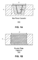
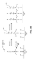
- FIGS. 1A and 1B illustrate capacitor architecture according to an embodiment.
- an on package capacitor is generated in a non-planar architecture, thus allow an increase in area plate area and capacitance while not increasing the X-Y space required for the on package capacitor.
- a capacitor 100 is a non-planar shaped on package capacitor, the non-planar capacitor 100 including a height h, diameter D, and spacing distance S for the capacitor, with a dielectric material having dielectric constant k being between the plates,
- capacitor 100 in FIG. 1A is illustrated as a capacitor with a conical or cylindrical shape, embodiments are not limited to these shapes, but rather also include any other non-planar shape that can be fabricated in the via, which may also include a pyramidal shape, a polyhedral shape, or irregular shape.
- FIG. 1B illustrates a conventional parallel plate on package capacitor, the capacitor also including a diameter D and height h.
- the non-planar capacitor includes a significantly larger plate area and significantly smaller spacing distance because of the non-planar construction of the device.
- a metallization process allows for fabrication of non-planar capacitors, including capacitors of conical, cylindrical, or other nonplanar shapes.
- the capacitance density can be greatly increased by making the dielectric separation layer much smaller than the layer thickness, an arrangement that is not available to parallel plate capacitors where the separation is dictated by other package design considerations.
- the capacitance per unit area is inversely proportional to the separation distance S, as provided in Equation 1:
- an embodiment of an on-package conical or cylindrical capacitors will have a capacitance density that is higher than parallel plate on-package capacitors density by a factor roughly proportional to the aspect ratio.
- F the capacitance per lateral area unit is increased by a factor F equal to:
- the resultant capacitance per unit lateral area is 7.7 ⁇ 10 ⁇ 4 F/mm 2 for the conical or cylindrical capacitor and 1.8 ⁇ 10 ⁇ 6 F/mm 2 for the parallel-plate equivalent.
- the capacitance of the non-planar device may have more than twice the capacitance density compared to traditional planar MIM capacitors on package.
- the capacitance density may be high enough to enable on-package capacitances for certain power delivery applications.
- decoupling capacitors for many electronic circuits may vary between 100 pF and 10 nF.
- a non-planar package integrated capacitor may be implemented in many RF and digital circuits, or in power delivery in certain implementations, without need for significant additional assembly in comparison with discrete passives.
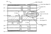
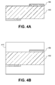
- FIG. 2 is an illustration of a package including an on package capacitor.
- a particular package 200 includes multiple layers, illustrated as, from a core 240 , layers 1F through 4F (up from the core) and 1B through 4B (down from the core).
- the package may include Ni/Au (Nickel/gold) plating at 4F, and copper plating at 4F, 3F, and 2F.
- the package includes an embedded (integrated) capacitor 250 including first copper plate 220 , second copper plate 225 at 1F, and between the plates a high k thin film dielectric 230 , with a via providing connection to 2F.
- the embedded capacitor utilizes conventional parallel plates, thus providing limited capacitance.
- the embedded capacitor may instead include a non-planer capacitor, such as a conical or cylindrical capacitor 100 as illustrated in FIG. 1A .
- a process is provided to generate a conical, cylindrical, or other non-planar shape, including the provision of effective plating of the surface of the non-planar shape.
- FIG. 3A illustrates a process for SAM assisted e-less plating for generation of an on package capacitor according to an embodiment.
- a non-planar on package capacitor is generated utilizing SAM (Self Aligned Monolayer) assisted e-less (electro-less) plating, wherein the plating process includes the following:
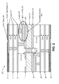
- FIG. 3B illustrates siloxane SAM grafting on activated substrates for generation of an on package capacitor according to an embodiment.
- a process for grafting a functional group R 350 onto an activated substrate 360 includes performance of hydrolysis on a hydrolysable group 355 to form a combined molecule 370 .
- the grafting process further includes condensation, resulting in the grating of the condensed molecule 375 onto the substrate 360 .
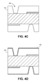
- FIGS. 4A through 4L illustrate the fabrication of an embedded non-planar capacitor according to an embodiment.
- the fabrication of an embedded non-planar capacitor includes the following:
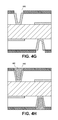
- FIG. 4A A substrate core 400 is clad with copper 405 .
- FIG. 4B Laminate build up material 410 is applied, wherein the laminate material may include build-up layer dielectric film.
- FIG. 4C A laser is applied to form vias 420 .
- FIG. 4D Electro-less plating to provide for forming of seed layer 425 over the surface of the laminate material 410 .
- the electro-less plating is SAM assisted electro-less plating.
- FIG. 4E Photo imaging resist 430 is laminated on the seed layer 425 .
- FIG. 4F Photo imaging patterning of the vias 435 .
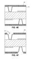
- FIG. 4G Electrolytic copper plating 440 of the vias.
- FIG. 4H Polymer 445 is applied over the copper plating 440 of the vias to provide a capacitor dielectric.
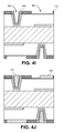
- FIG. 4I Laser drilling of the polymer dielectric 445 to form a cavity 450 together with forming of trace location 455 in the photo imaging resist 430 .
- FIG. 4J SAM assisted electro-less plating, such as illustrated in FIG. 3A , of laser drilled area for copper seeding, and electrolytic copper plating to fill the via cavities 460 and trace 465 .
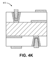
- FIG. 4K Resist stripping and seed removal, completing fabrication of the non-planar embedded capacitor 470 , wherein the capacitor in the embodiment is formed as a conical, cylindrical, pyramidal, polyhedral, or irregular shaped non-planar capacitor.
- the capacitor in the embodiment is formed as a conical, cylindrical, pyramidal, polyhedral, or irregular shaped non-planar capacitor.
- embodiments of non-planar capacitors are not limited to these shapes.
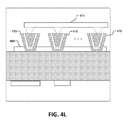
- FIG. 4L In some embodiments, a set of multiple non-planar capacitors 470 may be formed. In some embodiments, the multiple non-planar capacitors may be interconnected, as shown by an interconnection 475 of a first plate of each of the non-planar capacitors 470 and an interconnection 480 of a second plate of each of the non-planar capacitors 470 . In some embodiments, the interconnection of the non-planar capacitors includes one of a series interconnection or a parallel interconnection of the non-planar capacitors.
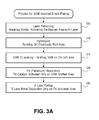
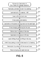
- FIG. 5 is a flowchart to illustrate a process for fabrication of a non-planar on package capacitor according to an embodiment.
- a process for fabricating a non-planar capacitor includes:
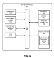
- FIG. 6 is an illustration of a system including one or more embedded non-planar capacitors according to an embodiment. In this illustration, certain standard and well-known components that are not germane to the present description are not shown.
- a system in package (SiP) or other system 600 includes one or more passive devices 650 , wherein the passive devices 650 include one or more non-planar embedded capacitors 655 , wherein the capacitors 655 may include capacitors fabricated in a package as illustrated in FIGS. 4A through 4L , or in a process as illustrated in FIG. 5 .
- the capacitors may include conical or cylindrical capacitors such as illustrated in FIG. 1A .
- the system 600 further includes a processing means such as one or more processors 610 coupled to one or more buses or interconnects, shown in general as bus 665 .
- the processors 610 may comprise one or more physical processors and one or more logical processors.
- the processors may include one or more general-purpose processors or special-processor processors.
- the bus 665 is a communication means for transmission of data.
- the bus 665 is illustrated as a single bus for simplicity, but may represent multiple different interconnects or buses and the component connections to such interconnects or buses may vary.
- the bus 665 shown in FIG. 6 is an abstraction that represents any one or more separate physical buses, point-to-point connections, or both connected by appropriate bridges, adapters, or controllers.
- the system 600 further comprises a random access memory (RAM) or other dynamic storage device or element as a main memory 615 for storing information and instructions to be executed by the processors 610 .
- Main memory 615 may include, but is not limited to, dynamic random access memory (DRAM).
- the system 600 also may comprise a non-volatile memory 620 ; and a read only memory (ROM) 635 or other static storage device for storing static information and instructions for the processors 610 .
- ROM read only memory
- the system 600 includes one or more transmitters or receivers 640 coupled to the bus 665 .
- the system 600 may include one or more antennae 644 , such as dipole or monopole antennae, for the transmission and reception of data via wireless communication using a wireless transmitter, receiver, or both, and one or more ports 642 for the transmission and reception of data via wired communications.
- Wireless communication includes, but is not limited to, Wi-Fi, BluetoothTM, near field communication, and other wireless communication standards.
- Various embodiments may include various processes. These processes may be performed by hardware components or may be embodied in computer program or machine-executable instructions, which may be used to cause a general-purpose or special-purpose processor or logic circuits programmed with the instructions to perform the processes. Alternatively, the processes may be performed by a combination of hardware and software.
- Portions of various embodiments may be provided as a computer program product, which may include a computer-readable medium having stored thereon computer program instructions, which may be used to program a computer (or other electronic devices) for execution by one or more processors to perform a process according to certain embodiments.
- the computer-readable medium may include, but is not limited to, magnetic disks, optical disks, read-only memory (ROM), random access memory (RAM), erasable programmable read-only memory (EPROM), electrically-erasable programmable read-only memory (EEPROM), magnetic or optical cards, flash memory, or other type of computer-readable medium suitable for storing electronic instructions.
- embodiments may also be downloaded as a computer program product, wherein the program may be transferred from a remote computer to a requesting computer.
- element A may be directly coupled to element B or be indirectly coupled through, for example, element C.
- a component, feature, structure, process, or characteristic A “causes” a component, feature, structure, process, or characteristic B, it means that “A” is at least a partial cause of “B” but that there may also be at least one other component, feature, structure, process, or characteristic that assists in causing “B.” If the specification indicates that a component, feature, structure, process, or characteristic “may”, “might”, or “could” be included, that particular component, feature, structure, process, or characteristic is not required to be included. If the specification or claim refers to “a” or “an” element, this does not mean there is only one of the described elements.
- An embodiment is an implementation or example.
- Reference in the specification to “an embodiment,” “one embodiment,” “some embodiments,” or “other embodiments” means that a particular feature, structure, or characteristic described in connection with the embodiments is included in at least some embodiments, but not necessarily all embodiments.
- the various appearances of “an embodiment,” “one embodiment,” or “some embodiments” are not necessarily all referring to the same embodiments. It should be appreciated that in the foregoing description of exemplary embodiments, various features are sometimes grouped together in a single embodiment, figure, or description thereof for the purpose of streamlining the disclosure and aiding in the understanding of one or more of the various novel aspects. This method of disclosure, however, is not to be interpreted as reflecting an intention that the claimed embodiments requires more features than are expressly recited in each claim. Rather, as the following claims reflect, novel aspects lie in less than all features of a single foregoing disclosed embodiment. Thus, the claims are hereby expressly incorporated into this description, with each claim standing on its own as a separate embodiment.
- an embedded capacitor includes a first plate formed in a package via; a dielectric material layer applied on the first plate; and a second plate formed in a cavity in the dielectric layer, wherein the first plate and the second plate are non-planar plates.
- the first plate and the second plate are conical, cylindrical, pyramidal, polyhedral, or irregular in shape.
- the first plate is a plate formed by electro-less plating to form a seed layer and electrolytic plating on the seed layer.
- the electro-less plating of the first plate includes SAM (Self-Assembled Monolayer) assisted electro-less plating.
- the cavity in the dielectric layer is a laser drilled cavity.
- the second plate is a plate formed by electro-less plating of the cavity and electrolytic plating to fill the cavity.
- the electro-less plating of the cavity includes SAM (Self-Assembled Monolayer) assisted electro-less plating.
- the electro-less plating includes laser patterning of the dielectric material layer.
- a method to form a non-planar via capacitor includes applying laminate build up on a package core; forming a first via with a laser; applying a first copper plating to form a first plate within the first via; filling the first via with a dielectric material; laser drilling of the dielectric material to form a cavity; and filling the cavity with a second copper plating to form a second plate.
- applying the first copper plating to form the first plate includes performing electro-less plating to generate a seed layer; and performing electrolytic plating to form the first plate.
- the electro-less plating of the first plate includes SAM (Self-Assembled Monolayer) assisted electro-less plating.
- filling the cavity with the second copper plating to form the second plate includes performing electro-less plating to generate a seed layer on the dielectric material; and performing electrolytic plating to form the second plate.
- performing electro-less plating to generate the seed layer on the dielectric material includes performing laser patterning of the dielectric material to break molecular bonds within the dielectric material.
- performing electro-less plating to generate the seed layer on the dielectric material includes forming an —OH (hydroxyl) rich area on the dielectric material; and grafting a SAM (Self Aligned Monolayer) onto the —OH rich area.
- —OH hydroxyl
- SAM Self Aligned Monolayer
- the SAM monolayer selectively allows adsorption of a plating-promoting catalyst to promote plating.
- forming the first plate and the second plate includes forming non-planar plates. In some embodiments, forming the first plate and the second plate includes forming conical, cylindrical, pyramidal, polyhedral, or irregular plates.
- a system in package includes one or more processors in a package for processing data; a transmitter, receiver, or both in the package for communication of data using one or more antennae; and one or more passive components embedded in the package, the one or more passive components including a first non-planar via capacitor, wherein the first non-planar via capacitor includes a first plate formed in a first via of the package, a dielectric layer applied on the first plate, and a second plate formed in a cavity in the dielectric layer, wherein the first plate and the second plate of the first non-planar via capacitor are non-planar plates.
- the first plate and the second plate of the first non-planar via capacitor are conical, cylindrical, pyramidal, polyhedral, or irregular in shape.
- the first plate of the first non-planar via capacitor is a plate formed by electro-less plating to form a seed layer and electrolytic plating on the seed layer.
- the electro-less plating of the first plate includes SAM (Self-Assembled Monolayer) assisted electro-less plating.
- the cavity in the dielectric layer is a laser drilled cavity.
- the second plate of the first non-planar via capacitor is a plated formed by electro-less plating of the cavity and electrolytic plating to fill the cavity.
- the electro-less plating of the cavity includes SAM (Self-Assembled Monolayer) assisted electro-less plating.
- the one or more passive components embedded in the package include a plurality of non-planar via capacitors, the plurality of non-planar via capacitors being interconnected.
- the interconnection of the plurality of non-planar via capacitors is one of a series interconnection or a parallel interconnection.
Landscapes
- Engineering & Computer Science (AREA)
- Microelectronics & Electronic Packaging (AREA)
- Manufacturing & Machinery (AREA)
- Fixed Capacitors And Capacitor Manufacturing Machines (AREA)
- Physics & Mathematics (AREA)
- Geometry (AREA)
- Ceramic Capacitors (AREA)
- Optics & Photonics (AREA)
Abstract
Description
- Embodiments described herein generally relate to the field of electronic devices and, more particularly, a non-planar on-package via capacitor.
- Modern wireless communication systems utilize several passive networks for matching and filtering. At radio frequencies (RF), the most critical passive components are inductors and capacitors. The filtering and matching circuits, which include transformers, baluns, filters, diplexers among others, can be fabricated as an integrated passive device (IPD) using silicon, glass, LTCC (Low Temperature Co-fired Ceramic), or other semiconducting substrate and then attached/assembled on the package. Alternatively, such circuits can be fabricated as part of the organic package or PCB (Printed Circuit Board) substrate. Direct fabrication of the passives on the package removes the need for assembly, and can allow package height reduction.
- Metal-insulator-metal (MIM) capacitors on package have been demonstrated using high-k material sandwiched between planar metal layers. In this arrangement, the high-k dielectric layer is thinner than the other (build-up) dielectric layers of the package.
- However, the density of on-package MIM capacitors have been limited by (1) the electrode surface area that is available, (2) the need for signal escape using vias and associated large via pads.
- Embodiments described here are illustrated by way of example, and not by way of limitation, in the figures of the accompanying drawings in which like reference numerals refer to similar elements.
-
FIGS. 1A and 1B illustrate capacitor architecture according to an embodiment; -
FIG. 2 is an illustration of a package including an on package capacitor; -
FIG. 3A illustrates a process for SAM assisted e-less plating for generation of an on package capacitor according to an embodiment; -
FIG. 3B illustrates siloxane SAM grafting on activated substrates for generation of an on package capacitor according to an embodiment; -
FIGS. 4A through 4L illustrate the fabrication of an embedded non-planar capacitor according to an embodiment; -
FIG. 5 is a flowchart to illustrate a process for fabrication of a non-planar on package capacitor according to an embodiment; and -
FIG. 6 is an illustration of a system including one or more embedded non-planar capacitors according to an embodiment. - Embodiments described herein are generally directed to a non-planar on-package via capacitor.
- As used herein, the following apply:
- “Capacitance density” refers to capacitance per lateral area unit.
- In some embodiments, an apparatus, system, or process provides for a non-planar on package via capacitor. In some embodiments, the non-planar on package via capacitor is fabricated in a package using a SAM (Self-Assembled Monolayers) assisted Laser direct structuring process. The implementation of a non-planar on package via capacitor enables a significant increase in capacitance by increasing the plate area and reducing plate distance without increasing the area required for capacitors.
- While most RF applications utilize capacitors in the order of fF (femtofarads, ×10−15) to a few pF (picofarads, ×10−12), enabling high density (for example 10-30 pF/mm2) capacitance can assist significantly with the circuit size reduction, and further help with the reduction of parasitic inductance in a circuit. Parasitic inductance increases the capacitance self-resonance frequency, and therefore limits applicability for broadband (with respect to frequency bandwidth) circuit implementation.
-
FIGS. 1A and 1B illustrate capacitor architecture according to an embodiment. In some embodiments, an on package capacitor is generated in a non-planar architecture, thus allow an increase in area plate area and capacitance while not increasing the X-Y space required for the on package capacitor. As illustrated inFIG. 1A , in an embodiment acapacitor 100 is a non-planar shaped on package capacitor, thenon-planar capacitor 100 including a height h, diameter D, and spacing distance S for the capacitor, with a dielectric material having dielectric constant k being between the plates, - While the
particular capacitor 100 inFIG. 1A is illustrated as a capacitor with a conical or cylindrical shape, embodiments are not limited to these shapes, but rather also include any other non-planar shape that can be fabricated in the via, which may also include a pyramidal shape, a polyhedral shape, or irregular shape. - In comparison,
FIG. 1B illustrates a conventional parallel plate on package capacitor, the capacitor also including a diameter D and height h. However, the non-planar capacitor includes a significantly larger plate area and significantly smaller spacing distance because of the non-planar construction of the device. - In some embodiments, a metallization process allows for fabrication of non-planar capacitors, including capacitors of conical, cylindrical, or other nonplanar shapes. For these geometries, the capacitance density can be greatly increased by making the dielectric separation layer much smaller than the layer thickness, an arrangement that is not available to parallel plate capacitors where the separation is dictated by other package design considerations. The capacitance per unit area is inversely proportional to the separation distance S, as provided in Equation 1:
-
- Because of the inverse proportion of capacitance to separation distance, the decrease in separation distance will scale the capacitance density.
- Further, an embodiment of an on-package conical or cylindrical capacitors will have a capacitance density that is higher than parallel plate on-package capacitors density by a factor roughly proportional to the aspect ratio. For conical or cylindrical shaped capacitors, assuming the separation distance is much smaller than both the height and diameter, the capacitance per lateral area unit is increased by a factor F equal to:
-
- In a particular example, assuming a separation distance s=200 nm for a conical capacitor, a dielectric constant of 3.0, a capacitor height of h=15 μm, a parallel plate capacitor separation distance of h=15 μm, a sidewall angle of θ=80°, and a capacitor diameter D of 30 μm, the resultant capacitance per unit lateral area is 7.7×10⁻⁴ F/mm2 for the conical or cylindrical capacitor and 1.8×10⁻⁶ F/mm2 for the parallel-plate equivalent.
- A non-planar via capacitor according to an embodiment may provide the following:
- (a) The capacitance of the non-planar device may have more than twice the capacitance density compared to traditional planar MIM capacitors on package.
- (b) In an embodiment in which the vertical capacitance structure is combined with high-k dielectric materials, the capacitance density may be high enough to enable on-package capacitances for certain power delivery applications. For example, decoupling capacitors for many electronic circuits may vary between 100 pF and 10 nF.
- (c) A non-planar package integrated capacitor may be implemented in many RF and digital circuits, or in power delivery in certain implementations, without need for significant additional assembly in comparison with discrete passives.
-
FIG. 2 is an illustration of a package including an on package capacitor. As illustrated inFIG. 2 , aparticular package 200 includes multiple layers, illustrated as, from acore 240,layers 1F through 4F (up from the core) and 1B through 4B (down from the core). Among other elements, the package may include Ni/Au (Nickel/gold) plating at 4F, and copper plating at 4F, 3F, and 2F. The package includes an embedded (integrated)capacitor 250 includingfirst copper plate 220,second copper plate 225 at 1F, and between the plates a high k thin film dielectric 230, with a via providing connection to 2F. As shown, the embedded capacitor utilizes conventional parallel plates, thus providing limited capacitance. - In some embodiments, rather than utilizing parallel plates as illustrated in
FIG. 2 , the embedded capacitor may instead include a non-planer capacitor, such as a conical orcylindrical capacitor 100 as illustrated inFIG. 1A . - In some embodiments, in order to provide enhanced capacitance in a package without requiring additional package space, a process is provided to generate a conical, cylindrical, or other non-planar shape, including the provision of effective plating of the surface of the non-planar shape.
-
FIG. 3A illustrates a process for SAM assisted e-less plating for generation of an on package capacitor according to an embodiment. In some embodiments, a non-planar on package capacitor is generated utilizing SAM (Self Aligned Monolayer) assisted e-less (electro-less) plating, wherein the plating process includes the following: -
- 305: Laser patterning—In order to break molecular bonds within a material, activating the desired area with a laser.
- 310: Hydrolysis—Forming an —OH (hydroxyl) rich area.
- 315: SAM (1) soaking—Grafting SAM onto the —OH rich area.
- 320: Pd (Palladium) absorption—A palladium catalyst is activated only on the SAM grafted area.
- 325: E-less plating—Electro-less metal deposition only on the Pd activated area.
-
FIG. 3B illustrates siloxane SAM grafting on activated substrates for generation of an on package capacitor according to an embodiment. As illustrated inFIG. 3B , a process for grafting afunctional group R 350 onto an activatedsubstrate 360 includes performance of hydrolysis on ahydrolysable group 355 to form a combinedmolecule 370. The grafting process further includes condensation, resulting in the grating of thecondensed molecule 375 onto thesubstrate 360. -
FIGS. 4A through 4L illustrate the fabrication of an embedded non-planar capacitor according to an embodiment. In some embodiments, the fabrication of an embedded non-planar capacitor includes the following: -
FIG. 4A : Asubstrate core 400 is clad withcopper 405. -
FIG. 4B : Laminate build upmaterial 410 is applied, wherein the laminate material may include build-up layer dielectric film. -
FIG. 4C : A laser is applied to formvias 420. -
FIG. 4D : Electro-less plating to provide for forming ofseed layer 425 over the surface of thelaminate material 410. In some embodiments, the electro-less plating is SAM assisted electro-less plating. -
FIG. 4E : Photo imaging resist 430 is laminated on theseed layer 425. -
FIG. 4F : Photo imaging patterning of thevias 435. -
FIG. 4G : Electrolytic copper plating 440 of the vias. -
FIG. 4H :Polymer 445 is applied over the copper plating 440 of the vias to provide a capacitor dielectric. -
FIG. 4I : Laser drilling of thepolymer dielectric 445 to form acavity 450 together with forming oftrace location 455 in the photo imaging resist 430. -
FIG. 4J : SAM assisted electro-less plating, such as illustrated inFIG. 3A , of laser drilled area for copper seeding, and electrolytic copper plating to fill the viacavities 460 andtrace 465. -
FIG. 4K : Resist stripping and seed removal, completing fabrication of the non-planar embeddedcapacitor 470, wherein the capacitor in the embodiment is formed as a conical, cylindrical, pyramidal, polyhedral, or irregular shaped non-planar capacitor. However, embodiments of non-planar capacitors are not limited to these shapes. -
FIG. 4L : In some embodiments, a set of multiplenon-planar capacitors 470 may be formed. In some embodiments, the multiple non-planar capacitors may be interconnected, as shown by aninterconnection 475 of a first plate of each of thenon-planar capacitors 470 and aninterconnection 480 of a second plate of each of thenon-planar capacitors 470. In some embodiments, the interconnection of the non-planar capacitors includes one of a series interconnection or a parallel interconnection of the non-planar capacitors. -
FIG. 5 is a flowchart to illustrate a process for fabrication of a non-planar on package capacitor according to an embodiment. In some embodiments, a process for fabricating a non-planar capacitor includes: -
- 505: Fabricate substrate core with copper cladding.
- 510: Laminate build up material on the substrate core, wherein the laminate material may include build-up dielectric film.
- 515: Laser drilling of the laminate material to form vias.
- 520: Perform electro-less plating and forming of seed layer over the surface of the laminate material.
- 525: Lamination of photo imaging resist on the seed layer.
- 530: Perform photo imaging patterning of the vias.
- 535: Perform electrolytic copper plating of the vias.
- 540: Application of polymer to fill the vias for a capacitor dielectric.
- 545: Laser drilling of the polymer filling in the vias to form cavities.
- 550: Perform SAM assisted electro-less plating of laser drilled area for copper seeding.
- 555: Perform electrolytic copper plating to fill the via cavities.
- 560: Resist stripping and seed removal to complete fabrication of the non-planar embedded capacitor.
-
FIG. 6 is an illustration of a system including one or more embedded non-planar capacitors according to an embodiment. In this illustration, certain standard and well-known components that are not germane to the present description are not shown. - In some embodiments, a system in package (SiP) or
other system 600 includes one or morepassive devices 650, wherein thepassive devices 650 include one or more non-planar embeddedcapacitors 655, wherein thecapacitors 655 may include capacitors fabricated in a package as illustrated inFIGS. 4A through 4L , or in a process as illustrated inFIG. 5 . In some embodiments, the capacitors may include conical or cylindrical capacitors such as illustrated inFIG. 1A . - In some embodiments, the
system 600 further includes a processing means such as one ormore processors 610 coupled to one or more buses or interconnects, shown in general as bus 665. Theprocessors 610 may comprise one or more physical processors and one or more logical processors. In some embodiments, the processors may include one or more general-purpose processors or special-processor processors. - The bus 665 is a communication means for transmission of data. The bus 665 is illustrated as a single bus for simplicity, but may represent multiple different interconnects or buses and the component connections to such interconnects or buses may vary. The bus 665 shown in
FIG. 6 is an abstraction that represents any one or more separate physical buses, point-to-point connections, or both connected by appropriate bridges, adapters, or controllers. - In some embodiments, the
system 600 further comprises a random access memory (RAM) or other dynamic storage device or element as amain memory 615 for storing information and instructions to be executed by theprocessors 610.Main memory 615 may include, but is not limited to, dynamic random access memory (DRAM). - The
system 600 also may comprise anon-volatile memory 620; and a read only memory (ROM) 635 or other static storage device for storing static information and instructions for theprocessors 610. - In some embodiments, the
system 600 includes one or more transmitters orreceivers 640 coupled to the bus 665. In some embodiments, thesystem 600 may include one ormore antennae 644, such as dipole or monopole antennae, for the transmission and reception of data via wireless communication using a wireless transmitter, receiver, or both, and one ormore ports 642 for the transmission and reception of data via wired communications. Wireless communication includes, but is not limited to, Wi-Fi, Bluetooth™, near field communication, and other wireless communication standards. - In the description above, for the purposes of explanation, numerous specific details are set forth in order to provide a thorough understanding of the described embodiments. It will be apparent, however, to one skilled in the art that embodiments may be practiced without some of these specific details. In other instances, well-known structures and devices are shown in block diagram form. There may be intermediate structure between illustrated components. The components described or illustrated herein may have additional inputs or outputs that are not illustrated or described.
- Various embodiments may include various processes. These processes may be performed by hardware components or may be embodied in computer program or machine-executable instructions, which may be used to cause a general-purpose or special-purpose processor or logic circuits programmed with the instructions to perform the processes. Alternatively, the processes may be performed by a combination of hardware and software.
- Portions of various embodiments may be provided as a computer program product, which may include a computer-readable medium having stored thereon computer program instructions, which may be used to program a computer (or other electronic devices) for execution by one or more processors to perform a process according to certain embodiments. The computer-readable medium may include, but is not limited to, magnetic disks, optical disks, read-only memory (ROM), random access memory (RAM), erasable programmable read-only memory (EPROM), electrically-erasable programmable read-only memory (EEPROM), magnetic or optical cards, flash memory, or other type of computer-readable medium suitable for storing electronic instructions. Moreover, embodiments may also be downloaded as a computer program product, wherein the program may be transferred from a remote computer to a requesting computer.
- Many of the methods are described in their most basic form, but processes can be added to or deleted from any of the methods and information can be added or subtracted from any of the described messages without departing from the basic scope of the present embodiments. It will be apparent to those skilled in the art that many further modifications and adaptations can be made. The particular embodiments are not provided to limit the concept but to illustrate it. The scope of the embodiments is not to be determined by the specific examples provided above but only by the claims below.
- If it is said that an element “A” is coupled to or with element “B,” element A may be directly coupled to element B or be indirectly coupled through, for example, element C. When the specification or claims state that a component, feature, structure, process, or characteristic A “causes” a component, feature, structure, process, or characteristic B, it means that “A” is at least a partial cause of “B” but that there may also be at least one other component, feature, structure, process, or characteristic that assists in causing “B.” If the specification indicates that a component, feature, structure, process, or characteristic “may”, “might”, or “could” be included, that particular component, feature, structure, process, or characteristic is not required to be included. If the specification or claim refers to “a” or “an” element, this does not mean there is only one of the described elements.
- An embodiment is an implementation or example. Reference in the specification to “an embodiment,” “one embodiment,” “some embodiments,” or “other embodiments” means that a particular feature, structure, or characteristic described in connection with the embodiments is included in at least some embodiments, but not necessarily all embodiments. The various appearances of “an embodiment,” “one embodiment,” or “some embodiments” are not necessarily all referring to the same embodiments. It should be appreciated that in the foregoing description of exemplary embodiments, various features are sometimes grouped together in a single embodiment, figure, or description thereof for the purpose of streamlining the disclosure and aiding in the understanding of one or more of the various novel aspects. This method of disclosure, however, is not to be interpreted as reflecting an intention that the claimed embodiments requires more features than are expressly recited in each claim. Rather, as the following claims reflect, novel aspects lie in less than all features of a single foregoing disclosed embodiment. Thus, the claims are hereby expressly incorporated into this description, with each claim standing on its own as a separate embodiment.
- In some embodiments, an embedded capacitor includes a first plate formed in a package via; a dielectric material layer applied on the first plate; and a second plate formed in a cavity in the dielectric layer, wherein the first plate and the second plate are non-planar plates.
- In some embodiments, the first plate and the second plate are conical, cylindrical, pyramidal, polyhedral, or irregular in shape.
- In some embodiments, the first plate is a plate formed by electro-less plating to form a seed layer and electrolytic plating on the seed layer.
- In some embodiments, the electro-less plating of the first plate includes SAM (Self-Assembled Monolayer) assisted electro-less plating.
- In some embodiments, the cavity in the dielectric layer is a laser drilled cavity.
- In some embodiments, the second plate is a plate formed by electro-less plating of the cavity and electrolytic plating to fill the cavity.
- In some embodiments, the electro-less plating of the cavity includes SAM (Self-Assembled Monolayer) assisted electro-less plating.
- In some embodiments, the electro-less plating includes laser patterning of the dielectric material layer.
- In some embodiments, a method to form a non-planar via capacitor includes applying laminate build up on a package core; forming a first via with a laser; applying a first copper plating to form a first plate within the first via; filling the first via with a dielectric material; laser drilling of the dielectric material to form a cavity; and filling the cavity with a second copper plating to form a second plate.
- In some embodiments, applying the first copper plating to form the first plate includes performing electro-less plating to generate a seed layer; and performing electrolytic plating to form the first plate.
- In some embodiments, the electro-less plating of the first plate includes SAM (Self-Assembled Monolayer) assisted electro-less plating.
- In some embodiments, filling the cavity with the second copper plating to form the second plate includes performing electro-less plating to generate a seed layer on the dielectric material; and performing electrolytic plating to form the second plate.
- In some embodiments, performing electro-less plating to generate the seed layer on the dielectric material includes performing laser patterning of the dielectric material to break molecular bonds within the dielectric material.
- In some embodiments, performing electro-less plating to generate the seed layer on the dielectric material includes forming an —OH (hydroxyl) rich area on the dielectric material; and grafting a SAM (Self Aligned Monolayer) onto the —OH rich area.
- In some embodiments, the SAM monolayer selectively allows adsorption of a plating-promoting catalyst to promote plating.
- In some embodiments, forming the first plate and the second plate includes forming non-planar plates. In some embodiments, forming the first plate and the second plate includes forming conical, cylindrical, pyramidal, polyhedral, or irregular plates.
- In some embodiments, a system in package includes one or more processors in a package for processing data; a transmitter, receiver, or both in the package for communication of data using one or more antennae; and one or more passive components embedded in the package, the one or more passive components including a first non-planar via capacitor, wherein the first non-planar via capacitor includes a first plate formed in a first via of the package, a dielectric layer applied on the first plate, and a second plate formed in a cavity in the dielectric layer, wherein the first plate and the second plate of the first non-planar via capacitor are non-planar plates.
- In some embodiments, the first plate and the second plate of the first non-planar via capacitor are conical, cylindrical, pyramidal, polyhedral, or irregular in shape.
- In some embodiments, the first plate of the first non-planar via capacitor is a plate formed by electro-less plating to form a seed layer and electrolytic plating on the seed layer.
- In some embodiments, the electro-less plating of the first plate includes SAM (Self-Assembled Monolayer) assisted electro-less plating.
- In some embodiments, the cavity in the dielectric layer is a laser drilled cavity.
- In some embodiments, the second plate of the first non-planar via capacitor is a plated formed by electro-less plating of the cavity and electrolytic plating to fill the cavity.
- In some embodiments, the electro-less plating of the cavity includes SAM (Self-Assembled Monolayer) assisted electro-less plating.
- In some embodiments, the one or more passive components embedded in the package include a plurality of non-planar via capacitors, the plurality of non-planar via capacitors being interconnected.
- In some embodiments, the interconnection of the plurality of non-planar via capacitors is one of a series interconnection or a parallel interconnection.
Claims (26)
Priority Applications (2)
| Application Number | Priority Date | Filing Date | Title |
|---|---|---|---|
| US15/283,352 US10595410B2 (en) | 2016-10-01 | 2016-10-01 | Non-planar on-package via capacitor |
| PCT/US2017/049226 WO2018063687A1 (en) | 2016-10-01 | 2017-08-29 | Non-planar on-package via capacitor |
Applications Claiming Priority (1)
| Application Number | Priority Date | Filing Date | Title |
|---|---|---|---|
| US15/283,352 US10595410B2 (en) | 2016-10-01 | 2016-10-01 | Non-planar on-package via capacitor |
Publications (2)
| Publication Number | Publication Date |
|---|---|
| US20180098428A1 true US20180098428A1 (en) | 2018-04-05 |
| US10595410B2 US10595410B2 (en) | 2020-03-17 |
Family
ID=61758569
Family Applications (1)
| Application Number | Title | Priority Date | Filing Date |
|---|---|---|---|
| US15/283,352 Active 2036-10-10 US10595410B2 (en) | 2016-10-01 | 2016-10-01 | Non-planar on-package via capacitor |
Country Status (2)
| Country | Link |
|---|---|
| US (1) | US10595410B2 (en) |
| WO (1) | WO2018063687A1 (en) |
Cited By (6)
| Publication number | Priority date | Publication date | Assignee | Title |
|---|---|---|---|---|
| WO2020081691A1 (en) * | 2018-10-16 | 2020-04-23 | Averatek Corporation | Method of manufacture for embedded ic chip directly connected to pcb |
| US10734236B2 (en) | 2017-03-31 | 2020-08-04 | Intel Corporation | Electronic devices with components formed by late binding using self-assembled monolayers |
| US10777538B2 (en) | 2017-03-31 | 2020-09-15 | Intel Corporation | System on package architecture including structures on die back side |
| US11410921B2 (en) * | 2018-08-21 | 2022-08-09 | Intel Corporation | Methods to incorporate thin film capacitor sheets (TFC-S) in the build-up films |
| DE102021112577A1 (en) | 2021-05-14 | 2022-11-17 | Infineon Technologies Ag | METHOD OF MAKING AN ELECTRICAL COMPONENT HOUSING WITH PLATEABLE ENCAPSULATION LAYERS |
| US12603222B1 (en) * | 2023-08-29 | 2026-04-14 | Hrl Laboratories, Llc | Ceramic body with embedded capacitor |
Citations (11)
| Publication number | Priority date | Publication date | Assignee | Title |
|---|---|---|---|---|
| US4685197A (en) * | 1986-01-07 | 1987-08-11 | Texas Instruments Incorporated | Fabricating a stacked capacitor |
| US20050006688A1 (en) * | 2001-12-04 | 2005-01-13 | Solo De Zaldivar Jose | Arrangement comprising a capacitor |
| US20070114634A1 (en) * | 2005-10-29 | 2007-05-24 | Stats Chippac Ltd. | Integrated passive device system |
| US7285490B2 (en) * | 2003-01-15 | 2007-10-23 | Infineon Technologies Ag | Method for the producing an integrated circuit bar arrangement, in particular comprising a capacitor assembly, in addition to an integrated circuit arrangement |
| US7538375B2 (en) * | 2006-04-05 | 2009-05-26 | Samsung Electronics Co., Ltd. | Capacitor structure of semiconductor device and method of fabricating the same |
| US20100041203A1 (en) * | 2008-08-14 | 2010-02-18 | Collins David S | Structure, Design Structure and Method of Manufacturing a Structure Having VIAS and High Density Capacitors |
| US8022548B2 (en) * | 2006-10-12 | 2011-09-20 | Atmel Corporation | Method for fabricating conducting plates for a high-Q MIM capacitor |
| US20120322394A1 (en) * | 2009-05-19 | 2012-12-20 | Broadcom Corporation | Method and System for a Reconfigurable Filter That is Utilized by a RF Transmitter and a RF Receiver Which are Integrated on a Single Substrate |
| US8710658B2 (en) * | 2011-11-18 | 2014-04-29 | Cambridge Silicon Radio Limited | Under bump passive components in wafer level packaging |
| US8809149B2 (en) * | 2012-12-12 | 2014-08-19 | Globalfoundries Inc. | High density serial capacitor device and methods of making such a capacitor device |
| US9178009B2 (en) * | 2012-10-10 | 2015-11-03 | Globalfoundries Inc. | Methods of forming a capacitor and contact structures |
Family Cites Families (4)
| Publication number | Priority date | Publication date | Assignee | Title |
|---|---|---|---|---|
| TWI283458B (en) | 2006-04-04 | 2007-07-01 | Promos Technologies Inc | Method for preparing a capacitor structure of a semiconductor memory |
| KR20090001383A (en) | 2007-06-29 | 2009-01-08 | 삼성전자주식회사 | Method of manufacturing a capacitor |
| US8129267B2 (en) | 2008-03-21 | 2012-03-06 | International Business Machines Corporation | Alpha particle blocking wire structure and method fabricating same |
| US9373678B2 (en) | 2014-06-17 | 2016-06-21 | Globalfoundries Inc. | Non-planar capacitors with finely tuned capacitance values and methods of forming the non-planar capacitors |
-
2016
- 2016-10-01 US US15/283,352 patent/US10595410B2/en active Active
-
2017
- 2017-08-29 WO PCT/US2017/049226 patent/WO2018063687A1/en not_active Ceased
Patent Citations (11)
| Publication number | Priority date | Publication date | Assignee | Title |
|---|---|---|---|---|
| US4685197A (en) * | 1986-01-07 | 1987-08-11 | Texas Instruments Incorporated | Fabricating a stacked capacitor |
| US20050006688A1 (en) * | 2001-12-04 | 2005-01-13 | Solo De Zaldivar Jose | Arrangement comprising a capacitor |
| US7285490B2 (en) * | 2003-01-15 | 2007-10-23 | Infineon Technologies Ag | Method for the producing an integrated circuit bar arrangement, in particular comprising a capacitor assembly, in addition to an integrated circuit arrangement |
| US20070114634A1 (en) * | 2005-10-29 | 2007-05-24 | Stats Chippac Ltd. | Integrated passive device system |
| US7538375B2 (en) * | 2006-04-05 | 2009-05-26 | Samsung Electronics Co., Ltd. | Capacitor structure of semiconductor device and method of fabricating the same |
| US8022548B2 (en) * | 2006-10-12 | 2011-09-20 | Atmel Corporation | Method for fabricating conducting plates for a high-Q MIM capacitor |
| US20100041203A1 (en) * | 2008-08-14 | 2010-02-18 | Collins David S | Structure, Design Structure and Method of Manufacturing a Structure Having VIAS and High Density Capacitors |
| US20120322394A1 (en) * | 2009-05-19 | 2012-12-20 | Broadcom Corporation | Method and System for a Reconfigurable Filter That is Utilized by a RF Transmitter and a RF Receiver Which are Integrated on a Single Substrate |
| US8710658B2 (en) * | 2011-11-18 | 2014-04-29 | Cambridge Silicon Radio Limited | Under bump passive components in wafer level packaging |
| US9178009B2 (en) * | 2012-10-10 | 2015-11-03 | Globalfoundries Inc. | Methods of forming a capacitor and contact structures |
| US8809149B2 (en) * | 2012-12-12 | 2014-08-19 | Globalfoundries Inc. | High density serial capacitor device and methods of making such a capacitor device |
Cited By (8)
| Publication number | Priority date | Publication date | Assignee | Title |
|---|---|---|---|---|
| US10734236B2 (en) | 2017-03-31 | 2020-08-04 | Intel Corporation | Electronic devices with components formed by late binding using self-assembled monolayers |
| US10777538B2 (en) | 2017-03-31 | 2020-09-15 | Intel Corporation | System on package architecture including structures on die back side |
| US11410921B2 (en) * | 2018-08-21 | 2022-08-09 | Intel Corporation | Methods to incorporate thin film capacitor sheets (TFC-S) in the build-up films |
| WO2020081691A1 (en) * | 2018-10-16 | 2020-04-23 | Averatek Corporation | Method of manufacture for embedded ic chip directly connected to pcb |
| US12213258B2 (en) | 2018-10-16 | 2025-01-28 | Averatek Corporation | Method of manufacture for embedded IC chip directly connected to PCB |
| DE102021112577A1 (en) | 2021-05-14 | 2022-11-17 | Infineon Technologies Ag | METHOD OF MAKING AN ELECTRICAL COMPONENT HOUSING WITH PLATEABLE ENCAPSULATION LAYERS |
| DE102021112577B4 (en) | 2021-05-14 | 2023-06-01 | Infineon Technologies Ag | Process for the manufacture of an electrical component housing with platable encapsulation layers and such packaging |
| US12603222B1 (en) * | 2023-08-29 | 2026-04-14 | Hrl Laboratories, Llc | Ceramic body with embedded capacitor |
Also Published As
| Publication number | Publication date |
|---|---|
| WO2018063687A1 (en) | 2018-04-05 |
| US10595410B2 (en) | 2020-03-17 |
Similar Documents
| Publication | Publication Date | Title |
|---|---|---|
| US10595410B2 (en) | Non-planar on-package via capacitor | |
| CN113366628B (en) | Package substrate and semiconductor device including the same | |
| DE102015112980B4 (en) | THIN FILM CAPACITORS EMBEDDED IN HOUSING SUBSTRATES AND METHOD FOR INTEGRATING THIN FILM CAPACITORS EMBEDDED IN HOUSING SUBSTRATES | |
| US7550320B2 (en) | Method of fabricating substrate with embedded component therein | |
| US7763976B2 (en) | Integrated circuit module with integrated passive device | |
| CN111508692B (en) | Inductive components, packaged components, and switching regulators | |
| US8643179B2 (en) | Bump structure including nano-wires and a body connecting ends of the nano-wires, semiconductor package having the bump structure and method of manufacturing the semiconductor package | |
| CN103377818B (en) | A high-frequency component with through-hole inductance and its manufacturing method | |
| CN115918278A (en) | Multilayer wiring board and module having multilayer wiring board | |
| US7733662B2 (en) | Circuit board with embedded passive component and fabricating process thereof | |
| CN113990858B (en) | Integrated passive device, manufacturing method thereof and semiconductor device | |
| US20120028459A1 (en) | Manufacturing process of circuit substrate | |
| TW202013642A (en) | Semiconductor structure and manufacturing method thereof | |
| US7375022B2 (en) | Method of manufacturing wiring board | |
| CN102024565A (en) | Capacitor structure | |
| TWI437689B (en) | Semiconductor device | |
| US12094631B2 (en) | Chip inductor and method for manufacturing same | |
| US8884717B2 (en) | Diplexer | |
| US20090148962A1 (en) | Substrate structure and method for wideband power decoupling | |
| CN112713123A (en) | Semiconductor device package and method of manufacturing the same | |
| CN100584155C (en) | Substrate process for embedded components | |
| JP2005045112A (en) | Component built-in flexible circuit board and manufacturing method thereof | |
| US9461607B2 (en) | Balance filter | |
| KR102767539B1 (en) | Millimeter Wave Communication System using IPD | |
| US7776671B2 (en) | Inductor for semiconductor device and method of fabricating the same |
Legal Events
| Date | Code | Title | Description |
|---|---|---|---|
| AS | Assignment |
Owner name: INTEL CORPORATION, CALIFORNIA Free format text: ASSIGNMENT OF ASSIGNORS INTEREST;ASSIGNORS:HUA, FAY;RAWLINGS, BRANDON M.;DOGIAMIS, GEORGIOS C.;AND OTHERS;SIGNING DATES FROM 20161004 TO 20161010;REEL/FRAME:040992/0259 |
|
| STPP | Information on status: patent application and granting procedure in general |
Free format text: FINAL REJECTION MAILED |
|
| STPP | Information on status: patent application and granting procedure in general |
Free format text: RESPONSE AFTER FINAL ACTION FORWARDED TO EXAMINER |
|
| STPP | Information on status: patent application and granting procedure in general |
Free format text: ADVISORY ACTION MAILED |
|
| STPP | Information on status: patent application and granting procedure in general |
Free format text: DOCKETED NEW CASE - READY FOR EXAMINATION |
|
| STPP | Information on status: patent application and granting procedure in general |
Free format text: NON FINAL ACTION MAILED |
|
| STPP | Information on status: patent application and granting procedure in general |
Free format text: NOTICE OF ALLOWANCE MAILED -- APPLICATION RECEIVED IN OFFICE OF PUBLICATIONS |
|
| STPP | Information on status: patent application and granting procedure in general |
Free format text: AWAITING TC RESP., ISSUE FEE NOT PAID |
|
| STPP | Information on status: patent application and granting procedure in general |
Free format text: PUBLICATIONS -- ISSUE FEE PAYMENT VERIFIED |
|
| STCF | Information on status: patent grant |
Free format text: PATENTED CASE |
|
| MAFP | Maintenance fee payment |
Free format text: PAYMENT OF MAINTENANCE FEE, 4TH YEAR, LARGE ENTITY (ORIGINAL EVENT CODE: M1551); ENTITY STATUS OF PATENT OWNER: LARGE ENTITY Year of fee payment: 4 |