US20180098162A1 - Hearing assistance device incorporating system in package module - Google Patents
Hearing assistance device incorporating system in package module Download PDFInfo
- Publication number
- US20180098162A1 US20180098162A1 US15/285,299 US201615285299A US2018098162A1 US 20180098162 A1 US20180098162 A1 US 20180098162A1 US 201615285299 A US201615285299 A US 201615285299A US 2018098162 A1 US2018098162 A1 US 2018098162A1
- Authority
- US
- United States
- Prior art keywords
- substrate
- subsystem
- assistance device
- hearing assistance
- window
- Prior art date
- Legal status (The legal status is an assumption and is not a legal conclusion. Google has not performed a legal analysis and makes no representation as to the accuracy of the status listed.)
- Granted
Links
Images

Classifications
-
- H—ELECTRICITY
- H04—ELECTRIC COMMUNICATION TECHNIQUE
- H04R—LOUDSPEAKERS, MICROPHONES, GRAMOPHONE PICK-UPS OR LIKE ACOUSTIC ELECTROMECHANICAL TRANSDUCERS; ELECTRIC HEARING AIDS; PUBLIC ADDRESS SYSTEMS
- H04R25/00—Electric hearing aids
- H04R25/55—Electric hearing aids using an external connection, either wireless or wired
- H04R25/556—External connectors, e.g. plugs or modules
-
- H—ELECTRICITY
- H04—ELECTRIC COMMUNICATION TECHNIQUE
- H04R—LOUDSPEAKERS, MICROPHONES, GRAMOPHONE PICK-UPS OR LIKE ACOUSTIC ELECTROMECHANICAL TRANSDUCERS; ELECTRIC HEARING AIDS; PUBLIC ADDRESS SYSTEMS
- H04R25/00—Electric hearing aids
- H04R25/60—Mounting or interconnection of hearing aid parts, e.g. inside tips, housings or to ossicles
-
- H—ELECTRICITY
- H04—ELECTRIC COMMUNICATION TECHNIQUE
- H04R—LOUDSPEAKERS, MICROPHONES, GRAMOPHONE PICK-UPS OR LIKE ACOUSTIC ELECTROMECHANICAL TRANSDUCERS; ELECTRIC HEARING AIDS; PUBLIC ADDRESS SYSTEMS
- H04R25/00—Electric hearing aids
- H04R25/50—Customised settings for obtaining desired overall acoustical characteristics
- H04R25/505—Customised settings for obtaining desired overall acoustical characteristics using digital signal processing
-
- H—ELECTRICITY
- H04—ELECTRIC COMMUNICATION TECHNIQUE
- H04R—LOUDSPEAKERS, MICROPHONES, GRAMOPHONE PICK-UPS OR LIKE ACOUSTIC ELECTROMECHANICAL TRANSDUCERS; ELECTRIC HEARING AIDS; PUBLIC ADDRESS SYSTEMS
- H04R25/00—Electric hearing aids
- H04R25/55—Electric hearing aids using an external connection, either wireless or wired
- H04R25/554—Electric hearing aids using an external connection, either wireless or wired using a wireless connection, e.g. between microphone and amplifier or using Tcoils
-
- H—ELECTRICITY
- H04—ELECTRIC COMMUNICATION TECHNIQUE
- H04R—LOUDSPEAKERS, MICROPHONES, GRAMOPHONE PICK-UPS OR LIKE ACOUSTIC ELECTROMECHANICAL TRANSDUCERS; ELECTRIC HEARING AIDS; PUBLIC ADDRESS SYSTEMS
- H04R25/00—Electric hearing aids
- H04R25/55—Electric hearing aids using an external connection, either wireless or wired
- H04R25/558—Remote control, e.g. of amplification, frequency
-
- H—ELECTRICITY
- H04—ELECTRIC COMMUNICATION TECHNIQUE
- H04R—LOUDSPEAKERS, MICROPHONES, GRAMOPHONE PICK-UPS OR LIKE ACOUSTIC ELECTROMECHANICAL TRANSDUCERS; ELECTRIC HEARING AIDS; PUBLIC ADDRESS SYSTEMS
- H04R25/00—Electric hearing aids
- H04R25/60—Mounting or interconnection of hearing aid parts, e.g. inside tips, housings or to ossicles
- H04R25/609—Mounting or interconnection of hearing aid parts, e.g. inside tips, housings or to ossicles of circuitry
-
- H—ELECTRICITY
- H04—ELECTRIC COMMUNICATION TECHNIQUE
- H04R—LOUDSPEAKERS, MICROPHONES, GRAMOPHONE PICK-UPS OR LIKE ACOUSTIC ELECTROMECHANICAL TRANSDUCERS; ELECTRIC HEARING AIDS; PUBLIC ADDRESS SYSTEMS
- H04R25/00—Electric hearing aids
- H04R25/30—Monitoring or testing of hearing aids, e.g. functioning, settings, battery power
- H04R25/305—Self-monitoring or self-testing
Definitions
- This application relates generally to hearing assistance devices and methods of making such devices.
- Hearing aids are electronic instruments that compensate for hearing losses by amplifying sound.
- the electronic components of a hearing aid typically include a microphone for receiving ambient sound, an amplifier for amplifying the microphone signal, a speaker for converting the amplified microphone signal to sound for the wearer, and a battery for powering the components.
- the hearing assistance device comprises an enclosure and a system in package (SIP) module disposed within the enclosure.
- the SIP module comprises a first substrate having a first surface and an opposing second surface.
- the first substrate supports a first subsystem configured to perform a first function.
- a second substrate having a first surface and an opposing second surface supports a second subsystem configured to perform a second function different from the first function.
- the second surfaces face each other and at least one of the second surfaces supports one or more components.
- An interconnect layer is separate from and bonded to and between the first and second substrates.
- the interconnect layer comprises a window and a region peripheral to the window.
- the window is sized to accommodate the one or more components and the peripheral region comprises electrical pathways for electrically connecting the first subsystem and the second subsystem.
- Some embodiments are directed to a hearing assistance device adapted for use in or on a wearer comprising an enclosure and an SIP module disposed within the enclosure.
- the SIP module comprises a radio subsystem and a digital signal processor (DSP) subsystem arranged in a vertically stacked configuration.
- the SIP module comprises a first substrate having a first surface and an opposing second surface. The second surface of the first substrate supports the radio subsystem.
- a second substrate comprises a plurality of flexible layers and has a first surface and an opposing second surface. At least a DSP module of the DSP subsystem is embedded in the second substrate. The second surfaces face each other.
- An interconnect layer is separate from and bonded to and between the first and second substrates.
- the interconnect layer comprises a window and a region peripheral to the window. The window is sized to accommodate at least the radio subsystem and the peripheral region comprising electrical pathways for electrically connecting the radio subsystem and the DSP subsystem.
- a hearing assistance device adapted for use in or on a wearer comprising an enclosure and a SIP module disposed within the enclosure.
- the SIP module comprises a first substrate having a first surface and an opposing second surface. The surface of the first substrate supports a radio subsystem.
- a second substrate comprises a plurality of flexible layers and has a first surface and an opposing second surface.
- a DSP subsystem is embedded in the second substrate.
- a non-volatile memory integrated circuit is embedded in the second substrate and separated from the DSP subsystem by at least one of the flexible layers.
- One or more surface mount components are coupled to the DSP subsystem and supported by the second surface of the second substrate. The second surfaces face each other.
- An interconnect layer is separate from and bonded to and between the first and second substrates.
- the interconnect layer comprises a window and a region peripheral to the window. The window is sized to accommodate the radio subsystem and the one or more surface mount components.
- the peripheral region comprises electrical pathways for electrically connecting the radio subsystem and
- FIG. 1B is a cross-sectional view of a SIP module comprising two double embedded subsystems for use in a hearing assistance device in accordance with various embodiments;
- FIG. 2 is a cross-sectional view showing details of a windowed interconnect layer of the SIP modules shown in FIGS. 1A and 1B in accordance with various embodiments;
- FIG. 3 is a cross-sectional view of a double embedded SIP module comprising a multiplicity of subsystems for use in a hearing assistance device in accordance with various embodiments;
- FIG. 4 illustrates details of the double embedded module shown in FIG. 3 in accordance with various embodiments
- FIG. 5 illustrates a SIP module incorporated in a representative hearing assistance device in accordance with various embodiments
- FIGS. 6A and 6B illustrate a substrate comprising a multiplicity of subsystems each including a double embedded module in accordance with various embodiments
- FIGS. 7A and 7B illustrate a substrate comprising a multiplicity of interconnect layer regions in accordance with various embodiments
- FIGS. 8A and 8B illustrate a substrate comprising a multiplicity of subsystems each including a module configured to perform one or more functions in accordance with various embodiments;
- FIGS. 9A and 9B illustrate a multiplicity of SIP modules constructed from the substrates shown in FIGS. 6A-8B in accordance with various embodiments.
- Hearing assistance devices such as hearing aids and hearables (e.g., wearable earphones), typically include an enclosure, such as a housing or shell, within which internal components are disposed.
- Typical internal components of a hearing assistance device can include a signal processor, memory, power management circuitry, one or more communication devices, one or more antennas, one or more microphones, and a receiver/speaker, for example.
- the housing or shell of a hearing assistance device has a size limitation based on the application. Specifically, devices that include an in-the-ear shell or an on-the-ear shell are constrained by the geometry of the inner or outer ear of the wearer.
- More advanced hearing assistance devices can incorporate a long-range communication device, such as a Bluetooth® transceiver, space for which must be allocated within the shell of the device.
- a long-range communication device such as a Bluetooth® transceiver
- Embodiments of the disclosure are directed to a hearing assistance device which incorporates a multiplicity of electronic subsystems configured in the form of a system in package (SIP) module.
- SIP system in package
- PoP package-on-package
- SIP module as used herein also refers to a PoP module or a combined SIP/PoP module.
- a hearing assistance device incorporates a multiplicity of integrated circuits or chips arranged in multiple layers as a SIP module. For example, a multiplicity of integrated circuits or chips can be arranged in a vertically stacked configuration as a SIP module.
- Embodiments of the disclosure are directed to a SIP module adapted for use in various types of hearing devices, including hearables, hearing assistance devices, and/or hearing aids, including but not limited to, behind-the-ear (BTE), in-the-ear (ITE), in-the-canal (ITC), receiver-in-canal (RIC), receiver-in-the-ear (RITE) or completely-in-the-canal (CIC) type hearing devices.
- BTE behind-the-ear
- ITE in-the-ear
- ITC in-the-canal
- RIC receiver-in-canal
- RITE receiver-in-the-ear
- CIC completely-in-the-canal
- hearing devices may include devices that reside substantially behind the ear or over the ear.
- a SIP module adapted for incorporation in a hearing assistance device includes at least two vertically stacked subsystems, each of which comprises at least one integrated circuit (IC).
- the IC or ICs of one of the vertically stacked subsystems of the SIP module is/are embedded into a flexible circuit substrate.
- the IC or ICs of other vertically stacked subsystems of the SIP module can be supported by a rigid substrate or a flexible circuit substrate.
- each of the vertically stacked subsystems can include one or more ICs embedded in a flexible circuit substrate.
- Embodiments of a SIP module incorporate an interconnect layer disposed between the vertically stacked subsystems.
- the interconnect layer comprises a discrete substrate having a window and a region peripheral to the window.
- the window of the interconnect layer is sized to accommodate one or more components mounted to or extending from internal surfaces of the vertically stacked subsystems.
- the peripheral region of the interconnect layer incorporates electrical pathways for electrically connecting the vertically stacked subsystems. Electrical contacts on an exterior surface or surfaces of the SIP module serve as input/output pads for establishing electrical connection with other components of the hearing assistance device, typically via a mother flexible circuit disposed within the shell.
- a SIP module that incorporates a multiplicity of vertically stacked subsystems each separated by a windowed interconnect layer provides for integration of a greater number of electronic components within the constrained space of an in- or on-the-ear hearing assistance device as compared to conventional packaging techniques.
- a SIP module implemented in accordance with the present disclosure can accommodate four integrated circuits or dies within the space of two ICs or dies using conventional packaging techniques.
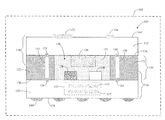
- FIG. 1A is a cross-sectional view of a SIP module comprising a multiplicity of subsystems for use in a hearing assistance device in accordance with various embodiments.
- FIG. 1A shows a SIP module 104 incorporated within a hearing assistance device 102 .
- the SIP module 104 includes a first subsystem 110 and a second subsystem 130 .
- the first subsystem 110 is a fully functional system that performs a first function
- the second subsystem 130 is a fully functional system that performs a second function.
- the first function performed by the first subsystem 110 is preferably different from the second function performed by the second subsystem 130 .
- the first function for example, may be a communication function
- the second function may be a signal processing function or a power management function.
- Other functions performed by the first and second subsystems 110 and 130 are contemplated, such as a biometric sensing function.
- the first subsystem 110 includes a first substrate 112 having a first surface 114 and an opposing second surface 116 .
- the first substrate 112 can be a rigid substrate or a flexible substrate with layers that interconnect via electrically conductive pathways or traces.
- the first substrate 112 can be a printed circuit board (PCB) formed from a rigid material such as bismaleimide-triazine (BT) resin, FR4 (e.g., glass-reinforced epoxy laminate) or other type of rigid PCB material.
- PCB printed circuit board
- the first surface 114 of the first substrate 112 supports one or more components 122 and 124 , which may be SMT (surface mount technology) components. Although two components 122 and 124 are shown populating the first surface 114 for illustrative purposes, it is understood that any number of components may be supported by the first surface 114 of the first substrate 112 .
- the second surface 116 of the first substrate 112 supports one or more components 120 .
- the one or more components 120 can include an SMT component, a flip-chip, a chip scale package-on-board (CSPOB) module, or a mix of these components/modules.
- CSPOB chip scale package-on-board
- the second subsystem 130 includes a second substrate 132 having a first surface 134 and an opposing second surface 136 .
- the second surface 136 of the second substrate 132 faces (e.g., is substantially parallel to) the second surface 116 of the first substrate 112 in a spaced-apart relationship.
- the second surface 136 of the second substrate 132 supports one or more components 138 and 140 (two components are shown for illustrative purposes), which may include any mix of SMT components, a flip-chip, and a CSPOB module.
- the second substrate 132 constitutes a flexible circuit substrate into which one or more components are embedded.
- the flexible circuit substrate may be constructed from films of a polyimide material.
- the second substrate 132 constitutes a flexible circuit board into which several integrated chips 135 and 137 of a module 133 are embedded vertically to define a wafer and board level device embedded package or WABE.
- the first surface 134 of the second substrate 132 includes a multiplicity of electrical contacts 180 .
- the electrical contacts 180 serve as user input/output (I/O) pads for the SIP module 104 .
- the electrical contacts 180 connect the SIP module 104 with other components of the hearing assistance device 102 , such as a battery, microphones, receiver, transceiver, and other components.
- the electrical contacts 180 may constitute electrically conductive traces, solder bumps or balls (e.g., a ball grid array or BGA), or other type of electrical contact.
- the electrical contacts 180 may be configured to allow for either BGA style gang reflow onto a mother flex circuit (see, e.g., FIG. 5 ) or individual hand wire soldering methods.
- the first and second subsystems 110 and 130 define a vertically stacked SIP structure, with each subsystem 110 , 130 supporting components that define a fully functioning system.
- An interconnect layer 150 is disposed between the first and second subsystems 110 and 130 .
- the interconnect layer 150 is a discrete layer that separates the first and second subsystems 110 and 130 .
- the interconnect layer 150 can constitute a substrate formed from a rigid material such as BT resin or FR4. In some embodiments the interconnect layer 150 can constitute a flexible substrate, such as one formed from polyimide or another suitable flexible substrate material.
- the interconnect layer 150 includes a window 170 (e.g., an aperture or void) and a solid region 172 peripheral to the window 170 .
- the window 170 is sized to accommodate the components 120 , 138 , 140 supported by the spaced-apart and opposing second surfaces 116 and 136 of the first and second substrates 112 and 132 .
- the window 170 is preferably filled with filler material 171 , such as an adhesive.
- the window 170 is shown as a void in the shape of a square or a rectangle in FIG. 1A and other figures for purposes of illustration. It is understood that the window 170 can have a different shape, such as a curved shape, and need not be centrally located within the interconnect layer 150 . Moreover, the window 170 need not be a single window, but may include a multiplicity of apertures or voids that accommodate individual components or groups of components. Additional details concerning the interconnect layer 150 are disclosed in commonly owned U.S. Pat. No. 5,825,631, which is incorporated herein by reference.
- the largest component 120 (in terms of height) supported by the second surface 116 of the first substrate 112 has a height of h 2 .
- the largest component 140 (in terms of height) supported by the second surface 136 of the second substrate 132 has a height of h 3 .
- the height, h 1 , of the window 170 is preferably equal to or greater than the combined height, h 2 +h 3 , of the largest components 120 and 140 on the two opposing second surfaces 116 and 132 .
- the height, h 1 , of the window 170 can be less than the combined height, h 2 +h 3 , of the largest components 120 and 140 .
- the two largest components 120 and 140 can be offset laterally from one another such that these components interleave one another, which allows for the height, h 1 , of the window 170 to be less than the combined height, h 2 +h 3 , of the largest components 120 and 140 .
- the peripheral region 172 of the interconnect layer 150 includes electrical pathways 152 and 158 for electrically connecting the first subsystem 110 and the second subsystem 130 .
- the electrical pathways 152 and 158 are vertical interconnects (e.g., electrically conductive vias) that extend through the peripheral region 172 and terminate at interconnect pads 154 , 156 and 160 , 162 , respectively.
- the vertical interconnects 152 and 158 provide the required electrical routing paths to connect the first and second subsystems 110 and 130 .
- two vertical interconnects 152 and 158 are shown in the cross-sectional view of FIG. 1A (and other figures).
- the vertical interconnects 152 and 158 can be formed as vias lined with a conductive metal (e.g., Au, Ag, or Cu) or a conductive paste.
- a conductive metal e.g., Au, Ag, or Cu
- the conductive traces that provide electrical connection between the various components and the subsystems 110 and 130 of the SIP module 104 are implicit in the figures, and are omitted for purposes of clarity.
- FIG. 1B is a cross-sectional view of a SIP module comprising two double embedded subsystems for use in a hearing assistance device in accordance with various embodiments.
- the SIP module 104 shown in FIG. 1B is similar to that shown in FIG. 1A , but incorporates two double embedded modules 113 and 133 in the first and second subsystems 110 and 130 .
- the double embedded module 113 includes two integrated circuits 115 and 117 .
- the double embedded module 133 includes two integrated circuits 135 and 137 .
- the integrated circuits 115 , 117 , 135 , and 137 can be any of the integrated circuits or components/sensors described herein.
- FIG. 3 is a cross-sectional view of a SIP module comprising a multiplicity of subsystems for use in a hearing assistance device in accordance with various embodiments.
- the SIP module 104 shown in FIG. 3 includes a first subsystem 110 electrically coupled to a second subsystem 130 via a multiplicity of vertical interconnects 152 and 158 extending through an interconnect layer 150 disposed between the first and second subsystems 110 and 130 .
- the first subsystem 110 constitutes a communication subsystem
- the second subsystem 130 constitutes a DSP (digital signal processing) subsystem.
- the first subsystem 110 constitutes a communication subsystem
- the second subsystem 130 constitutes a power management subsystem.
- the first subsystem 110 constitutes a biometric sensor subsystem
- the second subsystem 130 constitutes a processor-based subsystem. It is understood that the functions performed by the first and second subsystems 110 and 130 can differ from those described herein.
- the first subsystem 110 is described as a communication subsystem and the second subsystem 130 is described as a DSP subsystem.
- the communication subsystem 110 comprises a first substrate 112 having a first surface 114 and an opposing second surface 116 .
- the first surface 114 of the first substrate 112 supports various SMT components 124 and 126 (two components are shown for illustrative purposes) and an antenna connection pad 122 .
- the second surface 116 of the first substrate 112 supports a communication device 120 , which is preferably packaged in the form of a flip-chip or a CSPOB module.
- the communication device 120 comprises a 2.4 GHz radio subsystem packaged as a flip-chip or a CSPOB module.
- a suitable radio subsystem is a 2.4 GHz Bluetooth® Low Energy (BLE) radio subsystem.
- the representative SMT components 124 and 126 shown in FIG. 3 represent a crystal oscillator, inductors, capacitors, and other components required for full radio functionality.
- the communication device 120 can be attached to traces on the second surface 116 of the first substrate 112 flip-chip style via solder bumps 121 .
- the communication device 120 comprises a 900 MHz radio subsystem.
- the communication device 120 comprises a near-field magnetic induction (NFMI) device.
- the communication device 120 can be substituted for a sensor, such as a physiologic, motion, light, temperature, moisture or magnetic sensor, for example.
- Useful biometric sensors can include one or more of an oxygen saturation sensor (e.g., pulse oximeter or plethysmography sensor), a heart rate sensor, and an electroencephalogram sensor, for example.
- the second subsystem 130 includes a flexible circuit substrate 132 which supports a double embedded DSP module 133 comprising a DSP IC 137 and a non-volatile memory IC 135 .
- a double embedded DSP module 133 comprising a DSP IC 137 and a non-volatile memory IC 135 .
- conductive traces electrically connect the DSP IC 137 and the memory IC 135 .
- the DSP IC 137 and the memory IC 135 are both embedded into the flexible circuit substrate 132 , one directly atop the other, preferably in the form of a WABE module.
- the second subsystem 130 can include a double embedded module with ICs that provide different functionality.
- the double embedded module 133 can include an analog ASIC 135 (primarily analog but may include some digital elements) and a digital ASIC 137 (primarily digital but may include some analog elements).
- the module 133 may be a double embedded or a single embedded module which includes a power management IC.
- An interconnect layer 150 is disposed between the communication subsystem 110 and the DSP subsystem 130 .
- the interconnect layer 150 is of a form and construction previously described.
- the window 170 of the interconnect layer 150 is sized to accommodate the communication device 120 (e.g., radio IC) and the passive SMT components 138 , 139 , and 140 (e.g., capacitor, inductors, resistors) coupled to the DSP module 133 .
- the thickness of the interconnect layer 150 is selected to provide the thinnest possible package while maintaining adequate clearance between the communication device 120 and the passive SMT components 138 , 139 , and 140 .
- FIG. 4 illustrates details of the double embedded module 133 shown in FIG. 3 in accordance with various embodiments.
- the flexible circuit substrate 132 includes a multiplicity of flexible films within which two ICs 135 and 137 are embedded.
- the two ICs 135 and 137 can be of a type previously described.
- IC 135 can be a non-volatile memory IC
- IC 137 can be a DSP IC.
- the first IC 135 is disposed between organic layers 402 and 406 , with the first IC 135 embedded within a flexible core film 404 .
- the first IC 135 includes solder bumps 141 that connect with corresponding traces (not shown) of the organic layer 406 .
- the second IC 137 is disposed between organic layers 406 and 410 , with the second IC 137 embedded within a flexible core film 408 .
- the second IC 137 includes solder bumps 143 that connect with corresponding traces (not shown) of the organic layer 410 .
- One or more additional flexible layers 412 may be provided adjacent the organic layer 410 to rigidize the flexible substrate 132 . It is noted that one or more additional flexible layers can be provided adjacent the organic layer 402 to further rigidize the flexible substrate 132 .
- the flexible layers 402 , 406 , 410 , and 412 can constitute a single clad film formed from polyimide, and have a thickness of about 15 ⁇ m.
- the flexible layers 404 and 408 can constitute a core double clad film formed from polyimide, and have a thickness of about 50 ⁇ m.
- Each of the ICs 135 and 137 can have a thickness of about 85 ⁇ m.
- a SIP module implemented in accordance with various embodiments of the disclosure includes a fully functional first subsystem, a fully functional second subsystem, and an interconnect layer disposed between the first and second subsystems.
- the three-part SIP module configuration advantageously allows for individual testing of the first and second subsystems prior to constructing the SIP modules. Individual testing of the first and second subsystems allows for identification of defective subsystems prior to constructing the SIP modules, which avoids wasteful discarding of a properly operating subsystem if integrated with a defective subsystem.
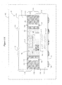
- FIGS. 6A-9B illustrate a substrate 601 comprising a multiplicity of subsystems each including a double embedded module of a type previously described.
- the substrate 601 will be described as a DSP subassembly substrate.
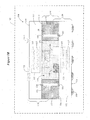
- FIGS. 7A and 7B illustrate a substrate 701 comprising a multiplicity of interconnect layer regions of a type previously described.
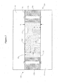
- FIGS. 8A and 8B illustrate a substrate 801 comprising a multiplicity of subsystems each including a module of a type previously described.
- the substrate 801 will be described as a radio subassembly substrate.
- FIGS. 6A-8B illustrate a multiplicity of SIP modules constructed from the substrates 601 , 701 , and 801 shown in FIGS. 6A-8B . It is understood that the subsystem substrates 601 and 801 can be fabricated to include modules other than DSP and radio modules (e.g., power management modules, NFMI modules, biometric sensor modules).
- modules other than DSP and radio modules e.g., power management modules, NFMI modules, biometric sensor modules.
- a flexible circuit substrate 602 is shown to include an arrangement (e.g., a matrix of rows and columns) of circuit regions 604 each containing a DSP subsystem 605 embedded into the flexible circuit substrate 602 preferably using WABE technology.
- the DSP subsystem 605 includes a double embedded DSP module 610 comprising one DSP die and one non-volatile memory die stacked above each other and embedded into the flexible circuit substrate 602 .
- the top surface of the flexible circuit substrate 602 includes solder pads to which SMT chip components 606 are placed using a pick-and-place technique.
- Each of the fully functional DSP modules 610 can be tested prior to additional fabrication processing. Defective DSP modules 610 can be identified and excluded from further processing.
- FIGS. 6A-8B show substrates 601 , 701 , 801 comprising nine circuit regions.
- each substrate 601 , 701 , 801 typically includes dozens or hundreds of circuit regions for fabricating a corresponding number of subsystems/SIP modules.
- the flexible circuit substrate 602 can be fabricated in approximately 50 mm ⁇ 150 mm strips with approximately 150 circuits per strip, depending on the actual circuit size.
- the top surface of the flexible circuit substrate 602 includes solder pads to which approximately 24 SMT chip components 606 are populated. Provided on the same surface of the flexible circuit substrate 602 and situated adjacent to the SMT component pads are several solder pads 608 .
- the solder pads 608 of the flexible circuit substrate 602 electrically connect with corresponding vertical interconnects 708 of the interconnect layer/substrate 701 when the interconnect substrate 701 is registered with, and bonded to, the flexible circuit substrate 602 .
- the vertical interconnect substrate 701 provides the required electrical routing paths to connect the DSP subsystems 605 with their corresponding radio subsystems 805 .
- the radio subassembly substrate 801 shown in FIGS. 8A and 8B includes a number of circuit regions 804 within which a 2.4 GHz radio module 805 is fabricated using flip-chip technology and a pick-and-place technique.
- a radio IC 810 is attached flip-chip style on a second surface 803 of the substrate 801 .
- solder pads 808 are also provided on the second surface 803 adjacent the radio IC 810 for establishing connections with the vertical interconnects 708 of the interconnect substrate 701 .
- a crystal oscillator, inductors, and capacitors 806 required for full radio functionality are mounted to the first surface 802 of the substrate 801 using SMT methods.
- Each of the fully functional radio subsystems 805 can be tested prior to additional fabrication processing. Defective radio subsystems 805 can be identified and excluded from further processing.
- the thickness of the vertical interconnect substrate 701 is selected to provide the thinnest possible package while maintaining adequate clearance between the radio die 810 of the radio subassembly substrate 801 and the passive components 606 attached to the flexible circuit substrate 602 of the DSP subassembly substrate 601 .
- An adhesive material can be used within the window 704 of the interconnect substrate 701 between the DSP subassembly substrate 601 and the radio subassembly substrate 801 .
- the adhesive material can serve as a mold compound and an adhesive to increase robustness of the SIP modules 904 .
- the adhesive can be applied in several fashions. For example, one approach is to use the adhesive as a semi-cured adhesive that is applied to the radio IC 810 at the wafer level. This semi-cured adhesive then flows during lamination or reflow and seals the space 704 between the DSP and radio subassembly substrates 601 and 801 .
- vertical interconnect pad connection material can be a WABE conductive paste or a lead-free solder paste. If a WABE conductive paste is used, an adhesive is pre-applied to the radio IC 810 and the radio IC components 806 are populated post-lamination to the first surface 802 of the substrate 801 . If solder is used, then the radio IC components 806 can be populated on the first surface 802 of the substrate 801 prior to assembly of the SIP modules 904 , and the adhesive material is dispensed post-SIP module assembly.
- a WABE conductive paste an adhesive is pre-applied to the radio IC 810 and the radio IC components 806 are populated post-lamination to the first surface 802 of the substrate 801 . If solder is used, then the radio IC components 806 can be populated on the first surface 802 of the substrate 801 prior to assembly of the SIP modules 904 , and the adhesive material is dispensed post-SIP module assembly.
- FIGS. 9A and 9B illustrate a multiplicity of fully functional SIP modules 904 constructed from the substrates 601 , 701 , and 801 shown in FIGS. 6A-8B .
- FIG. 9A shows saw lines (dashed lines) 906 superimposed over the SIP module composite substrate 901 . Individual SIP modules 904 are singulated by cutting through the saw lines. The singulated SIP modules 904 may then be incorporated into hearing assistance devices or other hearables.
- Item 1 is a hearing assistance device adapted for use in or on a wearer, the hearing assistance device comprising:
- SIP system in package
- Item 2 is the hearing assistance device of item 1, wherein the first substrate, the interconnect layer, and the second substrate define a vertically stacked structure.
- Item 3 is the hearing assistance device of item 1, wherein the window is sized to provide clearance for components supported on one or both of the second surfaces of the first and second substrates.
- Item 4 is the hearing assistance device of item 1, wherein each of the second surfaces supports one or more components.
- Item 5 is the hearing assistance device of item 1, wherein:
- one of the first surfaces supports one or more components
- the other of the first surfaces comprises a plurality of spaced-apart electrical contacts for communicating with and powering the SIP module.
- Item 6 is the hearing assistance device of item 1, wherein at least one of the first and second substrates comprises a flexible substrate.
- Item 7 is the hearing assistance device of item 1, wherein:
- the first substrate comprises a rigid substrate
- the second substrate comprises a flexible substrate.
- Item 8 is the hearing assistance device of item 1, wherein:
- the second substrate comprises a plurality of flexible substrate layers
- the second subsystem comprises a first integrated circuit (IC) and a second IC;
- the first and second ICs are separated by at least one of the flexible substrate layers.
- Item 9 is the hearing assistance device of item 8, wherein:
- the first subsystem comprises a communications device
- the first IC of the second subsystem comprises a processor IC
- the second IC of the second subsystem comprises a memory IC.
- Item 10 is the hearing assistance device of item 1, wherein:
- the first subsystem comprises a radio, a near-field magnetic induction (NFMI) device or one or more biometric sensors; and
- NFMI near-field magnetic induction
- the second subsystem comprises a processor integrated circuit (IC) or a power management IC.
- IC processor integrated circuit
- Item 11 is the hearing assistance device of item 1, wherein:
- the first subsystem comprises a 2.4 GHz radio
- the second subsystem comprises a processor integrated circuit (IC) embedded with a non-volatile memory IC.
- IC processor integrated circuit
- Item 12 is the hearing assistance device of item 1, wherein:
- the first subsystem is configured for functional testing prior to being connected to the second subsystem
- the second subsystem is configured for functional testing prior to being connected to the first subsystem.
- Item 13 is a hearing assistance device adapted for use in or on a wearer, the hearing assistance device comprising:
- SIP system in package
- DSP digital signal processor
- Item 14 is the hearing assistance device of item 13, wherein a non-volatile memory integrated circuit (IC) is embedded in the second substrate and electrically coupled to the DSP module.
- IC non-volatile memory integrated circuit
- Item 15 is the hearing assistance device of item 14, wherein at least one of the flexible layers separates the DSP module and the memory IC.
- Item 16 is the hearing assistance device of item 13, wherein:
- the first surface of the first substrate supports an antenna connection pad and one or more surface mount components coupled to the radio subsystem;
- the second surface of the second substrate supports one or more surface mount components coupled to the DSP module;
- the window of the interconnect layer is sized to accommodate the one or more surface mount components coupled to the radio subsystem and the one or more surface mount components coupled the DSP module;
- the first surface of the second substrate comprises a plurality of spaced-apart electrical contacts for communicating with and powering the SIP module.
- Item 17 is the hearing assistance device of item 13, wherein the radio subsystem comprises a 2.4 GHz radio integrated circuit.
- Item 18 is the hearing assistance device of item 13, wherein the first substrate, the interconnect layer, and the second substrate define a vertically stacked structure.
- Item 19 is the hearing assistance device of item 13, wherein the window is sized to provide clearance for components supported on one or both of the second surfaces of the first and second substrates.
- Item 20 is a hearing assistance device adapted for use in or on a wearer, the hearing assistance device comprising:
Landscapes
- Engineering & Computer Science (AREA)
- Health & Medical Sciences (AREA)
- General Health & Medical Sciences (AREA)
- Neurosurgery (AREA)
- Otolaryngology (AREA)
- Physics & Mathematics (AREA)
- Acoustics & Sound (AREA)
- Signal Processing (AREA)
- Computer Networks & Wireless Communication (AREA)
- Transceivers (AREA)
Abstract
Description
- This application relates generally to hearing assistance devices and methods of making such devices.
- Hearing aids are electronic instruments that compensate for hearing losses by amplifying sound. The electronic components of a hearing aid typically include a microphone for receiving ambient sound, an amplifier for amplifying the microphone signal, a speaker for converting the amplified microphone signal to sound for the wearer, and a battery for powering the components.
- Various embodiments are directed to a hearing assistance device adapted for use in or on a wearer. The hearing assistance device comprises an enclosure and a system in package (SIP) module disposed within the enclosure. The SIP module comprises a first substrate having a first surface and an opposing second surface. The first substrate supports a first subsystem configured to perform a first function. A second substrate having a first surface and an opposing second surface supports a second subsystem configured to perform a second function different from the first function. The second surfaces face each other and at least one of the second surfaces supports one or more components. An interconnect layer is separate from and bonded to and between the first and second substrates. The interconnect layer comprises a window and a region peripheral to the window. The window is sized to accommodate the one or more components and the peripheral region comprises electrical pathways for electrically connecting the first subsystem and the second subsystem.
- Some embodiments are directed to a hearing assistance device adapted for use in or on a wearer comprising an enclosure and an SIP module disposed within the enclosure. The SIP module comprises a radio subsystem and a digital signal processor (DSP) subsystem arranged in a vertically stacked configuration. The SIP module comprises a first substrate having a first surface and an opposing second surface. The second surface of the first substrate supports the radio subsystem. A second substrate comprises a plurality of flexible layers and has a first surface and an opposing second surface. At least a DSP module of the DSP subsystem is embedded in the second substrate. The second surfaces face each other. An interconnect layer is separate from and bonded to and between the first and second substrates. The interconnect layer comprises a window and a region peripheral to the window. The window is sized to accommodate at least the radio subsystem and the peripheral region comprising electrical pathways for electrically connecting the radio subsystem and the DSP subsystem.
- Other embodiments are directed to a hearing assistance device adapted for use in or on a wearer comprising an enclosure and a SIP module disposed within the enclosure. The SIP module comprises a first substrate having a first surface and an opposing second surface. The surface of the first substrate supports a radio subsystem. A second substrate comprises a plurality of flexible layers and has a first surface and an opposing second surface. A DSP subsystem is embedded in the second substrate. A non-volatile memory integrated circuit is embedded in the second substrate and separated from the DSP subsystem by at least one of the flexible layers. One or more surface mount components are coupled to the DSP subsystem and supported by the second surface of the second substrate. The second surfaces face each other. An interconnect layer is separate from and bonded to and between the first and second substrates. The interconnect layer comprises a window and a region peripheral to the window. The window is sized to accommodate the radio subsystem and the one or more surface mount components. The peripheral region comprises electrical pathways for electrically connecting the radio subsystem and the DSP subsystem.
- The above summary is not intended to describe each disclosed embodiment or every implementation of the present disclosure. The figures and the detailed description below more particularly exemplify illustrative embodiments.
- Throughout the specification reference is made to the appended drawings wherein:
-
FIG. 1A is a cross-sectional view of a SIP module comprising a multiplicity of subsystems for use in a hearing assistance device in accordance with various embodiments; -
FIG. 1B is a cross-sectional view of a SIP module comprising two double embedded subsystems for use in a hearing assistance device in accordance with various embodiments; -
FIG. 2 is a cross-sectional view showing details of a windowed interconnect layer of the SIP modules shown inFIGS. 1A and 1B in accordance with various embodiments; -
FIG. 3 is a cross-sectional view of a double embedded SIP module comprising a multiplicity of subsystems for use in a hearing assistance device in accordance with various embodiments; -
FIG. 4 illustrates details of the double embedded module shown inFIG. 3 in accordance with various embodiments; -
FIG. 5 illustrates a SIP module incorporated in a representative hearing assistance device in accordance with various embodiments; -
FIGS. 6A and 6B illustrate a substrate comprising a multiplicity of subsystems each including a double embedded module in accordance with various embodiments; -
FIGS. 7A and 7B illustrate a substrate comprising a multiplicity of interconnect layer regions in accordance with various embodiments; -
FIGS. 8A and 8B illustrate a substrate comprising a multiplicity of subsystems each including a module configured to perform one or more functions in accordance with various embodiments; and -
FIGS. 9A and 9B illustrate a multiplicity of SIP modules constructed from the substrates shown inFIGS. 6A-8B in accordance with various embodiments. - The figures are not necessarily to scale. Like numbers used in the figures refer to like components. However, it will be understood that the use of a number to refer to a component in a given figure is not intended to limit the component in another figure labeled with the same number.
- It is understood that the embodiments described herein may be used with any hearing device without departing from the scope of this disclosure. The devices depicted in the figures are intended to demonstrate the subject matter, but not in a limited, exhaustive, or exclusive sense. It is also understood that the present subject matter can be used with a device designed for use in or on the right ear or the left ear or both ears of the wearer.
- Hearing assistance devices, such as hearing aids and hearables (e.g., wearable earphones), typically include an enclosure, such as a housing or shell, within which internal components are disposed. Typical internal components of a hearing assistance device can include a signal processor, memory, power management circuitry, one or more communication devices, one or more antennas, one or more microphones, and a receiver/speaker, for example. The housing or shell of a hearing assistance device has a size limitation based on the application. Specifically, devices that include an in-the-ear shell or an on-the-ear shell are constrained by the geometry of the inner or outer ear of the wearer. More advanced hearing assistance devices can incorporate a long-range communication device, such as a Bluetooth® transceiver, space for which must be allocated within the shell of the device. As hearing assistance device technology continues to advance, a greater number of electronic components will be required to provide enhanced functionality, which further complicates the packaging strategy within the shell of the device.
- Embodiments of the disclosure are directed to a hearing assistance device which incorporates a multiplicity of electronic subsystems configured in the form of a system in package (SIP) module. The term SIP is often used interchangeably in industry with the term package-on-package (PoP). It is understood that the term SIP module as used herein also refers to a PoP module or a combined SIP/PoP module. According to various embodiments, a hearing assistance device incorporates a multiplicity of integrated circuits or chips arranged in multiple layers as a SIP module. For example, a multiplicity of integrated circuits or chips can be arranged in a vertically stacked configuration as a SIP module.
- Embodiments of the disclosure are directed to a SIP module adapted for use in various types of hearing devices, including hearables, hearing assistance devices, and/or hearing aids, including but not limited to, behind-the-ear (BTE), in-the-ear (ITE), in-the-canal (ITC), receiver-in-canal (RIC), receiver-in-the-ear (RITE) or completely-in-the-canal (CIC) type hearing devices. It is understood that behind-the-ear type hearing devices may include devices that reside substantially behind the ear or over the ear.
- According to various embodiments, a SIP module adapted for incorporation in a hearing assistance device includes at least two vertically stacked subsystems, each of which comprises at least one integrated circuit (IC). In some embodiments, the IC or ICs of one of the vertically stacked subsystems of the SIP module is/are embedded into a flexible circuit substrate. The IC or ICs of other vertically stacked subsystems of the SIP module can be supported by a rigid substrate or a flexible circuit substrate. In other embodiments, each of the vertically stacked subsystems can include one or more ICs embedded in a flexible circuit substrate.
- Embodiments of a SIP module incorporate an interconnect layer disposed between the vertically stacked subsystems. The interconnect layer comprises a discrete substrate having a window and a region peripheral to the window. The window of the interconnect layer is sized to accommodate one or more components mounted to or extending from internal surfaces of the vertically stacked subsystems. The peripheral region of the interconnect layer incorporates electrical pathways for electrically connecting the vertically stacked subsystems. Electrical contacts on an exterior surface or surfaces of the SIP module serve as input/output pads for establishing electrical connection with other components of the hearing assistance device, typically via a mother flexible circuit disposed within the shell.
- A SIP module that incorporates a multiplicity of vertically stacked subsystems each separated by a windowed interconnect layer provides for integration of a greater number of electronic components within the constrained space of an in- or on-the-ear hearing assistance device as compared to conventional packaging techniques. For example, a SIP module implemented in accordance with the present disclosure can accommodate four integrated circuits or dies within the space of two ICs or dies using conventional packaging techniques.
-
FIG. 1A is a cross-sectional view of a SIP module comprising a multiplicity of subsystems for use in a hearing assistance device in accordance with various embodiments.FIG. 1A shows aSIP module 104 incorporated within ahearing assistance device 102. TheSIP module 104 includes afirst subsystem 110 and asecond subsystem 130. Thefirst subsystem 110 is a fully functional system that performs a first function, and thesecond subsystem 130 is a fully functional system that performs a second function. The first function performed by thefirst subsystem 110 is preferably different from the second function performed by thesecond subsystem 130. The first function, for example, may be a communication function, and the second function may be a signal processing function or a power management function. Other functions performed by the first andsecond subsystems - In the embodiment shown in
FIG. 1A , thefirst subsystem 110 includes afirst substrate 112 having afirst surface 114 and an opposingsecond surface 116. Thefirst substrate 112 can be a rigid substrate or a flexible substrate with layers that interconnect via electrically conductive pathways or traces. For example, thefirst substrate 112 can be a printed circuit board (PCB) formed from a rigid material such as bismaleimide-triazine (BT) resin, FR4 (e.g., glass-reinforced epoxy laminate) or other type of rigid PCB material. - The
first surface 114 of thefirst substrate 112 supports one ormore components components first surface 114 for illustrative purposes, it is understood that any number of components may be supported by thefirst surface 114 of thefirst substrate 112. Thesecond surface 116 of thefirst substrate 112 supports one ormore components 120. The one ormore components 120 can include an SMT component, a flip-chip, a chip scale package-on-board (CSPOB) module, or a mix of these components/modules. - The
second subsystem 130 includes asecond substrate 132 having afirst surface 134 and an opposingsecond surface 136. In the vertically stacked structure shown inFIG. 1A , thesecond surface 136 of thesecond substrate 132 faces (e.g., is substantially parallel to) thesecond surface 116 of thefirst substrate 112 in a spaced-apart relationship. Thesecond surface 136 of thesecond substrate 132 supports one ormore components 138 and 140 (two components are shown for illustrative purposes), which may include any mix of SMT components, a flip-chip, and a CSPOB module. According to various embodiments, thesecond substrate 132 constitutes a flexible circuit substrate into which one or more components are embedded. The flexible circuit substrate may be constructed from films of a polyimide material. In some embodiments, thesecond substrate 132 constitutes a flexible circuit board into which severalintegrated chips module 133 are embedded vertically to define a wafer and board level device embedded package or WABE. - The
first surface 134 of thesecond substrate 132 includes a multiplicity ofelectrical contacts 180. Theelectrical contacts 180 serve as user input/output (I/O) pads for theSIP module 104. For example, theelectrical contacts 180 connect theSIP module 104 with other components of thehearing assistance device 102, such as a battery, microphones, receiver, transceiver, and other components. Theelectrical contacts 180 may constitute electrically conductive traces, solder bumps or balls (e.g., a ball grid array or BGA), or other type of electrical contact. For example, theelectrical contacts 180 may be configured to allow for either BGA style gang reflow onto a mother flex circuit (see, e.g.,FIG. 5 ) or individual hand wire soldering methods. - The first and
second subsystems subsystem interconnect layer 150 is disposed between the first andsecond subsystems interconnect layer 150 is a discrete layer that separates the first andsecond subsystems interconnect layer 150 can constitute a substrate formed from a rigid material such as BT resin or FR4. In some embodiments theinterconnect layer 150 can constitute a flexible substrate, such as one formed from polyimide or another suitable flexible substrate material. Theinterconnect layer 150 includes a window 170 (e.g., an aperture or void) and asolid region 172 peripheral to thewindow 170. Thewindow 170 is sized to accommodate thecomponents second surfaces second substrates window 170 is preferably filled withfiller material 171, such as an adhesive. - The
window 170 is shown as a void in the shape of a square or a rectangle inFIG. 1A and other figures for purposes of illustration. It is understood that thewindow 170 can have a different shape, such as a curved shape, and need not be centrally located within theinterconnect layer 150. Moreover, thewindow 170 need not be a single window, but may include a multiplicity of apertures or voids that accommodate individual components or groups of components. Additional details concerning theinterconnect layer 150 are disclosed in commonly owned U.S. Pat. No. 5,825,631, which is incorporated herein by reference. - Referring now to
FIG. 2 , the vertical height of thewindow 170 of theinterconnect layer 150 is sized to accommodate the vertical height of the various electronic components populating the opposingsecond surfaces second substrates window 170 is shown as height h1, which corresponds to the thickness of theinterconnect layer 150. In general, the thickness of theinterconnect layer 150 is selected to provide the thinnest possible package while maintaining adequate clearance between the electronic and electrical components attached to the opposingsecond surfaces second substrates window 170 is sized to provide clearance for electronic components populating the opposingsecond surfaces second substrates - The largest component 120 (in terms of height) supported by the
second surface 116 of thefirst substrate 112 has a height of h2. The largest component 140 (in terms of height) supported by thesecond surface 136 of thesecond substrate 132 has a height of h3. In general, the height, h1, of thewindow 170 is preferably equal to or greater than the combined height, h2+h3, of thelargest components second surfaces second surfaces window 170 can be less than the combined height, h2+h3, of thelargest components largest components window 170 to be less than the combined height, h2+h3, of thelargest components - Returning to
FIG. 1A , theperipheral region 172 of theinterconnect layer 150 includeselectrical pathways first subsystem 110 and thesecond subsystem 130. Theelectrical pathways peripheral region 172 and terminate atinterconnect pads vertical interconnects second subsystems vertical interconnects FIG. 1A (and other figures). It is understood that more than two vertical interconnects can be incorporated in the cross-section of theperipheral region 172 shown inFIG. 1A . Thevertical interconnects FIG. 1A and other figures, the conductive traces that provide electrical connection between the various components and thesubsystems SIP module 104 are implicit in the figures, and are omitted for purposes of clarity. -
FIG. 1B is a cross-sectional view of a SIP module comprising two double embedded subsystems for use in a hearing assistance device in accordance with various embodiments. TheSIP module 104 shown inFIG. 1B is similar to that shown inFIG. 1A , but incorporates two double embeddedmodules second subsystems module 113 includes twointegrated circuits module 133 includes twointegrated circuits integrated circuits -
FIG. 3 is a cross-sectional view of a SIP module comprising a multiplicity of subsystems for use in a hearing assistance device in accordance with various embodiments. TheSIP module 104 shown inFIG. 3 includes afirst subsystem 110 electrically coupled to asecond subsystem 130 via a multiplicity ofvertical interconnects interconnect layer 150 disposed between the first andsecond subsystems first subsystem 110 constitutes a communication subsystem, and thesecond subsystem 130 constitutes a DSP (digital signal processing) subsystem. In other embodiments, thefirst subsystem 110 constitutes a communication subsystem, and thesecond subsystem 130 constitutes a power management subsystem. In further embodiments, thefirst subsystem 110 constitutes a biometric sensor subsystem, and thesecond subsystem 130 constitutes a processor-based subsystem. It is understood that the functions performed by the first andsecond subsystems - In the following discussion, the
first subsystem 110 is described as a communication subsystem and thesecond subsystem 130 is described as a DSP subsystem. Thecommunication subsystem 110 comprises afirst substrate 112 having afirst surface 114 and an opposingsecond surface 116. Thefirst surface 114 of thefirst substrate 112 supportsvarious SMT components 124 and 126 (two components are shown for illustrative purposes) and anantenna connection pad 122. Thesecond surface 116 of thefirst substrate 112 supports acommunication device 120, which is preferably packaged in the form of a flip-chip or a CSPOB module. According to some embodiments, thecommunication device 120 comprises a 2.4 GHz radio subsystem packaged as a flip-chip or a CSPOB module. A suitable radio subsystem is a 2.4 GHz Bluetooth® Low Energy (BLE) radio subsystem. Therepresentative SMT components FIG. 3 represent a crystal oscillator, inductors, capacitors, and other components required for full radio functionality. Thecommunication device 120 can be attached to traces on thesecond surface 116 of thefirst substrate 112 flip-chip style via solder bumps 121. In some embodiments, thecommunication device 120 comprises a 900 MHz radio subsystem. In other embodiments, thecommunication device 120 comprises a near-field magnetic induction (NFMI) device. In further embodiments, thecommunication device 120 can be substituted for a sensor, such as a physiologic, motion, light, temperature, moisture or magnetic sensor, for example. Useful biometric sensors can include one or more of an oxygen saturation sensor (e.g., pulse oximeter or plethysmography sensor), a heart rate sensor, and an electroencephalogram sensor, for example. - According to various embodiments, the
second subsystem 130 includes aflexible circuit substrate 132 which supports a double embeddedDSP module 133 comprising aDSP IC 137 and anon-volatile memory IC 135. Although not shown, conductive traces electrically connect theDSP IC 137 and thememory IC 135. TheDSP IC 137 and thememory IC 135 are both embedded into theflexible circuit substrate 132, one directly atop the other, preferably in the form of a WABE module. In accordance with other embodiments, thesecond subsystem 130 can include a double embedded module with ICs that provide different functionality. For example, the double embeddedmodule 133 can include an analog ASIC 135 (primarily analog but may include some digital elements) and a digital ASIC 137 (primarily digital but may include some analog elements). In further embodiments, themodule 133 may be a double embedded or a single embedded module which includes a power management IC. - An
interconnect layer 150 is disposed between thecommunication subsystem 110 and theDSP subsystem 130. Theinterconnect layer 150 is of a form and construction previously described. Thewindow 170 of theinterconnect layer 150 is sized to accommodate the communication device 120 (e.g., radio IC) and thepassive SMT components DSP module 133. The thickness of theinterconnect layer 150 is selected to provide the thinnest possible package while maintaining adequate clearance between thecommunication device 120 and thepassive SMT components -
FIG. 4 illustrates details of the double embeddedmodule 133 shown inFIG. 3 in accordance with various embodiments. In the embodiment shown inFIG. 4 , theflexible circuit substrate 132 includes a multiplicity of flexible films within which twoICs ICs IC 135 can be a non-volatile memory IC, andIC 137 can be a DSP IC. - The
first IC 135 is disposed betweenorganic layers first IC 135 embedded within aflexible core film 404. Thefirst IC 135 includes solder bumps 141 that connect with corresponding traces (not shown) of theorganic layer 406. Thesecond IC 137 is disposed betweenorganic layers second IC 137 embedded within aflexible core film 408. Thesecond IC 137 includes solder bumps 143 that connect with corresponding traces (not shown) of theorganic layer 410. One or more additionalflexible layers 412 may be provided adjacent theorganic layer 410 to rigidize theflexible substrate 132. It is noted that one or more additional flexible layers can be provided adjacent theorganic layer 402 to further rigidize theflexible substrate 132. - According to some embodiments, the
flexible layers flexible layers ICs -
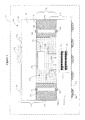
FIG. 5 illustrates aSIP module 104 incorporated in a representativehearing assistance device 102 in accordance with various embodiments. Thehearing assistance device 102 shown inFIG. 5 includes aSIP module 104 of a type previously described. TheSIP module 104 is electrically connected to a motherflexible circuit 502 to which other components of thehearing assistance device 102 are electrically connected. Abattery 504 is electrically connected to the motherflexible circuit 502 and provides power to the various components of thehearing assistance device 102. One or more microphones 506 are electrically connected to the motherflexible circuit 502, which provides electrical communication between the microphones 506 and theSIP module 104. One or more user switches 508 (e.g., on/off, volume, mic directional settings) are electrically coupled to theSIP module 104 via theflexible mother circuit 502. - An
audio output device 510 is electrically connected to theSIP module 104 via theflexible mother circuit 502. In some embodiments, theaudio output device 510 comprises a speaker (coupled to an amplifier). In other embodiments, theaudio output device 510 comprises an amplifier coupled to anexternal receiver 512 adapted for positioning within an ear of a user. Thehearing assistance device 102 may incorporate acommunication device 507 coupled to theflexible mother circuit 502 and to anantenna 509 directly or indirectly via theflexible mother circuit 502. Thecommunication device 507 can be a Bluetooth® transceiver, such as a BLE (Bluetooth® low energy) transceiver or other transceiver (e.g., an IEEE 802.11 compliant device). It is noted that, in some embodiments, one or both of thecommunication device 507 and theaudio output device 510 can be incorporated in theSIP module 104. - A SIP module implemented in accordance with various embodiments of the disclosure includes a fully functional first subsystem, a fully functional second subsystem, and an interconnect layer disposed between the first and second subsystems. During SIP module fabrication, the three-part SIP module configuration advantageously allows for individual testing of the first and second subsystems prior to constructing the SIP modules. Individual testing of the first and second subsystems allows for identification of defective subsystems prior to constructing the SIP modules, which avoids wasteful discarding of a properly operating subsystem if integrated with a defective subsystem.
- Methods of fabricating a SIP module in accordance with various embodiments will now be described with reference to
FIGS. 6A-9B .FIGS. 6A and 6B illustrate asubstrate 601 comprising a multiplicity of subsystems each including a double embedded module of a type previously described. For purposes of illustration, thesubstrate 601 will be described as a DSP subassembly substrate.FIGS. 7A and 7B illustrate asubstrate 701 comprising a multiplicity of interconnect layer regions of a type previously described.FIGS. 8A and 8B illustrate asubstrate 801 comprising a multiplicity of subsystems each including a module of a type previously described. For purposes of illustration, thesubstrate 801 will be described as a radio subassembly substrate.FIGS. 9A and 9B illustrate a multiplicity of SIP modules constructed from thesubstrates FIGS. 6A-8B . It is understood that thesubsystem substrates - According to various embodiments, and with reference to
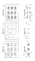
FIGS. 6A and 6B , aflexible circuit substrate 602 is shown to include an arrangement (e.g., a matrix of rows and columns) ofcircuit regions 604 each containing aDSP subsystem 605 embedded into theflexible circuit substrate 602 preferably using WABE technology. TheDSP subsystem 605 includes a double embeddedDSP module 610 comprising one DSP die and one non-volatile memory die stacked above each other and embedded into theflexible circuit substrate 602. The top surface of theflexible circuit substrate 602 includes solder pads to whichSMT chip components 606 are placed using a pick-and-place technique. Each of the fullyfunctional DSP modules 610 can be tested prior to additional fabrication processing.Defective DSP modules 610 can be identified and excluded from further processing. - For purposes of simplicity,
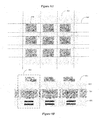
FIGS. 6A- 8B show substrates substrate flexible circuit substrate 602 can be fabricated in approximately 50 mm×150 mm strips with approximately 150 circuits per strip, depending on the actual circuit size. The top surface of theflexible circuit substrate 602 includes solder pads to which approximately 24SMT chip components 606 are populated. Provided on the same surface of theflexible circuit substrate 602 and situated adjacent to the SMT component pads areseveral solder pads 608. Thesolder pads 608 of theflexible circuit substrate 602 electrically connect with correspondingvertical interconnects 708 of the interconnect layer/substrate 701 when theinterconnect substrate 701 is registered with, and bonded to, theflexible circuit substrate 602. As was discussed previously, thevertical interconnect substrate 701 provides the required electrical routing paths to connect theDSP subsystems 605 with theircorresponding radio subsystems 805. - The
radio subassembly substrate 801 shown inFIGS. 8A and 8B includes a number ofcircuit regions 804 within which a 2.4GHz radio module 805 is fabricated using flip-chip technology and a pick-and-place technique. As is shown inFIG. 8B , aradio IC 810 is attached flip-chip style on asecond surface 803 of thesubstrate 801. Also provided on thesecond surface 803 adjacent theradio IC 810 aresolder pads 808 for establishing connections with thevertical interconnects 708 of theinterconnect substrate 701. A crystal oscillator, inductors, andcapacitors 806 required for full radio functionality are mounted to thefirst surface 802 of thesubstrate 801 using SMT methods. Each of the fullyfunctional radio subsystems 805 can be tested prior to additional fabrication processing.Defective radio subsystems 805 can be identified and excluded from further processing. - As was previously discussed, the thickness of the
vertical interconnect substrate 701 is selected to provide the thinnest possible package while maintaining adequate clearance between the radio die 810 of theradio subassembly substrate 801 and thepassive components 606 attached to theflexible circuit substrate 602 of theDSP subassembly substrate 601. An adhesive material can be used within thewindow 704 of theinterconnect substrate 701 between theDSP subassembly substrate 601 and theradio subassembly substrate 801. The adhesive material can serve as a mold compound and an adhesive to increase robustness of theSIP modules 904. The adhesive can be applied in several fashions. For example, one approach is to use the adhesive as a semi-cured adhesive that is applied to theradio IC 810 at the wafer level. This semi-cured adhesive then flows during lamination or reflow and seals thespace 704 between the DSP andradio subassembly substrates - It is noted that vertical interconnect pad connection material can be a WABE conductive paste or a lead-free solder paste. If a WABE conductive paste is used, an adhesive is pre-applied to the
radio IC 810 and theradio IC components 806 are populated post-lamination to thefirst surface 802 of thesubstrate 801. If solder is used, then theradio IC components 806 can be populated on thefirst surface 802 of thesubstrate 801 prior to assembly of theSIP modules 904, and the adhesive material is dispensed post-SIP module assembly. -
FIGS. 9A and 9B illustrate a multiplicity of fullyfunctional SIP modules 904 constructed from thesubstrates FIGS. 6A-8B .FIG. 9A shows saw lines (dashed lines) 906 superimposed over the SIP modulecomposite substrate 901.Individual SIP modules 904 are singulated by cutting through the saw lines. Thesingulated SIP modules 904 may then be incorporated into hearing assistance devices or other hearables. - This document discloses numerous embodiments, including but not limited to the following:
-
Item 1 is a hearing assistance device adapted for use in or on a wearer, the hearing assistance device comprising: - an enclosure; and
- a system in package (SIP) module disposed within the enclosure, the SIP module comprising:
-
- a first substrate having a first surface and an opposing second surface, the first substrate supporting a first subsystem configured to perform a first function;
- a second substrate having a first surface and an opposing second surface, the second substrate supporting a second subsystem configured to perform a second function different from the first function;
- the second surfaces facing each other and at least one of the second surfaces supporting one or more components; and
- an interconnect layer separate from and bonded to and between the first and second substrates, the interconnect layer comprising a window and a region peripheral to the window, the window sized to accommodate the one or more components and the peripheral region comprising electrical pathways for electrically connecting the first subsystem and the second subsystem.
-
Item 2 is the hearing assistance device ofitem 1, wherein the first substrate, the interconnect layer, and the second substrate define a vertically stacked structure. - Item 3 is the hearing assistance device of
item 1, wherein the window is sized to provide clearance for components supported on one or both of the second surfaces of the first and second substrates. - Item 4 is the hearing assistance device of
item 1, wherein each of the second surfaces supports one or more components. - Item 5 is the hearing assistance device of
item 1, wherein: - one of the first surfaces supports one or more components; and
- the other of the first surfaces comprises a plurality of spaced-apart electrical contacts for communicating with and powering the SIP module.
-
Item 6 is the hearing assistance device ofitem 1, wherein at least one of the first and second substrates comprises a flexible substrate. -
Item 7 is the hearing assistance device ofitem 1, wherein: - the first substrate comprises a rigid substrate; and
- the second substrate comprises a flexible substrate.
- Item 8 is the hearing assistance device of
item 1, wherein: - the second substrate comprises a plurality of flexible substrate layers;
- the second subsystem comprises a first integrated circuit (IC) and a second IC; and
- the first and second ICs are separated by at least one of the flexible substrate layers.
- Item 9 is the hearing assistance device of item 8, wherein:
- the first subsystem comprises a communications device;
- the first IC of the second subsystem comprises a processor IC; and
- the second IC of the second subsystem comprises a memory IC.
- Item 10 is the hearing assistance device of
item 1, wherein: - the first subsystem comprises a radio, a near-field magnetic induction (NFMI) device or one or more biometric sensors; and
- the second subsystem comprises a processor integrated circuit (IC) or a power management IC.
- Item 11 is the hearing assistance device of
item 1, wherein: - the first subsystem comprises a 2.4 GHz radio; and
- the second subsystem comprises a processor integrated circuit (IC) embedded with a non-volatile memory IC.
- Item 12 is the hearing assistance device of
item 1, wherein: - the first subsystem is configured for functional testing prior to being connected to the second subsystem; and
- the second subsystem is configured for functional testing prior to being connected to the first subsystem.
- Item 13 is a hearing assistance device adapted for use in or on a wearer, the hearing assistance device comprising:
- an enclosure; and
- a system in package (SIP) module disposed within the enclosure and comprising a radio subsystem and a digital signal processor (DSP) subsystem arranged in a vertically stacked configuration, the SIP module comprising:
-
- a first substrate having a first surface and an opposing second surface, the second surface of the first substrate supporting the radio subsystem;
- a second substrate comprising a plurality of flexible layers and having a first surface and an opposing second surface, wherein at least a DSP module of the DSP subsystem is embedded in the second substrate;
- the second surfaces facing each other; and
- an interconnect layer separate from and bonded to and between the first and second substrates, the interconnect layer comprising a window and a region peripheral to the window, the window sized to accommodate at least the radio subsystem and the peripheral region comprising electrical pathways for electrically connecting the radio subsystem and the DSP subsystem.
- Item 14 is the hearing assistance device of item 13, wherein a non-volatile memory integrated circuit (IC) is embedded in the second substrate and electrically coupled to the DSP module.
- Item 15 is the hearing assistance device of item 14, wherein at least one of the flexible layers separates the DSP module and the memory IC.
- Item 16 is the hearing assistance device of item 13, wherein:
- the first surface of the first substrate supports an antenna connection pad and one or more surface mount components coupled to the radio subsystem;
- the second surface of the second substrate supports one or more surface mount components coupled to the DSP module;
- the window of the interconnect layer is sized to accommodate the one or more surface mount components coupled to the radio subsystem and the one or more surface mount components coupled the DSP module; and
- the first surface of the second substrate comprises a plurality of spaced-apart electrical contacts for communicating with and powering the SIP module.
- Item 17 is the hearing assistance device of item 13, wherein the radio subsystem comprises a 2.4 GHz radio integrated circuit.
- Item 18 is the hearing assistance device of item 13, wherein the first substrate, the interconnect layer, and the second substrate define a vertically stacked structure.
-
Item 19 is the hearing assistance device of item 13, wherein the window is sized to provide clearance for components supported on one or both of the second surfaces of the first and second substrates. - Item 20 is a hearing assistance device adapted for use in or on a wearer, the hearing assistance device comprising:
- an enclosure; and
- a system in package (SIP) module disposed within the enclosure, the SIP module comprising:
-
- a first substrate having a first surface and an opposing second surface, the second surface of the first substrate supporting a radio subsystem;
- a second substrate comprising a plurality of flexible layers and having a first surface and an opposing second surface;
- a digital signal processor (DSP) subsystem embedded in the second substrate;
- a non-volatile memory integrated circuit (IC) embedded in the second substrate and separated from the DSP subsystem by at least one of the flexible layers;
- one or more surface mount components coupled to the DSP subsystem and supported by the second surface of the second substrate;
- the second surfaces facing each other; and
- an interconnect layer separate from and bonded to and between the first and second substrates, the interconnect layer comprising a window and a region peripheral to the window, the window sized to accommodate the radio subsystem and the one or more surface mount components, and the peripheral region comprising electrical pathways for electrically connecting the radio subsystem and the DSP subsystem.
- Although the subject matter has been described in language specific to structural features and/or methodological acts, it is to be understood that the subject matter defined in the appended claims is not necessarily limited to the specific features or acts described above. Rather, the specific features and acts described above are disclosed as representative forms of implementing the claims.
Claims (20)
Priority Applications (2)
| Application Number | Priority Date | Filing Date | Title |
|---|---|---|---|
| US15/285,299 US10085097B2 (en) | 2016-10-04 | 2016-10-04 | Hearing assistance device incorporating system in package module |
| US16/108,440 US10582319B2 (en) | 2016-10-04 | 2018-08-22 | Hearing assistance device incorporating system in package module |
Applications Claiming Priority (1)
| Application Number | Priority Date | Filing Date | Title |
|---|---|---|---|
| US15/285,299 US10085097B2 (en) | 2016-10-04 | 2016-10-04 | Hearing assistance device incorporating system in package module |
Related Child Applications (1)
| Application Number | Title | Priority Date | Filing Date |
|---|---|---|---|
| US16/108,440 Continuation US10582319B2 (en) | 2016-10-04 | 2018-08-22 | Hearing assistance device incorporating system in package module |
Publications (2)
| Publication Number | Publication Date |
|---|---|
| US20180098162A1 true US20180098162A1 (en) | 2018-04-05 |
| US10085097B2 US10085097B2 (en) | 2018-09-25 |
Family
ID=61758657
Family Applications (2)
| Application Number | Title | Priority Date | Filing Date |
|---|---|---|---|
| US15/285,299 Active US10085097B2 (en) | 2016-10-04 | 2016-10-04 | Hearing assistance device incorporating system in package module |
| US16/108,440 Active US10582319B2 (en) | 2016-10-04 | 2018-08-22 | Hearing assistance device incorporating system in package module |
Family Applications After (1)
| Application Number | Title | Priority Date | Filing Date |
|---|---|---|---|
| US16/108,440 Active US10582319B2 (en) | 2016-10-04 | 2018-08-22 | Hearing assistance device incorporating system in package module |
Country Status (1)
| Country | Link |
|---|---|
| US (2) | US10085097B2 (en) |
Cited By (5)
| Publication number | Priority date | Publication date | Assignee | Title |
|---|---|---|---|---|
| US20170156011A1 (en) * | 2015-12-01 | 2017-06-01 | Gn Resound A/S | Hearing aid with a flexible carrier antenna and related method |
| US10085097B2 (en) * | 2016-10-04 | 2018-09-25 | Starkey Laboratories, Inc. | Hearing assistance device incorporating system in package module |
| US20190050573A1 (en) * | 2018-10-17 | 2019-02-14 | Intel Corporation | Secure boot processor with embedded nvram |
| US11252519B2 (en) * | 2018-11-30 | 2022-02-15 | Gn Hearing A/S | Hearing device with embedded integrated circuit chips |
| CN114208398A (en) * | 2019-06-18 | 2022-03-18 | 大北欧听力公司 | Printed Circuit Board (PCB) module including embedded radio frequency semiconductor die |
Citations (5)
| Publication number | Priority date | Publication date | Assignee | Title |
|---|---|---|---|---|
| US20040141627A1 (en) * | 2000-02-23 | 2004-07-22 | Hei, Inc. | Hearing-aid assembly using folded flex circuits |
| US6771786B1 (en) * | 1999-07-28 | 2004-08-03 | Oticon A/S | Hearing aid including an integrated circuit |
| US7279795B2 (en) * | 2005-12-29 | 2007-10-09 | Intel Corporation | Stacked die semiconductor package |
| US20080192967A1 (en) * | 2007-02-06 | 2008-08-14 | Chor Fan Chan | Circuit arrangement with bonded SMD component |
| US9695040B2 (en) * | 2012-10-16 | 2017-07-04 | Invensense, Inc. | Microphone system with integrated passive device die |
Family Cites Families (51)
| Publication number | Priority date | Publication date | Assignee | Title |
|---|---|---|---|---|
| US5825631A (en) | 1997-04-16 | 1998-10-20 | Starkey Laboratories | Method for connecting two substrates in a thick film hybrid circuit |
| CA2218307C (en) | 1997-10-10 | 2006-01-03 | Gennum Corporation | Three dimensional packaging configuration for multi-chip module assembly |
| US6724902B1 (en) * | 1999-04-29 | 2004-04-20 | Insound Medical, Inc. | Canal hearing device with tubular insert |
| US6456720B1 (en) * | 1999-12-10 | 2002-09-24 | Sonic Innovations | Flexible circuit board assembly for a hearing aid |
| US6532295B1 (en) * | 1999-12-10 | 2003-03-11 | Sonic Innovations, Inc. | Method for fitting a universal hearing device shell and conformal tip in an ear canal |
| DE10015421C2 (en) * | 2000-03-28 | 2002-07-04 | Implex Ag Hearing Technology I | Partially or fully implantable hearing system |
| DE10018334C1 (en) * | 2000-04-13 | 2002-02-28 | Implex Hear Tech Ag | At least partially implantable system for the rehabilitation of a hearing impairment |
| DE10114838A1 (en) * | 2001-03-26 | 2002-10-10 | Implex Ag Hearing Technology I | Fully implantable hearing system |
| US6956268B2 (en) * | 2001-05-18 | 2005-10-18 | Reveo, Inc. | MEMS and method of manufacturing MEMS |
| US7127078B2 (en) * | 2001-10-03 | 2006-10-24 | Advanced Bionics Corporation | Implanted outer ear canal hearing aid |
| ATE404033T1 (en) * | 2005-01-17 | 2008-08-15 | Widex As | DEVICE AND METHOD FOR OPERATING A HEARING AID |
| WO2006091808A2 (en) * | 2005-02-25 | 2006-08-31 | Medical Research Products-B, Inc. | Fully implantable hearing aid system |
| WO2006138289A2 (en) | 2005-06-14 | 2006-12-28 | United States Gypsum Company | Gypsum products utilizing a two-repeating unit dispersant and a method for making them |
| US7202552B2 (en) * | 2005-07-15 | 2007-04-10 | Silicon Matrix Pte. Ltd. | MEMS package using flexible substrates, and method thereof |
| KR20090033451A (en) * | 2006-06-30 | 2009-04-03 | 사임베트 코퍼레이션 | Thin Film Battery Recharge System and Method |
| JP2010534381A (en) * | 2007-03-05 | 2010-11-04 | コーニンクレッカ フィリップス エレクトロニクス エヌ ヴィ | Electrochemical energy source and electronic device with such electrochemical energy source |
| EP2135311A2 (en) * | 2007-04-02 | 2009-12-23 | Koninklijke Philips Electronics N.V. | Electrochemical energy source and electronic device provided with such an electrochemical energy source |
| US7923830B2 (en) | 2007-04-13 | 2011-04-12 | Maxim Integrated Products, Inc. | Package-on-package secure module having anti-tamper mesh in the substrate of the upper package |
| TW200919803A (en) * | 2007-06-07 | 2009-05-01 | Koninkl Philips Electronics Nv | Solid-state battery and method for manufacturing of such a solid-state battery |
| US8952511B2 (en) * | 2007-12-18 | 2015-02-10 | Intel Corporation | Integrated circuit package having bottom-side stiffener |
| US20120212904A1 (en) * | 2008-02-12 | 2012-08-23 | Robert Fleming | Flexible circuits and substrates comprising voltage switchable dielectric material |
| JP2010004513A (en) * | 2008-05-19 | 2010-01-07 | Yamaha Corp | Ear phone |
| US7842542B2 (en) | 2008-07-14 | 2010-11-30 | Stats Chippac, Ltd. | Embedded semiconductor die package and method of making the same using metal frame carrier |
| AU2009271129B2 (en) * | 2008-07-14 | 2013-10-10 | Otonomy, Inc. | Controlled-release apoptosis modulating compositions and methods for the treatment of otic disorders |
| CA2639555A1 (en) | 2008-08-11 | 2008-12-15 | Hyman Ngo | High definition litho applique and emblems |
| US8369553B2 (en) | 2008-12-19 | 2013-02-05 | Starkey Laboratories, Inc. | Hearing assistance device with stacked die |
| US8737658B2 (en) * | 2008-12-19 | 2014-05-27 | Starkey Laboratories, Inc. | Three dimensional substrate for hearing assistance devices |
| US8224006B2 (en) * | 2009-08-28 | 2012-07-17 | Siemens Medical Instruments Pte. Ltd. | Hearing aid device and a method of manufacturing a hearing aid device |
| KR20110074135A (en) | 2009-12-24 | 2011-06-30 | 삼성전자주식회사 | System-in-package with embedded circuit board |
| KR101612851B1 (en) * | 2010-02-01 | 2016-04-18 | 삼성전자주식회사 | Small hearing aid |
| KR20120079742A (en) | 2011-01-05 | 2012-07-13 | 삼성전자주식회사 | Folded stacked package and method for manufacturing the same |
| CN103416075B (en) * | 2011-03-07 | 2017-07-04 | 声奇股份公司 | Audio frequency apparatus |
| US20120267782A1 (en) * | 2011-04-25 | 2012-10-25 | Yung-Hsiang Chen | Package-on-package semiconductor device |
| US8247269B1 (en) | 2011-06-29 | 2012-08-21 | Fairchild Semiconductor Corporation | Wafer level embedded and stacked die power system-in-package packages |
| US9144490B2 (en) * | 2012-04-30 | 2015-09-29 | California Institute Of Technology | High-lead count implant device and method of making the same |
| US10008443B2 (en) * | 2012-04-30 | 2018-06-26 | California Institute Of Technology | Implant device |
| US9041205B2 (en) * | 2013-06-28 | 2015-05-26 | Intel Corporation | Reliable microstrip routing for electronics components |
| US9913052B2 (en) | 2013-11-27 | 2018-03-06 | Starkey Laboratories, Inc. | Solderless hearing assistance device assembly and method |
| US9906879B2 (en) | 2013-11-27 | 2018-02-27 | Starkey Laboratories, Inc. | Solderless module connector for a hearing assistance device assembly |
| US10425724B2 (en) * | 2014-03-13 | 2019-09-24 | Starkey Laboratories, Inc. | Interposer stack inside a substrate for a hearing assistance device |
| US9474154B2 (en) | 2014-07-18 | 2016-10-18 | Starkey Laboratories, Inc. | Reflow solderable flexible circuit board — to — flexible circuit board connector reinforcement |
| WO2016044178A1 (en) * | 2014-09-15 | 2016-03-24 | iHear Medical, Inc. | Canal hearing device with elongate frequency shaping sound channel |
| US9832860B2 (en) * | 2014-09-26 | 2017-11-28 | Intel Corporation | Panel level fabrication of package substrates with integrated stiffeners |
| CN107079226A (en) * | 2014-10-09 | 2017-08-18 | 索诺亚公司 | Auditory prosthesis |
| US20160268213A1 (en) * | 2015-03-09 | 2016-09-15 | Intel Corporation | On Package Floating Metal/Stiffener Grounding to Mitigate RFI and SI Risks |
| US9527721B2 (en) * | 2015-05-15 | 2016-12-27 | Taiwan Semiconductor Manufacturing Co., Ltd. | Movement microelectromechanical systems (MEMS) package |
| US10887706B2 (en) * | 2015-06-29 | 2021-01-05 | Hear-Wear Technologies LLC | Transducer modules for auditory communication devices and auditory communication devices |
| TW201709025A (en) * | 2015-08-26 | 2017-03-01 | 巨擘科技股份有限公司 | Device for integrating position, gesture, and wireless transmission |
| US20170178994A1 (en) * | 2015-12-21 | 2017-06-22 | Intel Corporation | Integrated circuit package support structures |
| US10741486B2 (en) * | 2016-03-06 | 2020-08-11 | Intel Corporation | Electronic components having three-dimensional capacitors in a metallization stack |
| US10085097B2 (en) * | 2016-10-04 | 2018-09-25 | Starkey Laboratories, Inc. | Hearing assistance device incorporating system in package module |
-
2016
- 2016-10-04 US US15/285,299 patent/US10085097B2/en active Active
-
2018
- 2018-08-22 US US16/108,440 patent/US10582319B2/en active Active
Patent Citations (5)
| Publication number | Priority date | Publication date | Assignee | Title |
|---|---|---|---|---|
| US6771786B1 (en) * | 1999-07-28 | 2004-08-03 | Oticon A/S | Hearing aid including an integrated circuit |
| US20040141627A1 (en) * | 2000-02-23 | 2004-07-22 | Hei, Inc. | Hearing-aid assembly using folded flex circuits |
| US7279795B2 (en) * | 2005-12-29 | 2007-10-09 | Intel Corporation | Stacked die semiconductor package |
| US20080192967A1 (en) * | 2007-02-06 | 2008-08-14 | Chor Fan Chan | Circuit arrangement with bonded SMD component |
| US9695040B2 (en) * | 2012-10-16 | 2017-07-04 | Invensense, Inc. | Microphone system with integrated passive device die |
Cited By (12)
| Publication number | Priority date | Publication date | Assignee | Title |
|---|---|---|---|---|
| US20170156011A1 (en) * | 2015-12-01 | 2017-06-01 | Gn Resound A/S | Hearing aid with a flexible carrier antenna and related method |
| US10277996B2 (en) * | 2015-12-01 | 2019-04-30 | Gn Hearing A/S | Hearing aid with a flexible carrier antenna and related method |
| US10085097B2 (en) * | 2016-10-04 | 2018-09-25 | Starkey Laboratories, Inc. | Hearing assistance device incorporating system in package module |
| US20180367923A1 (en) * | 2016-10-04 | 2018-12-20 | Starkey Laboratories, Inc. | Hearing assistance device incorporating system in package module |
| US10582319B2 (en) * | 2016-10-04 | 2020-03-03 | Starkey Laboratories, Inc. | Hearing assistance device incorporating system in package module |
| US20190050573A1 (en) * | 2018-10-17 | 2019-02-14 | Intel Corporation | Secure boot processor with embedded nvram |
| US10878100B2 (en) * | 2018-10-17 | 2020-12-29 | Intel Corporation | Secure boot processor with embedded NVRAM |
| US11252519B2 (en) * | 2018-11-30 | 2022-02-15 | Gn Hearing A/S | Hearing device with embedded integrated circuit chips |
| US11553288B2 (en) | 2018-11-30 | 2023-01-10 | Gn Hearing A/S | Hearing device with embedded integrated circuit chips |
| CN114208398A (en) * | 2019-06-18 | 2022-03-18 | 大北欧听力公司 | Printed Circuit Board (PCB) module including embedded radio frequency semiconductor die |
| US20240015882A1 (en) * | 2019-06-18 | 2024-01-11 | Gn Hearing A/S | Printed circuit board (pcb) module comprising an embedded radio-frequency semiconductor die |
| US12171058B2 (en) * | 2019-06-18 | 2024-12-17 | Gn Hearing A/S | Printed circuit board (PCB) module comprising an embedded radio-frequency semiconductor die |
Also Published As
| Publication number | Publication date |
|---|---|
| US10085097B2 (en) | 2018-09-25 |
| US10582319B2 (en) | 2020-03-03 |
| US20180367923A1 (en) | 2018-12-20 |
Similar Documents
| Publication | Publication Date | Title |
|---|---|---|
| US10582319B2 (en) | Hearing assistance device incorporating system in package module | |
| US7923791B2 (en) | Package and packaging assembly of microelectromechanical system microphone | |
| US7537964B2 (en) | Method of fabricating a miniature silicon condenser microphone | |
| US7439616B2 (en) | Miniature silicon condenser microphone | |
| US8163596B2 (en) | Stackable electronic package and method of making same | |
| US10171918B2 (en) | MEMS microphone modules and wafer-level techniques for fabricating the same | |
| US20080192967A1 (en) | Circuit arrangement with bonded SMD component | |
| CN101006748A (en) | Silicon condenser microphone and manufacturing method | |
| JP2003347741A (en) | Composite multilayer substrate and module using the same | |
| US9260298B1 (en) | Stacked MEMS microphone packaging method | |
| US20150071470A1 (en) | Integrated circuit die inside a flexible circuit substrate for a hearing assistance device | |
| JP2007073849A (en) | Electronic circuit module and manufacturing method thereof | |
| TWI781735B (en) | Semiconductor package and method for producing same | |
| WO2020012598A1 (en) | Semiconductor device | |
| EP3361754B1 (en) | Interposer stack inside a substrate for a hearing assistance device | |
| CN105304580A (en) | Semiconductor device and method of manufacturing semiconductor device | |
| JP5544280B2 (en) | Wiring board | |
| JP2004146419A (en) | Composite multilayer substrate and module using the same | |
| JP2008277595A (en) | Semiconductor device and manufacturing method thereof | |
| JP2005294291A (en) | Solid-state electrolytic capacitor and its manufacturing method, and complex electronic component | |
| US20260113580A1 (en) | Hearing aid with hearing aid module, and hearing aid module and method for manufacturing the same | |
| KR100608348B1 (en) | Manufacturing method of laminated chip package | |
| KR20080085453A (en) | Semiconductor package and manufacturing method thereof | |
| HK1101531A (en) | Silicon condenser microphone and manufacturing method |
Legal Events
| Date | Code | Title | Description |
|---|---|---|---|
| AS | Assignment |
Owner name: STARKEY LABORATORIES, INC., MINNESOTA Free format text: ASSIGNMENT OF ASSIGNORS INTEREST;ASSIGNORS:VANG, AY;LINK, DOUGLAS F.;MAHON, SHAWN;AND OTHERS;REEL/FRAME:039936/0474 Effective date: 20161004 |
|
| AS | Assignment |
Owner name: CITIBANK, N.A., AS ADMINISTRATIVE AGENT, TEXAS Free format text: NOTICE OF GRANT OF SECURITY INTEREST IN PATENTS;ASSIGNOR:STARKEY LABORATORIES, INC.;REEL/FRAME:046944/0689 Effective date: 20180824 |
|
| STCF | Information on status: patent grant |
Free format text: PATENTED CASE |
|
| MAFP | Maintenance fee payment |
Free format text: PAYMENT OF MAINTENANCE FEE, 4TH YEAR, LARGE ENTITY (ORIGINAL EVENT CODE: M1551); ENTITY STATUS OF PATENT OWNER: LARGE ENTITY Year of fee payment: 4 |
|
| MAFP | Maintenance fee payment |
Free format text: PAYMENT OF MAINTENANCE FEE, 8TH YEAR, LARGE ENTITY (ORIGINAL EVENT CODE: M1552); ENTITY STATUS OF PATENT OWNER: LARGE ENTITY Year of fee payment: 8 |