US20180098149A1 - Adaptation of dynamic range enhancement based on noise floor of signal - Google Patents
Adaptation of dynamic range enhancement based on noise floor of signal Download PDFInfo
- Publication number
- US20180098149A1 US20180098149A1 US15/286,289 US201615286289A US2018098149A1 US 20180098149 A1 US20180098149 A1 US 20180098149A1 US 201615286289 A US201615286289 A US 201615286289A US 2018098149 A1 US2018098149 A1 US 2018098149A1
- Authority
- US
- United States
- Prior art keywords
- selectable
- gain
- signal
- noise floor
- digital
- Prior art date
- Legal status (The legal status is an assumption and is not a legal conclusion. Google has not performed a legal analysis and makes no representation as to the accuracy of the status listed.)
- Granted
Links
Images

Classifications
-
- H—ELECTRICITY
- H03—ELECTRONIC CIRCUITRY
- H03G—CONTROL OF AMPLIFICATION
- H03G3/00—Gain control in amplifiers or frequency changers
- H03G3/001—Digital control of analog signals
-
- H—ELECTRICITY
- H04—ELECTRIC COMMUNICATION TECHNIQUE
- H04R—LOUDSPEAKERS, MICROPHONES, GRAMOPHONE PICK-UPS OR LIKE ACOUSTIC ELECTROMECHANICAL TRANSDUCERS; ELECTRIC HEARING AIDS; PUBLIC ADDRESS SYSTEMS
- H04R3/00—Circuits for transducers
- H04R3/04—Circuits for transducers for correcting frequency response
-
- H—ELECTRICITY
- H03—ELECTRONIC CIRCUITRY
- H03F—AMPLIFIERS
- H03F3/00—Amplifiers with only discharge tubes or only semiconductor devices as amplifying elements
- H03F3/181—Low-frequency amplifiers, e.g. audio preamplifiers
- H03F3/183—Low-frequency amplifiers, e.g. audio preamplifiers with semiconductor devices only
- H03F3/187—Low-frequency amplifiers, e.g. audio preamplifiers with semiconductor devices only in integrated circuits
-
- H—ELECTRICITY
- H03—ELECTRONIC CIRCUITRY
- H03F—AMPLIFIERS
- H03F3/00—Amplifiers with only discharge tubes or only semiconductor devices as amplifying elements
- H03F3/45—Differential amplifiers
- H03F3/45071—Differential amplifiers with semiconductor devices only
- H03F3/45076—Differential amplifiers with semiconductor devices only characterised by the way of implementation of the active amplifying circuit in the differential amplifier
- H03F3/45475—Differential amplifiers with semiconductor devices only characterised by the way of implementation of the active amplifying circuit in the differential amplifier using IC blocks as the active amplifying circuit
-
- H—ELECTRICITY
- H03—ELECTRONIC CIRCUITRY
- H03F—AMPLIFIERS
- H03F3/00—Amplifiers with only discharge tubes or only semiconductor devices as amplifying elements
- H03F3/45—Differential amplifiers
- H03F3/45071—Differential amplifiers with semiconductor devices only
- H03F3/45479—Differential amplifiers with semiconductor devices only characterised by the way of common mode signal rejection
- H03F3/45484—Differential amplifiers with semiconductor devices only characterised by the way of common mode signal rejection in differential amplifiers with bipolar transistors as the active amplifying circuit
- H03F3/45596—Differential amplifiers with semiconductor devices only characterised by the way of common mode signal rejection in differential amplifiers with bipolar transistors as the active amplifying circuit by offset reduction
-
- H—ELECTRICITY
- H03—ELECTRONIC CIRCUITRY
- H03G—CONTROL OF AMPLIFICATION
- H03G1/00—Details of arrangements for controlling amplification
- H03G1/0005—Circuits characterised by the type of controlling devices operated by a controlling current or voltage signal
- H03G1/0088—Circuits characterised by the type of controlling devices operated by a controlling current or voltage signal using discontinuously variable devices, e.g. switch-operated
- H03G1/0094—Circuits characterised by the type of controlling devices operated by a controlling current or voltage signal using discontinuously variable devices, e.g. switch-operated using switched capacitors
-
- H—ELECTRICITY
- H03—ELECTRONIC CIRCUITRY
- H03G—CONTROL OF AMPLIFICATION
- H03G3/00—Gain control in amplifiers or frequency changers
- H03G3/002—Control of digital or coded signals
-
- H—ELECTRICITY
- H03—ELECTRONIC CIRCUITRY
- H03G—CONTROL OF AMPLIFICATION
- H03G3/00—Gain control in amplifiers or frequency changers
- H03G3/02—Manually-operated control
- H03G3/04—Manually-operated control in untuned amplifiers
-
- H—ELECTRICITY
- H03—ELECTRONIC CIRCUITRY
- H03G—CONTROL OF AMPLIFICATION
- H03G3/00—Gain control in amplifiers or frequency changers
- H03G3/20—Automatic control
- H03G3/30—Automatic control in amplifiers having semiconductor devices
- H03G3/3005—Automatic control in amplifiers having semiconductor devices in amplifiers suitable for low-frequencies, e.g. audio amplifiers
-
- H—ELECTRICITY
- H03—ELECTRONIC CIRCUITRY
- H03G—CONTROL OF AMPLIFICATION
- H03G3/00—Gain control in amplifiers or frequency changers
- H03G3/20—Automatic control
- H03G3/30—Automatic control in amplifiers having semiconductor devices
- H03G3/3089—Control of digital or coded signals
-
- H—ELECTRICITY
- H03—ELECTRONIC CIRCUITRY
- H03G—CONTROL OF AMPLIFICATION
- H03G3/00—Gain control in amplifiers or frequency changers
- H03G3/20—Automatic control
- H03G3/30—Automatic control in amplifiers having semiconductor devices
- H03G3/32—Automatic control in amplifiers having semiconductor devices the control being dependent upon ambient noise level or sound level
-
- H—ELECTRICITY
- H03—ELECTRONIC CIRCUITRY
- H03G—CONTROL OF AMPLIFICATION
- H03G7/00—Volume compression or expansion in amplifiers
- H03G7/002—Volume compression or expansion in amplifiers in untuned or low-frequency amplifiers, e.g. audio amplifiers
-
- H—ELECTRICITY
- H03—ELECTRONIC CIRCUITRY
- H03G—CONTROL OF AMPLIFICATION
- H03G7/00—Volume compression or expansion in amplifiers
- H03G7/007—Volume compression or expansion in amplifiers of digital or coded signals
-
- H—ELECTRICITY
- H03—ELECTRONIC CIRCUITRY
- H03M—CODING; DECODING; CODE CONVERSION IN GENERAL
- H03M1/00—Analogue/digital conversion; Digital/analogue conversion
- H03M1/66—Digital/analogue converters
- H03M1/70—Automatic control for modifying converter range
-
- H—ELECTRICITY
- H03—ELECTRONIC CIRCUITRY
- H03F—AMPLIFIERS
- H03F2200/00—Indexing scheme relating to amplifiers
- H03F2200/78—A comparator being used in a controlling circuit of an amplifier
-
- H—ELECTRICITY
- H03—ELECTRONIC CIRCUITRY
- H03F—AMPLIFIERS
- H03F2203/00—Indexing scheme relating to amplifiers with only discharge tubes or only semiconductor devices as amplifying elements covered by H03F3/00
- H03F2203/45—Indexing scheme relating to differential amplifiers
- H03F2203/45048—Calibrating and standardising a dif amp
-
- H—ELECTRICITY
- H03—ELECTRONIC CIRCUITRY
- H03F—AMPLIFIERS
- H03F2203/00—Indexing scheme relating to amplifiers with only discharge tubes or only semiconductor devices as amplifying elements covered by H03F3/00
- H03F2203/45—Indexing scheme relating to differential amplifiers
- H03F2203/45522—Indexing scheme relating to differential amplifiers the FBC comprising one or more potentiometers
-
- H—ELECTRICITY
- H04—ELECTRIC COMMUNICATION TECHNIQUE
- H04R—LOUDSPEAKERS, MICROPHONES, GRAMOPHONE PICK-UPS OR LIKE ACOUSTIC ELECTROMECHANICAL TRANSDUCERS; ELECTRIC HEARING AIDS; PUBLIC ADDRESS SYSTEMS
- H04R2420/00—Details of connection covered by H04R, not provided for in its groups
- H04R2420/01—Input selection or mixing for amplifiers or loudspeakers
-
- H—ELECTRICITY
- H04—ELECTRIC COMMUNICATION TECHNIQUE
- H04R—LOUDSPEAKERS, MICROPHONES, GRAMOPHONE PICK-UPS OR LIKE ACOUSTIC ELECTROMECHANICAL TRANSDUCERS; ELECTRIC HEARING AIDS; PUBLIC ADDRESS SYSTEMS
- H04R2430/00—Signal processing covered by H04R, not provided for in its groups
- H04R2430/01—Aspects of volume control, not necessarily automatic, in sound systems
-
- H—ELECTRICITY
- H04—ELECTRIC COMMUNICATION TECHNIQUE
- H04R—LOUDSPEAKERS, MICROPHONES, GRAMOPHONE PICK-UPS OR LIKE ACOUSTIC ELECTROMECHANICAL TRANSDUCERS; ELECTRIC HEARING AIDS; PUBLIC ADDRESS SYSTEMS
- H04R2430/00—Signal processing covered by H04R, not provided for in its groups
- H04R2430/03—Synergistic effects of band splitting and sub-band processing
Definitions
- the present disclosure relates in general to circuits for audio devices, including without limitation personal audio devices, such as wireless telephones and media players, and more specifically, to systems and methods for adapting an application of dynamic range enhancement to an audio signal path in an audio device based on a noise floor of a signal.
- Personal audio devices including wireless telephones, such as mobile/cellular telephones, cordless telephones, mp3 players, and other consumer audio devices, are in widespread use.
- Such personal audio devices may include circuitry for driving a pair of headphones or one or more speakers.
- Such circuitry often includes a power amplifier for driving an audio output signal to headphones or speakers.
- One particular characteristic of a personal audio device which may affect its marketability and desirability, is the dynamic range of its audio output signal. Stated simply, the dynamic range is the ratio between the largest and smallest values of the audio output signal.
- One way to increase dynamic range is to apply a high gain to the power amplifier.
- noise present in an audio output signal may be a generally monotonically increasing function of the gain of the power amplifier, such that any increased dynamic range as a result of a high-gain amplifier may be offset by signal noise which may effectively mask lower-intensity audio signals.
- an apparatus for providing an output signal to an audio transducer includes an analog signal path portion, a digital-to-analog converter (DAC), and a control circuit.
- the analog signal path portion has an audio input for receiving an analog signal, an audio output for providing the output signal, and a selectable analog gain, and may be configured to generate the output signal based on the analog signal and in conformity with the selectable analog gain.
- the DAC has a selectable digital gain and may be configured to convert a digital audio input signal into the analog signal in conformity with the selectable digital gain.
- the control circuit may be configured to select the selectable analog gain and select the selectable digital gain based on a magnitude of a signal indicative of the output signal.
- one or more disadvantages and problems associated with existing approaches to dynamic range enhancement of an audio signal path may be reduced or eliminated.
- an apparatus for providing an output signal to an audio transducer may include a signal path and a control circuit.
- the signal path may include an analog signal path portion having an audio input for receiving an analog signal, an audio output for providing an output signal, and a selectable analog gain, and configured to generate the output signal based on the analog signal and in conformity with the selectable analog gain and a digital path portion having a selectable digital gain and configured to receive a digital input signal and convert the digital input signal into the analog signal in conformity with the selectable digital gain.
- the control circuit may be configured to modify the selectable digital gain and the selectable analog gain in response to an indication to switch between gain modes of the signal path, determine a noise floor of an audio signal comprising the digital input signal or a signal derived therefrom, and control modification of the selectable digital gain and the selectable analog gain based on the noise floor.
- a method may include a signal path comprising an analog signal path portion having an audio input for receiving an analog signal, an audio output for providing an output signal, and a selectable analog gain, and configured to generate the output signal based on the analog signal and in conformity with the selectable analog gain and further comprising a digital path portion having a selectable digital gain and configured to receive a digital input signal and convert the digital input signal into the analog signal in conformity with the selectable digital gain, modifying the selectable digital gain and the selectable analog gain in response to an indication to switch between gain modes of the signal path.
- the method may also include determining a noise floor of an audio signal comprising the digital input signal or a signal derived therefrom and controlling modification of the selectable digital gain and the selectable analog gain based on the noise floor.
- FIG. 1 is an illustration of an example personal audio device, in accordance with embodiments of the present disclosure
- FIG. 2 is a block diagram of selected components of an example audio integrated circuit of a personal audio device, in accordance with embodiments of the present disclosure
- FIG. 3 is a block diagram of selected components of an example gain control circuit for use within the audio integrated circuit depicted in FIG. 2 , and selected components of an audio integrated circuit which may be coupled to the gain control circuit, in accordance with embodiments of the present disclosure;
- FIG. 4 is a block diagram of selected components of an example noise floor detection circuit for use within the gain control circuit depicted in FIG. 3 , in accordance with embodiments of the present disclosure.
- an integrated circuit for use in an audio device may include a signal path having a digital path portion (e.g., an audio compressor) and an analog path portion (e.g., an audio expander).
- the digital path portion may be configured to receive a digital input signal (e.g., a digital audio signal), apply a selectable digital gain x to the digital input signal, and convert the digital input signal (e.g., via a digital-to-analog converter) to an analog signal in conformity with the selectable digital gain.
- the analog path portion may be configured to receive the analog signal and apply (e.g., by an analog amplifier) a selectable analog gain k/x to the analog signal to generate an output signal, wherein said output signal may be communicated to a loudspeaker for playback and/or to other circuitry for processing.
- the numerator k of the selectable analog gain may be a constant defining an overall cumulative gain of the signal path.
- a control circuit coupled to the signal path may be capable of modifying the selectable digital gain and the selectable analog gain, for example to maximize a dynamic range of the signal path. For example, based on analysis of the output signal or another signal within the signal path indicative of the output signal, the control circuit may select a value for the selectable digital gain and a corresponding value for the selectable analog gain.
- the control circuit may select a higher selectable digital gain and a lower selectable analog gain, and for higher magnitudes of the output signal, the control circuit may select a lower selectable digital gain and a higher selectable analog gain.
- selectable gains may allow a signal path to increase its dynamic range to lower-magnitude signals, while preventing undesirable effects such as signal clipping for higher-magnitude signals.
- control circuit may also be configured to predict, based on a magnitude of a signal indicative of the output signal, a condition for changing the selectable digital gain and the selectable analog gain, and responsive to predicting the occurrence of the condition, change, at an approximate time in which a zero crossing of the signal indicative of the output signal occurs, the selectable digital gain and the selectable analog gain.
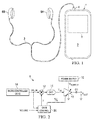
- FIG. 1 is an illustration of an example personal audio device 1 , in accordance with embodiments of the present disclosure.
- FIG. 1 depicts personal audio device 1 coupled to a headset 3 in the form of a pair of earbud speakers 8 A and 8 B.
- Headset 3 depicted in FIG. 1 is merely an example, and it is understood that personal audio device 1 may be used in connection with a variety of audio transducers, including without limitation, headphones, earbuds, in-ear earphones, and external speakers.
- a plug 4 may provide for connection of headset 3 to an electrical terminal of personal audio device 1 .
- Personal audio device 1 may provide a display to a user and receive user input using a touch screen 2 , or alternatively, a standard liquid crystal display (LCD) may be combined with various buttons, sliders, and/or dials disposed on the face and/or sides of personal audio device 1 . As also shown in FIG. 1 , personal audio device 1 may include an audio integrated circuit (IC) 9 for generating an analog audio signal for transmission to headset 3 and/or another audio transducer.
- IC audio integrated circuit
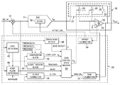
- FIG. 2 is a block diagram of selected components of an example audio IC 9 of a personal audio device, in accordance with embodiments of the present disclosure.
- a microcontroller core 18 may supply a digital audio input signal DIG_IN to a digital gain element 12 to apply a selectable digital gain x selected by gain control 20 to the digital input signal DIG_IN.
- the amplified digital audio input signal may be communicated to a digital-to-analog converter (DAC) 14 , which may convert the digital audio input signal to an analog signal Y IN .
- DAC digital-to-analog converter
- digital gain element 12 and DAC 14 may be referred to herein as a digital path portion of the signal path from the input node for digital audio input signal DIG_IN to the output node for output voltage signal V OUT depicted in FIG. 2 .
- digital gain element 12 and DAC 14 may sometimes be referred to as an audio compressor.
- DAC 14 may supply analog signal V IN to an amplifier stage 16 which may amplify or attenuate audio input signal V IN in conformity with a selectable analog gain k/x to provide an audio output signal V OUT , which may operate a speaker, headphone transducer, a line level signal output, and/or other suitable output.
- Amplifier stage 16 may be referred to herein as an analog path portion of the signal path from the input node for digital audio input signal DIG_IN to the output node for output voltage signal V OUT depicted in FIG. 2 .
- amplifier stage 16 may sometimes be referred to as an audio expander.
- a capacitor CO may be utilized to couple the output signal to the transducer or line level output, particularly if amplifier stage 16 is operated from a unipolar power supply having a quiescent voltage substantially differing from ground.
- a power supply 10 may provide the power supply rail inputs of amplifier stage 16 .
- audio IC 9 may include a gain control circuit 20 configured to, based on digital audio input signal DIG_IN, control selectable digital gain x of gain element 12 and a selectable analog gain k/x of amplifier stage 16 .
- a volume control signal may be provided from a microcontroller or other digital control circuit responsive to a user interface, volume knob encoder or program command, or other suitable mechanism.
- gain control circuit 20 may select a first digital gain (e.g., x 1 ) for the selectable digital gain and a first analog gain (e.g., k/x 1 ) for the selectable analog gain.
- gain control circuit 20 may select a second digital gain (e.g., x 2 ) greater than the first digital gain (e.g., x 2 >x 1 ) for the selectable digital gain and a second analog gain (e.g., k/x 2 ) lesser than the first analog gain (e.g., k/x 2 ⁇ k/x 1 ) for the selectable analog gain.
- a second digital gain e.g., x 2
- first digital gain e.g., x 2 >x 1
- second analog gain e.g., k/x 2
- the cumulative path gain (e.g., k) of the selectable digital gain and the selectable analog gain may be substantially constant (e.g., the same within manufacturing and/or operating tolerances of audio IC 9 ).
- k may be approximately equal to 1, such that the cumulative path gain is a unity gain.
- Such modification of digital gain and analog gain may increase the dynamic range of audio IC 9 compared to approaches in which the digital gain and analog gain are static, as it may reduce the noise injected into audio output signal V OUT , which noise may be a generally monotonically increasing function of the analog gain of amplifier stage 16 .
- the amount of noise injected into audio output signal V OUT may be reduced, while the signal level of audio output signal V OUT may be maintained in accordance with the digital audio input signal DIG_IN through application of a digital gain to gain element 12 inversely proportional to the analog gain.
- FIG. 3 is a block diagram of selected components of an example gain control circuit 20 for use within audio IC 9 , and selected components of audio IC 9 which may be coupled to gain control circuit 20 , in accordance with embodiments of the present disclosure.
- gain control circuit 20 may include a level detection circuit 42 , a comparator block 46 , a signal tracking block 47 , a zero-cross detection circuit 48 , a glitch correction circuit 44 , a gain calibration circuit 52 , an offset calibration circuit 54 , a noise floor detection circuit 56 , and a gain control state machine 50 .
- Level detection circuit 42 may include any suitable system, device, or apparatus for receiving digital audio input signal DIG_IN (or a derivative thereof), determining a magnitude of such signal, and outputting a signal indicative of such magnitude.
- Comparator block 46 may compare the output signal of level detection circuit 42 with N predetermined threshold magnitudes, wherein N is a positive integer, and based on such comparison, output a signal COMP_OUT (which may comprise N bits) indicative of whether the desired magnitude of audio output signal V OUT is greater or lesser than each of such predetermined threshold magnitudes.
- such predetermined threshold magnitudes may be relative to a full-scale voltage of digital audio input signal DIG_IN and/or audio output signal V OUT .
- comparator block 46 may implement hysteresis, such that signal COMP_OUT or a bit thereof may only transition if the output signal of level detection block 42 remains above or below a predetermined threshold magnitude for a minimum duration of time (e.g., 0.1 seconds to place any switching artifacts outside the human-perceptible audio range).
- Zero-cross detection circuit 48 may include any suitable system, device, or apparatus for detecting the occurrence of a zero crossing of a digital audio input signal (or a derivative thereof) and outputting a signal ZERO_DETECT indicating that a zero crossing of such signal has occurred.
- a zero crossing of a signal may occur when the waveform of such signal crosses a magnitude of zero or crosses another level within a threshold of zero and indicative of a zero crossing (e.g., a low signal level of lower than ⁇ 70 dB or within a small number of least significant bits of zero).
- Signal tracking block 47 may comprise any suitable system, device, or apparatus for tracking a particular parameter of an audio signal, including without limitation a plurality of peaks of such audio signal and/or a signal envelope of such audio signal, and based thereon, generate an output signal TRACKING indicative of such tracked parameter.
- Glitch correction circuit 44 may comprise any suitable system, device, or apparatus for correcting for a latency or group delay between the output of gain element 12 and the input of amplifier stage 16 .
- Such glitch correction may account for a change of the selectable digital gain of gain element 12 which requires a latency to propagate to amplifier stage 16 where a corresponding selectable analog gain may be applied. Without such correction, the latency of group delay may cause audio artifacts to appear at the output of the signal path.
- Gain calibration circuit 52 may comprise any suitable system, device, or apparatus for correcting for a non-ideal gain of amplifier stage 16 .
- amplifier stage 16 may comprise an operational amplifier 22 and a switched resistor network 24 comprising a resistor string 28 having a plurality of taps each coupled to a corresponding switch 29 .
- switches 29 may be selectively opened and closed to create an effective resistance between a negative input of operational amplifier 22 and the output of operational amplifier 22 , wherein the selectable analog gain of operational amplifier 22 is based on such effective resistance.
- gain calibration circuit 52 may determine the actual gain of amplifier stage 16 and output a signal GAIN_CAL indicative of such actual gain, and gain control state machine 50 may correct for non-idealities in selecting the selectable digital gain.
- Offset calibration circuit 54 may comprise any suitable system, device, or apparatus for correcting for an offset of amplifier stage 16 .
- operational amplifier 22 may include, due to non-idealities of amplifier stage 16 (e.g., temperature variations, process tolerances, etc.), a slight offset 26 from a desired ground or common mode voltage associated with amplifier stage 16 , which may affect signal output V OUT .
- offset calibration circuit 54 may determine the offset 26 of amplifier stage 16 and output a signal OFFSET_CAL, which may be communicated to an offset block 32 of DAC 14 such that DAC 14 may correct for such analog offset.
- Noise floor detection circuit 56 may comprise any suitable system, device, or apparatus for detecting a noise floor associated with digital audio input signal DIG_IN (or a derivative thereof), and generating a signal NOISE indicative of such detected noise floor.
- FIG. 4 is a block diagram of selected components of an example noise floor detection circuit 56 , in accordance with embodiments of the present disclosure.
- noise floor detection circuit 56 may include a fast Fourier transform block 60 configured to determine the noise floor of digital audio input signal DIG_IN (or a derivative thereof) by performing a fast Fourier transform of the audio signal.
- noise floor detection circuit 56 may receive a signal ANTI-NOISE indicative of an adaptive noise cancellation anti-noise signal present in digital audio input signal DIG_IN, and utilize an adaptive noise cancellation (ANC) analysis block 62 to determine the noise floor of digital audio input signal DIG_IN (or a derivative thereof) by determining a noise characteristic (e.g., signal-to-noise ratio, noise floor, etc.) of such anti-noise signal.
- ANC adaptive noise cancellation
- noise floor detection circuit 56 may include a bit width determination block 64 configured to determine the noise floor of digital audio input signal DIG_IN (or a derivative thereof) by determining a bit width (e.g., number of digital bits) of digital audio input signal DIG_IN (or a derivative thereof), as the noise floor of digital audio input signal DIG_IN is limited by its resolution.
- bit width determination block 64 configured to determine the noise floor of digital audio input signal DIG_IN (or a derivative thereof) by determining a bit width (e.g., number of digital bits) of digital audio input signal DIG_IN (or a derivative thereof), as the noise floor of digital audio input signal DIG_IN is limited by its resolution.
- noise floor detection circuit 56 may include a filter 66 and filtered signal analysis block 68 .
- gain control circuit 20 may, in connection with microcontroller core 18 , cause digital audio input signal DIG_IN (or a derivative thereof) to have known characteristics (e.g., generate a test signal with known spectral content).
- filter 66 may filter digital audio input signal DIG_IN (or a derivative thereof) to generate a filtered audio signal having frequencies with high spectral content filtered out
- filtered signal analysis block 68 may analyze the filtered audio signal, which may be expected to have a low magnitude across its entire frequency range, to determine the noise floor.
- noise floor detection circuit 56 may include a low-magnitude analysis block 70 configured to determine the noise floor of the audio signal by analyzing the audio signal during a period of time when digital audio input signal DIG_IN (or a derivative thereof) is expected to have a low or zero amplitude (e.g., as indicated by a signal generated by level detection circuit 42 ) and determining the noise floor based on such analysis.
- DIG_IN digital audio input signal
- level detection circuit 42 may include a low-magnitude analysis block 70 configured to determine the noise floor of the audio signal by analyzing the audio signal during a period of time when digital audio input signal DIG_IN (or a derivative thereof) is expected to have a low or zero amplitude (e.g., as indicated by a signal generated by level detection circuit 42 ) and determining the noise floor based on such analysis.
- noise floor detection circuit 56 may also include a fusion logic block 72 configured to, based on the noise floor levels output by each of fast Fourier transform block 60 , adaptive noise cancellation (ANC) analysis block 62 , bit width determination block 64 , filtered signal analysis block 68 , and low-magnitude analysis block 70 , determine an estimated noise floor of digital audio input signal DIG_IN (or a derivative thereof) and output a signal NOISE indicative of such determined estimated noise floor.
- ANC adaptive noise cancellation
- fusion logic block 72 may simply select the highest noise floor level of the noise floor levels output by each of fast Fourier transform block 60 , adaptive noise cancellation (ANC) analysis block 62 , bit width determination block 64 , filtered signal analysis block 68 , and low-magnitude analysis block 70 .
- ANC adaptive noise cancellation
- noise floor detection circuit 56 comprising fast Fourier transform block 60 , adaptive noise cancellation (ANC) analysis block 62 , bit width determination block 64 , filtered signal analysis block 68 , and low-magnitude analysis block 70
- noise floor detection circuit 56 may not include one or more of fast Fourier transform block 60 , adaptive noise cancellation (ANC) analysis block 62 , bit width determination block 64 , filtered signal analysis block 68 , and low-magnitude analysis block 70 .
- noise floor detection circuit 56 may include only one of fast Fourier transform block 60 , adaptive noise cancellation (ANC) analysis block 62 , bit width determination block 64 , filtered signal analysis block 68 , and low-magnitude analysis block 70 , in which case noise floor detection circuit 56 may not include fusion logic block 72 .
- ANC adaptive noise cancellation
- gain control state machine 50 may receive signals COMP_OUT, TRACKING, ZERO_DETECT, GLITCH, GAIN_CAL, and/or NOISE and based on one or more of such signals, generate the selectable digital gain and the selectable analog gain, as described in greater detail elsewhere in this disclosure. For example, when the magnitude of digital audio input signal DIG_IN transitions from above to below a predetermined threshold magnitude (e.g., ⁇ 24 dB), signal COMP_OUT may indicate such transition and in response, gain control state machine 50 may wait until the occurrence of a zero crossing (as indicated by signal ZERO_DETECT), after which it may cause DAC 14 to increase the selectable digital gain and decrease the selectable audio gain a similar amount.
- a predetermined threshold magnitude e.g., ⁇ 24 dB
- the change and any auditory artifacts associated with the change may be masked and therefore unnoticeable or less noticeable to a listener of an audio device including audio IC 9 .
- signal COMP_OUT may indicate such transition, and in response gain control state machine 50 may cause DAC 14 to decrease the selectable digital gain and increase the selectable audio gain in a similar amount.
- a predetermined threshold magnitude e.g., ⁇ 24 dB
- signal COMP_OUT may indicate such transition, and in response gain control state machine 50 may cause DAC 14 to decrease the selectable digital gain and increase the selectable audio gain in a similar amount.
- gain control circuit 20 may facilitate switching between gain modes to increase dynamic range while reducing audio artifacts.
- gain control circuit 20 may reduce audio artifacts associated with switching between a non-unity gain mode and a unity gain mode by implementing three or more intermediate dynamic range modes having step sizes between the various dynamic range modes. For instance, in some embodiments, gain control circuit 20 may implement eight intermediate dynamic range modes wherein the selectable digital gains have step sizes of 3 dB between the various modes such that the various modes have selectable digital gains of ⁇ 24 dB, ⁇ 21 dB, ⁇ 18 dB, ⁇ 15 dB, ⁇ 12 dB, ⁇ 9 dB, ⁇ 6 dB, ⁇ 3 dB and 0dB and respective selectable analog gains of 24 dB, 21 dB, 18 dB, 15 dB, 12 dB, 9 dB, 6 dB, 3 dB and 0 dB.
- gain control circuit 20 may cause the selectable digital gain to change from its minimum to maximum value, and cause the selectable digital gain to change from its maximum to minimum value in a series of steps, wherein each step may occur after a predetermined period of time.
- gain control circuit 20 may be configured to transition between the respective gain modes and a plurality of respective predetermined threshold magnitude levels.
- gain control circuit 20 may transition between the ⁇ 24 dB gain mode and the ⁇ 21 dB gain mode in response to the magnitude of the output signal crossing ⁇ 24 dB, may transition between the ⁇ 21 dB mode and the ⁇ 18 dB mode in response to the magnitude of the output signal crossing ⁇ 21 dB, may transition between the ⁇ 18 dB mode and the ⁇ 15 dB mode in response to the magnitude of the output signal crossing ⁇ 18 dB, and so on.
- gain control circuit 20 may also be configured to, using some or all of the methods previously described, predict a crossing of a particular threshold level, and based on such predicting, switch between the various modes at approximate occurrence of a zero crossing of the output signal, so as to reduce audio artifacts.
- gain control circuit 20 may be configured to predict when digital audio input signal DIG_IN crosses a primary threshold by receiving digital audio input signal DIG_IN and processing such signal before the signal propagates to gain element 12 and amplifier stage 16 , such that gain control circuit 20 may determine and apply the desired selectable digital gain and selectable audio gain at or before the signal propagates to such gain elements.
- gain control state machine 50 may also control modification of the selectable digital gain and the selectable analog gain based on the noise floor signal NOISE communicated from noise floor detection circuit 56 .
- dynamic range enhancement provided by modifying of the selectable digital gain and the selectable analog gain may be limited, as dynamic range enhancement may be unable to improve the noise floor already present in digital audio input signal DIG_IN.
- gain control state machine 50 may control the modification of the selectable digital gain and the selectable analog gain to limit the application of dynamic range enhancement in audio IC 9 .
- gain control state machine 50 may control modification of the selectable digital gain and the selectable analog gain based on the noise floor by limiting ranges of the selectable digital gain and the selectable analog gain based on the noise floor.
- the noise floor of digital audio input signal DIG_IN may be such that no improvement of signal quality may occur above a particular value of the selectable digital gain intermediate to the minimum and maximum selectable digital gain, and thus, gain control state machine 50 may limit the selectable digital gain to such particular value, and similarly limit the selectable analog gain.
- the noise floor of digital audio input signal DIG_IN may be such that no improvement of signal quality may occur above the minimum selectable digital gain, in which case gain control state machine 50 may limit the selectable digital gain to its minimum value, and the selectable analog gain to its maximum value.
- gain control state machine 50 may control modification of the selectable digital gain and the selectable analog gain based on the noise floor by controlling a switching time of modifying at least one of the selectable digital gain and the selectable analog gain based on the noise floor. Control of a switching time may allow for switching at an “optimal” time in order to reduce or eliminate audile artifacts caused by the switching while also preventing signal clipping.
- gain control state machine 50 may control modification of the selectable digital gain and the selectable analog gain based on the noise floor by controlling a step size of a change of at least one of the selectable digital gain and the selectable analog gain during the switching between gain modes based on the noise floor. Control of step size may reduce or eliminate audible artifacts associated with switching and minimize unnecessary switching between gain modes.
- gain control state machine 50 may control modification of the selectable digital gain and the selectable analog gain based on the noise floor by delaying modification of the selectable digital gain and the selectable analog gain based on the noise floor.
- other signals communicated to gain control state machine 50 e.g., change in magnitude of digital audio input signal DIG_IN, a zero-crossing of digital audio input signal DIG_IN, etc. may provide an indication to switch between gain modes.
- gain control state machine 50 may delay such switch until such time that the noise floor of digital audio input signal DIG_IN improves to a level in which such switch would affect signal quality.
- gain control state machine 50 may control modification of the selectable digital gain and the selectable analog gain based on the noise floor by ceasing switching between gain modes based on the noise floor. For instance, in some situations, other signals communicated to gain control state machine 50 (e.g., change in magnitude of digital audio input signal DIG_IN, a zero-crossing of digital audio input signal DIG_IN, etc.) may provide an indication to switch between gain modes. However, if the noise floor of digital audio input signal DIG_IN is such that no improvement in signal quality may occur from such switch between gain modes, gain control state machine 50 may cease any switching between gain modes.
- other signals communicated to gain control state machine 50 e.g., change in magnitude of digital audio input signal DIG_IN, a zero-crossing of digital audio input signal DIG_IN, etc.
- gain control state machine 50 may cease any switching between gain modes.
- references in the appended claims to an apparatus or system or a component of an apparatus or system being adapted to, arranged to, capable of, configured to, enabled to, operable to, or operative to perform a particular function encompasses that apparatus, system, or component, whether or not it or that particular function is activated, turned on, or unlocked, as long as that apparatus, system, or component is so adapted, arranged, capable, configured, enabled, operable, or operative.
Landscapes
- Engineering & Computer Science (AREA)
- Power Engineering (AREA)
- Multimedia (AREA)
- Microelectronics & Electronic Packaging (AREA)
- Physics & Mathematics (AREA)
- Acoustics & Sound (AREA)
- Signal Processing (AREA)
- Theoretical Computer Science (AREA)
- Circuit For Audible Band Transducer (AREA)
Abstract
Description
- The present disclosure relates in general to circuits for audio devices, including without limitation personal audio devices, such as wireless telephones and media players, and more specifically, to systems and methods for adapting an application of dynamic range enhancement to an audio signal path in an audio device based on a noise floor of a signal.
- Personal audio devices, including wireless telephones, such as mobile/cellular telephones, cordless telephones, mp3 players, and other consumer audio devices, are in widespread use. Such personal audio devices may include circuitry for driving a pair of headphones or one or more speakers. Such circuitry often includes a power amplifier for driving an audio output signal to headphones or speakers.
- One particular characteristic of a personal audio device, which may affect its marketability and desirability, is the dynamic range of its audio output signal. Stated simply, the dynamic range is the ratio between the largest and smallest values of the audio output signal. One way to increase dynamic range is to apply a high gain to the power amplifier. However, noise present in an audio output signal may be a generally monotonically increasing function of the gain of the power amplifier, such that any increased dynamic range as a result of a high-gain amplifier may be offset by signal noise which may effectively mask lower-intensity audio signals.
- U.S. patent application Ser. No. 14/083,972, filed Nov. 19, 2013, entitled “Enhancement of Dynamic Range of Audio Signal Path,” and assigned to the applicant (Cirrus Logic, Inc.) of the present disclosure (the “'972 Application”) discloses methods and systems for enhancing the dynamic range of an audio signal path. In the '972 Application, an apparatus for providing an output signal to an audio transducer includes an analog signal path portion, a digital-to-analog converter (DAC), and a control circuit. The analog signal path portion has an audio input for receiving an analog signal, an audio output for providing the output signal, and a selectable analog gain, and may be configured to generate the output signal based on the analog signal and in conformity with the selectable analog gain. The DAC has a selectable digital gain and may be configured to convert a digital audio input signal into the analog signal in conformity with the selectable digital gain. The control circuit may be configured to select the selectable analog gain and select the selectable digital gain based on a magnitude of a signal indicative of the output signal.
- In accordance with the teachings of the present disclosure, one or more disadvantages and problems associated with existing approaches to dynamic range enhancement of an audio signal path may be reduced or eliminated.
- In accordance with embodiments of the present disclosure, an apparatus for providing an output signal to an audio transducer may include a signal path and a control circuit. The signal path may include an analog signal path portion having an audio input for receiving an analog signal, an audio output for providing an output signal, and a selectable analog gain, and configured to generate the output signal based on the analog signal and in conformity with the selectable analog gain and a digital path portion having a selectable digital gain and configured to receive a digital input signal and convert the digital input signal into the analog signal in conformity with the selectable digital gain. The control circuit may be configured to modify the selectable digital gain and the selectable analog gain in response to an indication to switch between gain modes of the signal path, determine a noise floor of an audio signal comprising the digital input signal or a signal derived therefrom, and control modification of the selectable digital gain and the selectable analog gain based on the noise floor.
- In accordance with these and other embodiments of the present disclosure, a method may include a signal path comprising an analog signal path portion having an audio input for receiving an analog signal, an audio output for providing an output signal, and a selectable analog gain, and configured to generate the output signal based on the analog signal and in conformity with the selectable analog gain and further comprising a digital path portion having a selectable digital gain and configured to receive a digital input signal and convert the digital input signal into the analog signal in conformity with the selectable digital gain, modifying the selectable digital gain and the selectable analog gain in response to an indication to switch between gain modes of the signal path. The method may also include determining a noise floor of an audio signal comprising the digital input signal or a signal derived therefrom and controlling modification of the selectable digital gain and the selectable analog gain based on the noise floor.
- Technical advantages of the present disclosure may be readily apparent to one skilled in the art from the figures, description and claims included herein. The objects and advantages of the embodiments will be realized and achieved at least by the elements, features, and combinations particularly pointed out in the claims.
- It is to be understood that both the foregoing general description and the following detailed description are examples and explanatory and are not restrictive of the claims set forth in this disclosure.
- A more complete understanding of the present embodiments and advantages thereof may be acquired by referring to the following description taken in conjunction with the accompanying drawings, in which like reference numbers indicate like features, and wherein:
-
FIG. 1 is an illustration of an example personal audio device, in accordance with embodiments of the present disclosure; -
FIG. 2 is a block diagram of selected components of an example audio integrated circuit of a personal audio device, in accordance with embodiments of the present disclosure; -
FIG. 3 is a block diagram of selected components of an example gain control circuit for use within the audio integrated circuit depicted inFIG. 2 , and selected components of an audio integrated circuit which may be coupled to the gain control circuit, in accordance with embodiments of the present disclosure; and -
FIG. 4 is a block diagram of selected components of an example noise floor detection circuit for use within the gain control circuit depicted inFIG. 3 , in accordance with embodiments of the present disclosure. - In accordance with embodiments of the present disclosure, an integrated circuit for use in an audio device, such as a personal audio device (e.g., mobile telephone, portable music player, tablet computer, personal digital assistant, etc.), may include a signal path having a digital path portion (e.g., an audio compressor) and an analog path portion (e.g., an audio expander). The digital path portion may be configured to receive a digital input signal (e.g., a digital audio signal), apply a selectable digital gain x to the digital input signal, and convert the digital input signal (e.g., via a digital-to-analog converter) to an analog signal in conformity with the selectable digital gain. The analog path portion may be configured to receive the analog signal and apply (e.g., by an analog amplifier) a selectable analog gain k/x to the analog signal to generate an output signal, wherein said output signal may be communicated to a loudspeaker for playback and/or to other circuitry for processing. The numerator k of the selectable analog gain may be a constant defining an overall cumulative gain of the signal path. A control circuit coupled to the signal path may be capable of modifying the selectable digital gain and the selectable analog gain, for example to maximize a dynamic range of the signal path. For example, based on analysis of the output signal or another signal within the signal path indicative of the output signal, the control circuit may select a value for the selectable digital gain and a corresponding value for the selectable analog gain. Thus, for lower magnitudes of the output signal, the control circuit may select a higher selectable digital gain and a lower selectable analog gain, and for higher magnitudes of the output signal, the control circuit may select a lower selectable digital gain and a higher selectable analog gain. Such selectable gains may allow a signal path to increase its dynamic range to lower-magnitude signals, while preventing undesirable effects such as signal clipping for higher-magnitude signals. In operation, the control circuit may also be configured to predict, based on a magnitude of a signal indicative of the output signal, a condition for changing the selectable digital gain and the selectable analog gain, and responsive to predicting the occurrence of the condition, change, at an approximate time in which a zero crossing of the signal indicative of the output signal occurs, the selectable digital gain and the selectable analog gain.
- The integrated circuit described above may be used in any suitable system, device, or apparatus, including without limitation, a personal audio device.
FIG. 1 is an illustration of an example personal audio device 1, in accordance with embodiments of the present disclosure.FIG. 1 depicts personal audio device 1 coupled to a headset 3 in the form of a pair ofearbud speakers FIG. 1 is merely an example, and it is understood that personal audio device 1 may be used in connection with a variety of audio transducers, including without limitation, headphones, earbuds, in-ear earphones, and external speakers. A plug 4 may provide for connection of headset 3 to an electrical terminal of personal audio device 1. Personal audio device 1 may provide a display to a user and receive user input using atouch screen 2, or alternatively, a standard liquid crystal display (LCD) may be combined with various buttons, sliders, and/or dials disposed on the face and/or sides of personal audio device 1. As also shown inFIG. 1 , personal audio device 1 may include an audio integrated circuit (IC) 9 for generating an analog audio signal for transmission to headset 3 and/or another audio transducer. -
FIG. 2 is a block diagram of selected components of an example audio IC 9 of a personal audio device, in accordance with embodiments of the present disclosure. As shown inFIG. 2 , amicrocontroller core 18 may supply a digital audio input signal DIG_IN to adigital gain element 12 to apply a selectable digital gain x selected bygain control 20 to the digital input signal DIG_IN. The amplified digital audio input signal may be communicated to a digital-to-analog converter (DAC) 14, which may convert the digital audio input signal to an analog signal YIN. Together,digital gain element 12 andDAC 14 may be referred to herein as a digital path portion of the signal path from the input node for digital audio input signal DIG_IN to the output node for output voltage signal VOUT depicted inFIG. 2 . In the relevant art,digital gain element 12 andDAC 14 may sometimes be referred to as an audio compressor. -
DAC 14 may supply analog signal VIN to anamplifier stage 16 which may amplify or attenuate audio input signal VIN in conformity with a selectable analog gain k/x to provide an audio output signal VOUT, which may operate a speaker, headphone transducer, a line level signal output, and/or other suitable output.Amplifier stage 16 may be referred to herein as an analog path portion of the signal path from the input node for digital audio input signal DIG_IN to the output node for output voltage signal VOUT depicted inFIG. 2 . In the relevant art,amplifier stage 16 may sometimes be referred to as an audio expander. A capacitor CO may be utilized to couple the output signal to the transducer or line level output, particularly ifamplifier stage 16 is operated from a unipolar power supply having a quiescent voltage substantially differing from ground. Apower supply 10 may provide the power supply rail inputs ofamplifier stage 16. - As shown in
FIG. 2 , audio IC 9 may include again control circuit 20 configured to, based on digital audio input signal DIG_IN, control selectable digital gain x ofgain element 12 and a selectable analog gain k/x ofamplifier stage 16. In embodiments in which a volume control is present, a volume control signal may be provided from a microcontroller or other digital control circuit responsive to a user interface, volume knob encoder or program command, or other suitable mechanism. - As an example of the dynamic range enhancement functionality of audio IC 9, when digital audio input signal DIG_IN is at or near zero decibels (0 dB) relative to the full-scale voltage of the digital audio input signal,
gain control circuit 20 may select a first digital gain (e.g., x1) for the selectable digital gain and a first analog gain (e.g., k/x1) for the selectable analog gain. However, if the magnitude of digital audio input signal DIG_IN is below a particular predetermined threshold magnitude relative to the full-scale voltage of digital audio input signal DIG_IN (e.g., −20 dB),gain control circuit 20 may select a second digital gain (e.g., x2) greater than the first digital gain (e.g., x2>x1) for the selectable digital gain and a second analog gain (e.g., k/x2) lesser than the first analog gain (e.g., k/x2<k/x1) for the selectable analog gain. In each case, the cumulative path gain (e.g., k) of the selectable digital gain and the selectable analog gain may be substantially constant (e.g., the same within manufacturing and/or operating tolerances of audio IC 9). In some embodiments, k may be approximately equal to 1, such that the cumulative path gain is a unity gain. Such modification of digital gain and analog gain may increase the dynamic range of audio IC 9 compared to approaches in which the digital gain and analog gain are static, as it may reduce the noise injected into audio output signal VOUT, which noise may be a generally monotonically increasing function of the analog gain ofamplifier stage 16. While such noise may be negligible for higher magnitude audio signals (e.g., at or near 0 dB relative to full-scale voltage), the presence of such noise may become noticeable for lower magnitude audio signals (e.g., at or near −20 dB or lower relative to full-scale voltage). By applying a smaller analog gain atamplifier stage 16 for smaller signal magnitudes, the amount of noise injected into audio output signal VOUT may be reduced, while the signal level of audio output signal VOUT may be maintained in accordance with the digital audio input signal DIG_IN through application of a digital gain to gainelement 12 inversely proportional to the analog gain. -
FIG. 3 is a block diagram of selected components of an examplegain control circuit 20 for use within audio IC 9, and selected components of audio IC 9 which may be coupled to gaincontrol circuit 20, in accordance with embodiments of the present disclosure. As shown inFIG. 3 , gaincontrol circuit 20 may include alevel detection circuit 42, acomparator block 46, asignal tracking block 47, a zero-cross detection circuit 48, aglitch correction circuit 44, again calibration circuit 52, an offsetcalibration circuit 54, a noisefloor detection circuit 56, and a gaincontrol state machine 50.Level detection circuit 42 may include any suitable system, device, or apparatus for receiving digital audio input signal DIG_IN (or a derivative thereof), determining a magnitude of such signal, and outputting a signal indicative of such magnitude.Comparator block 46 may compare the output signal oflevel detection circuit 42 with N predetermined threshold magnitudes, wherein N is a positive integer, and based on such comparison, output a signal COMP_OUT (which may comprise N bits) indicative of whether the desired magnitude of audio output signal VOUT is greater or lesser than each of such predetermined threshold magnitudes. In some embodiments, such predetermined threshold magnitudes may be relative to a full-scale voltage of digital audio input signal DIG_IN and/or audio output signal VOUT. In some embodiments,comparator block 46 may implement hysteresis, such that signal COMP_OUT or a bit thereof may only transition if the output signal oflevel detection block 42 remains above or below a predetermined threshold magnitude for a minimum duration of time (e.g., 0.1 seconds to place any switching artifacts outside the human-perceptible audio range). - Zero-
cross detection circuit 48 may include any suitable system, device, or apparatus for detecting the occurrence of a zero crossing of a digital audio input signal (or a derivative thereof) and outputting a signal ZERO_DETECT indicating that a zero crossing of such signal has occurred. A zero crossing of a signal may occur when the waveform of such signal crosses a magnitude of zero or crosses another level within a threshold of zero and indicative of a zero crossing (e.g., a low signal level of lower than −70 dB or within a small number of least significant bits of zero). - Signal tracking
block 47 may comprise any suitable system, device, or apparatus for tracking a particular parameter of an audio signal, including without limitation a plurality of peaks of such audio signal and/or a signal envelope of such audio signal, and based thereon, generate an output signal TRACKING indicative of such tracked parameter. -
Glitch correction circuit 44 may comprise any suitable system, device, or apparatus for correcting for a latency or group delay between the output ofgain element 12 and the input ofamplifier stage 16. Such glitch correction may account for a change of the selectable digital gain ofgain element 12 which requires a latency to propagate toamplifier stage 16 where a corresponding selectable analog gain may be applied. Without such correction, the latency of group delay may cause audio artifacts to appear at the output of the signal path. -
Gain calibration circuit 52 may comprise any suitable system, device, or apparatus for correcting for a non-ideal gain ofamplifier stage 16. To illustrate,amplifier stage 16 may comprise anoperational amplifier 22 and a switchedresistor network 24 comprising aresistor string 28 having a plurality of taps each coupled to acorresponding switch 29. To apply a desired selectable analog gain toamplifier stage 16, switches 29 may be selectively opened and closed to create an effective resistance between a negative input ofoperational amplifier 22 and the output ofoperational amplifier 22, wherein the selectable analog gain ofoperational amplifier 22 is based on such effective resistance. However, due to non-idealities of amplifier stage 16 (e.g., temperature variations, process tolerances, etc.), an actual gain ofamplifier stage 16 may differ from that of a desired level of gain determined by gaincontrol state machine 50. Accordingly, gaincalibration circuit 52 may determine the actual gain ofamplifier stage 16 and output a signal GAIN_CAL indicative of such actual gain, and gaincontrol state machine 50 may correct for non-idealities in selecting the selectable digital gain. - Offset
calibration circuit 54 may comprise any suitable system, device, or apparatus for correcting for an offset ofamplifier stage 16. To illustrate,operational amplifier 22 may include, due to non-idealities of amplifier stage 16 (e.g., temperature variations, process tolerances, etc.), a slight offset 26 from a desired ground or common mode voltage associated withamplifier stage 16, which may affect signal output VOUT. Accordingly, offsetcalibration circuit 54 may determine the offset 26 ofamplifier stage 16 and output a signal OFFSET_CAL, which may be communicated to an offsetblock 32 ofDAC 14 such thatDAC 14 may correct for such analog offset. - Noise
floor detection circuit 56 may comprise any suitable system, device, or apparatus for detecting a noise floor associated with digital audio input signal DIG_IN (or a derivative thereof), and generating a signal NOISE indicative of such detected noise floor.FIG. 4 is a block diagram of selected components of an example noisefloor detection circuit 56, in accordance with embodiments of the present disclosure. As shown inFIG. 4 , in some embodiments, noisefloor detection circuit 56 may include a fastFourier transform block 60 configured to determine the noise floor of digital audio input signal DIG_IN (or a derivative thereof) by performing a fast Fourier transform of the audio signal. In these and other embodiments, as shown inFIGS. 3 and 4 , noisefloor detection circuit 56 may receive a signal ANTI-NOISE indicative of an adaptive noise cancellation anti-noise signal present in digital audio input signal DIG_IN, and utilize an adaptive noise cancellation (ANC)analysis block 62 to determine the noise floor of digital audio input signal DIG_IN (or a derivative thereof) by determining a noise characteristic (e.g., signal-to-noise ratio, noise floor, etc.) of such anti-noise signal. In these and other embodiments, as shown inFIG. 4 , noisefloor detection circuit 56 may include a bitwidth determination block 64 configured to determine the noise floor of digital audio input signal DIG_IN (or a derivative thereof) by determining a bit width (e.g., number of digital bits) of digital audio input signal DIG_IN (or a derivative thereof), as the noise floor of digital audio input signal DIG_IN is limited by its resolution. - In these and other embodiments, as shown in
FIG. 4 , noisefloor detection circuit 56 may include afilter 66 and filteredsignal analysis block 68. In such embodiments, gaincontrol circuit 20 may, in connection withmicrocontroller core 18, cause digital audio input signal DIG_IN (or a derivative thereof) to have known characteristics (e.g., generate a test signal with known spectral content). In operation, filter 66 may filter digital audio input signal DIG_IN (or a derivative thereof) to generate a filtered audio signal having frequencies with high spectral content filtered out, and filteredsignal analysis block 68 may analyze the filtered audio signal, which may be expected to have a low magnitude across its entire frequency range, to determine the noise floor. - In these and other embodiments, noise
floor detection circuit 56 may include a low-magnitude analysis block 70 configured to determine the noise floor of the audio signal by analyzing the audio signal during a period of time when digital audio input signal DIG_IN (or a derivative thereof) is expected to have a low or zero amplitude (e.g., as indicated by a signal generated by level detection circuit 42) and determining the noise floor based on such analysis. - As shown in
FIG. 4 , noisefloor detection circuit 56 may also include afusion logic block 72 configured to, based on the noise floor levels output by each of fastFourier transform block 60, adaptive noise cancellation (ANC)analysis block 62, bitwidth determination block 64, filteredsignal analysis block 68, and low-magnitude analysis block 70, determine an estimated noise floor of digital audio input signal DIG_IN (or a derivative thereof) and output a signal NOISE indicative of such determined estimated noise floor. In some embodiments,fusion logic block 72 may simply select the highest noise floor level of the noise floor levels output by each of fastFourier transform block 60, adaptive noise cancellation (ANC)analysis block 62, bitwidth determination block 64, filteredsignal analysis block 68, and low-magnitude analysis block 70. - Although
FIG. 4 depicts noisefloor detection circuit 56 comprising fastFourier transform block 60, adaptive noise cancellation (ANC)analysis block 62, bitwidth determination block 64, filteredsignal analysis block 68, and low-magnitude analysis block 70, in some embodiments, noisefloor detection circuit 56 may not include one or more of fastFourier transform block 60, adaptive noise cancellation (ANC)analysis block 62, bitwidth determination block 64, filteredsignal analysis block 68, and low-magnitude analysis block 70. In some of such embodiments, noisefloor detection circuit 56 may include only one of fastFourier transform block 60, adaptive noise cancellation (ANC)analysis block 62, bitwidth determination block 64, filteredsignal analysis block 68, and low-magnitude analysis block 70, in which case noisefloor detection circuit 56 may not includefusion logic block 72. - Turning again to
FIG. 3 , gaincontrol state machine 50 may receive signals COMP_OUT, TRACKING, ZERO_DETECT, GLITCH, GAIN_CAL, and/or NOISE and based on one or more of such signals, generate the selectable digital gain and the selectable analog gain, as described in greater detail elsewhere in this disclosure. For example, when the magnitude of digital audio input signal DIG_IN transitions from above to below a predetermined threshold magnitude (e.g., −24 dB), signal COMP_OUT may indicate such transition and in response, gaincontrol state machine 50 may wait until the occurrence of a zero crossing (as indicated by signal ZERO_DETECT), after which it may causeDAC 14 to increase the selectable digital gain and decrease the selectable audio gain a similar amount. By changing the selectable digital gain and the selectable audio gain at a zero crossing of digital audio input signal DIN_IN (or a derivative thereof), the change and any auditory artifacts associated with the change may be masked and therefore unnoticeable or less noticeable to a listener of an audio device including audio IC 9. - As another example, when the sum of the magnitude of digital audio input signal DIG_IN transitions from below to above a predetermined threshold magnitude (e.g., −24 dB), signal COMP_OUT may indicate such transition, and in response gain
control state machine 50 may causeDAC 14 to decrease the selectable digital gain and increase the selectable audio gain in a similar amount. However, when transitioning to lower digital gain mode, it may not be desirable to wait for a zero cross of the output signal, as a transition from below to above the predetermined threshold magnitude may almost immediately lead to clipping of the audio signal. Accordingly, it may be desirable to predict whether the magnitude of digital audio input signal DIG_IN is likely to cross such predetermined threshold and modify the selectable digital gain and the selectable analog gain responsive to such prediction at a zero crossing event of the digital audio input signal DIG_IN occurring before crossing of the predetermined threshold by the digital audio input signal DIG_IN. By applying such predictive techniques, examples of which are explained in U.S. patent application Ser. No. 15/244,670 entitled “Enhancing Dynamic Range Based on Spectral Content of Signal,” and filed on Aug. 23, 2016, gaincontrol circuit 20 may facilitate switching between gain modes to increase dynamic range while reducing audio artifacts. - In these and other embodiments, gain
control circuit 20 may reduce audio artifacts associated with switching between a non-unity gain mode and a unity gain mode by implementing three or more intermediate dynamic range modes having step sizes between the various dynamic range modes. For instance, in some embodiments, gaincontrol circuit 20 may implement eight intermediate dynamic range modes wherein the selectable digital gains have step sizes of 3 dB between the various modes such that the various modes have selectable digital gains of −24 dB, −21 dB, −18 dB, −15 dB, −12 dB, −9 dB, −6 dB, −3 dB and 0dB and respective selectable analog gains of 24 dB, 21 dB, 18 dB, 15 dB, 12 dB, 9 dB, 6 dB, 3 dB and 0 dB. Thus, in response to the magnitude of the output signal crossing a relevant threshold, gaincontrol circuit 20 may cause the selectable digital gain to change from its minimum to maximum value, and cause the selectable digital gain to change from its maximum to minimum value in a series of steps, wherein each step may occur after a predetermined period of time. In addition, in some embodiments, gaincontrol circuit 20 may be configured to transition between the respective gain modes and a plurality of respective predetermined threshold magnitude levels. For example, gaincontrol circuit 20 may transition between the −24 dB gain mode and the −21 dB gain mode in response to the magnitude of the output signal crossing −24 dB, may transition between the −21 dB mode and the −18 dB mode in response to the magnitude of the output signal crossing −21 dB, may transition between the −18 dB mode and the −15 dB mode in response to the magnitude of the output signal crossing −18 dB, and so on. In these embodiments, gaincontrol circuit 20 may also be configured to, using some or all of the methods previously described, predict a crossing of a particular threshold level, and based on such predicting, switch between the various modes at approximate occurrence of a zero crossing of the output signal, so as to reduce audio artifacts. - In addition or alternatively to the embodiments discussed above, gain
control circuit 20 may be configured to predict when digital audio input signal DIG_IN crosses a primary threshold by receiving digital audio input signal DIG_IN and processing such signal before the signal propagates to gainelement 12 andamplifier stage 16, such thatgain control circuit 20 may determine and apply the desired selectable digital gain and selectable audio gain at or before the signal propagates to such gain elements. - In addition or alternatively to the functionality described above, gain
control state machine 50 may also control modification of the selectable digital gain and the selectable analog gain based on the noise floor signal NOISE communicated from noisefloor detection circuit 56. To illustrate, in situations when a noise floor of digital audio input signal DIG_IN is relatively high, dynamic range enhancement provided by modifying of the selectable digital gain and the selectable analog gain may be limited, as dynamic range enhancement may be unable to improve the noise floor already present in digital audio input signal DIG_IN. Accordingly, in such scenarios in which application of dynamic range enhancement by modifying of the selectable digital gain and the selectable analog gain has limited or no effect in increasing signal quality, gaincontrol state machine 50 may control the modification of the selectable digital gain and the selectable analog gain to limit the application of dynamic range enhancement in audio IC 9. - For example, in some embodiments, gain
control state machine 50 may control modification of the selectable digital gain and the selectable analog gain based on the noise floor by limiting ranges of the selectable digital gain and the selectable analog gain based on the noise floor. To illustrate, the noise floor of digital audio input signal DIG_IN may be such that no improvement of signal quality may occur above a particular value of the selectable digital gain intermediate to the minimum and maximum selectable digital gain, and thus, gaincontrol state machine 50 may limit the selectable digital gain to such particular value, and similarly limit the selectable analog gain. In some instances, the noise floor of digital audio input signal DIG_IN may be such that no improvement of signal quality may occur above the minimum selectable digital gain, in which case gaincontrol state machine 50 may limit the selectable digital gain to its minimum value, and the selectable analog gain to its maximum value. - As another example, in these and other embodiments, gain
control state machine 50 may control modification of the selectable digital gain and the selectable analog gain based on the noise floor by controlling a switching time of modifying at least one of the selectable digital gain and the selectable analog gain based on the noise floor. Control of a switching time may allow for switching at an “optimal” time in order to reduce or eliminate audile artifacts caused by the switching while also preventing signal clipping. - As another example, in these and other embodiments, gain
control state machine 50 may control modification of the selectable digital gain and the selectable analog gain based on the noise floor by controlling a step size of a change of at least one of the selectable digital gain and the selectable analog gain during the switching between gain modes based on the noise floor. Control of step size may reduce or eliminate audible artifacts associated with switching and minimize unnecessary switching between gain modes. - As an additional example, in these and other embodiments, gain
control state machine 50 may control modification of the selectable digital gain and the selectable analog gain based on the noise floor by delaying modification of the selectable digital gain and the selectable analog gain based on the noise floor. For instance, in some situations, other signals communicated to gain control state machine 50 (e.g., change in magnitude of digital audio input signal DIG_IN, a zero-crossing of digital audio input signal DIG_IN, etc.) may provide an indication to switch between gain modes. However, if the noise floor of digital audio input signal DIG_IN is such that no improvement in signal quality may occur from such switch between gain modes, gaincontrol state machine 50 may delay such switch until such time that the noise floor of digital audio input signal DIG_IN improves to a level in which such switch would affect signal quality. - As an additional example, in these and other embodiments, gain
control state machine 50 may control modification of the selectable digital gain and the selectable analog gain based on the noise floor by ceasing switching between gain modes based on the noise floor. For instance, in some situations, other signals communicated to gain control state machine 50 (e.g., change in magnitude of digital audio input signal DIG_IN, a zero-crossing of digital audio input signal DIG_IN, etc.) may provide an indication to switch between gain modes. However, if the noise floor of digital audio input signal DIG_IN is such that no improvement in signal quality may occur from such switch between gain modes, gaincontrol state machine 50 may cease any switching between gain modes. - This disclosure encompasses all changes, substitutions, variations, alterations, and modifications to the exemplary embodiments herein that a person having ordinary skill in the art would comprehend. Similarly, where appropriate, the appended claims encompass all changes, substitutions, variations, alterations, and modifications to the exemplary embodiments herein that a person having ordinary skill in the art would comprehend. Moreover, reference in the appended claims to an apparatus or system or a component of an apparatus or system being adapted to, arranged to, capable of, configured to, enabled to, operable to, or operative to perform a particular function encompasses that apparatus, system, or component, whether or not it or that particular function is activated, turned on, or unlocked, as long as that apparatus, system, or component is so adapted, arranged, capable, configured, enabled, operable, or operative.
- All examples and conditional language recited herein are intended for pedagogical objects to aid the reader in understanding the invention and the concepts contributed by the inventor to furthering the art, and are construed as being without limitation to such specifically recited examples and conditions. Although embodiments of the present inventions have been described in detail, it should be understood that various changes, substitutions, and alterations could be made hereto without departing from the spirit and scope of the disclosure.
Claims (22)
Priority Applications (2)
| Application Number | Priority Date | Filing Date | Title |
|---|---|---|---|
| US15/286,289 US9967665B2 (en) | 2016-10-05 | 2016-10-05 | Adaptation of dynamic range enhancement based on noise floor of signal |
| GB201700371A GB2558005B (en) | 2016-10-05 | 2017-01-10 | Adaptation of dynamic range enhancement based on noise floor of signal |
Applications Claiming Priority (1)
| Application Number | Priority Date | Filing Date | Title |
|---|---|---|---|
| US15/286,289 US9967665B2 (en) | 2016-10-05 | 2016-10-05 | Adaptation of dynamic range enhancement based on noise floor of signal |
Publications (2)
| Publication Number | Publication Date |
|---|---|
| US20180098149A1 true US20180098149A1 (en) | 2018-04-05 |
| US9967665B2 US9967665B2 (en) | 2018-05-08 |
Family
ID=58463742
Family Applications (1)
| Application Number | Title | Priority Date | Filing Date |
|---|---|---|---|
| US15/286,289 Active US9967665B2 (en) | 2016-10-05 | 2016-10-05 | Adaptation of dynamic range enhancement based on noise floor of signal |
Country Status (2)
| Country | Link |
|---|---|
| US (1) | US9967665B2 (en) |
| GB (1) | GB2558005B (en) |
Cited By (8)
| Publication number | Priority date | Publication date | Assignee | Title |
|---|---|---|---|---|
| US10263630B2 (en) | 2016-08-11 | 2019-04-16 | Cirrus Logic, Inc. | Multi-path analog front end with adaptive path |
| US10284217B1 (en) | 2014-03-05 | 2019-05-07 | Cirrus Logic, Inc. | Multi-path analog front end and analog-to-digital converter for a signal processing system |
| US10321230B2 (en) | 2017-04-07 | 2019-06-11 | Cirrus Logic, Inc. | Switching in an audio system with multiple playback paths |
| US20190214029A1 (en) * | 2018-01-10 | 2019-07-11 | Savitech Corp. | Audio processing method and non-transitory computer readable medium |
| US10447217B2 (en) | 2016-09-27 | 2019-10-15 | Cirrus Logic, Inc. | Amplifier with configurable final output stage |
| US10545561B2 (en) | 2016-08-10 | 2020-01-28 | Cirrus Logic, Inc. | Multi-path digitation based on input signal fidelity and output requirements |
| WO2021138060A1 (en) * | 2020-01-02 | 2021-07-08 | Cirrus Logic International Semiconductor Ltd. | Minimizing idle channel noise in a class-d pulse width modulation amplifier |
| US11699423B1 (en) * | 2022-01-25 | 2023-07-11 | Elite Semiconductor Microelectronics Technology Inc. | Apparatus for noise reduction in audio signal processing |
Families Citing this family (1)
| Publication number | Priority date | Publication date | Assignee | Title |
|---|---|---|---|---|
| US12375095B2 (en) * | 2023-03-14 | 2025-07-29 | Texas Instruments Incorporated | Digital-to-analog converter circuit with linear programmable gain stage |
Citations (8)
| Publication number | Priority date | Publication date | Assignee | Title |
|---|---|---|---|---|
| US20040078200A1 (en) * | 2002-10-17 | 2004-04-22 | Clarity, Llc | Noise reduction in subbanded speech signals |
| US20080114239A1 (en) * | 2006-11-10 | 2008-05-15 | Penrith Corporation | Transducer array imaging system |
| US20080292107A1 (en) * | 2007-01-23 | 2008-11-27 | Syfx Tekworks | Noise analysis and extraction systems and methods |
| US20110188671A1 (en) * | 2009-10-15 | 2011-08-04 | Georgia Tech Research Corporation | Adaptive gain control based on signal-to-noise ratio for noise suppression |
| US20120133411A1 (en) * | 2010-11-30 | 2012-05-31 | Qualcomm Incorporated | Adaptive gain adjustment system |
| US20130095870A1 (en) * | 2010-06-09 | 2013-04-18 | Andrew Llc | Uplink noise minimization |
| US20150170663A1 (en) * | 2012-08-27 | 2015-06-18 | Fraunhofer-Gesellschaft Zur Foerderung Der Angewandten Forschung E.V. | Apparatus and method for reproducing an audio signal, apparatus and method for generating a coded audio signal, computer program and coded audio signal |
| US9118401B1 (en) * | 2014-10-28 | 2015-08-25 | Harris Corporation | Method of adaptive interference mitigation in wide band spectrum |
Family Cites Families (181)
| Publication number | Priority date | Publication date | Assignee | Title |
|---|---|---|---|---|
| GB1599401A (en) | 1978-04-18 | 1981-09-30 | Nat Res Dev | Input signal level control for communications channels |
| JPS6052607B2 (en) | 1979-05-10 | 1985-11-20 | ヤマハ株式会社 | amplifier |
| US4441081A (en) | 1981-12-22 | 1984-04-03 | International Business Machines | Switching power driving circuit arrangement |
| US4446440A (en) | 1982-01-26 | 1984-05-01 | Hewlett-Packard Company | Dual mode amplifier |
| JPS58142614A (en) | 1982-02-18 | 1983-08-24 | Sony Corp | Gain controlling device |
| US4493091A (en) | 1982-05-05 | 1985-01-08 | Dolby Laboratories Licensing Corporation | Analog and digital signal apparatus |
| GB8705923D0 (en) | 1987-03-12 | 1987-04-15 | Gen Electric Co Plc | Analogue to digital converter |
| US5006851A (en) | 1988-07-18 | 1991-04-09 | Matsushita Electric Industrial Co., Ltd. | Analog-to-digital converting system |
| US4972436A (en) | 1988-10-14 | 1990-11-20 | Hayes Microcomputer Products, Inc. | High performance sigma delta based analog modem front end |
| US5111506A (en) | 1989-03-02 | 1992-05-05 | Ensonig Corporation | Power efficient hearing aid |
| JPH065819B2 (en) | 1989-06-29 | 1994-01-19 | ヤマハ株式会社 | A / D converter |
| US4999830A (en) | 1989-09-25 | 1991-03-12 | At&T Bell Laboratories | Communication system analog-to-digital converter using echo information to improve resolution |
| US5148167A (en) | 1990-04-06 | 1992-09-15 | General Electric Company | Sigma-delta oversampled analog-to-digital converter network with chopper stabilization |
| US5323159A (en) | 1990-04-20 | 1994-06-21 | Nakamichi Corporation | Digital/analog converter |
| US5198814A (en) | 1990-11-28 | 1993-03-30 | Nec Corporation | Digital-to-analog converter with conversion error compensation |
| US5077539A (en) | 1990-12-26 | 1991-12-31 | Apogee Technology, Inc. | Switching amplifier |
| US5272449A (en) | 1991-01-09 | 1993-12-21 | Kikusui Electronics Corporation | Vertical amplifier system for multitrace oscilloscope and method for calibrating the same |
| JPH05315856A (en) | 1992-05-14 | 1993-11-26 | Pioneer Electron Corp | Power amplifier |
| US5810477A (en) | 1993-04-30 | 1998-09-22 | International Business Machines Corporation | System for identifying surface conditions of a moving medium |
| DE19502047C2 (en) | 1995-01-12 | 1996-12-05 | Stage Tec Gmbh | Process for analog-digital conversion of signals |
| DK0707383T3 (en) | 1994-06-14 | 2002-08-19 | Stage Tec Entwicklungsgesellsc | Switching device for analog-digital switching of signals |
| US5550923A (en) | 1994-09-02 | 1996-08-27 | Minnesota Mining And Manufacturing Company | Directional ear device with adaptive bandwidth and gain control |
| JP2910825B2 (en) | 1994-10-20 | 1999-06-23 | 日本電気株式会社 | Digital image receiver |
| JPH09130245A (en) | 1995-11-06 | 1997-05-16 | Sony Corp | Variable gain circuit |
| US5796303A (en) | 1996-06-26 | 1998-08-18 | Vinn; Charles L. | Popless amplifier |
| JPH10257583A (en) | 1997-03-06 | 1998-09-25 | Asahi Chem Ind Co Ltd | Voice processing unit and its voice processing method |
| US6088461A (en) | 1997-09-26 | 2000-07-11 | Crystal Semiconductor Corporation | Dynamic volume control system |
| US6542612B1 (en) | 1997-10-03 | 2003-04-01 | Alan W. Needham | Companding amplifier with sidechannel gain control |
| JP3449254B2 (en) | 1997-11-14 | 2003-09-22 | ヤマハ株式会社 | D / A converter |
| US6333707B1 (en) | 1998-02-19 | 2001-12-25 | Nortel Networks Limited | Dynamic range extension of wideband receiver |
| US6160455A (en) | 1998-03-10 | 2000-12-12 | Indigo Manufacturing Inc. | Derived power supply for composite bridge amplifiers |
| JPH11340831A (en) | 1998-05-29 | 1999-12-10 | Toa Corp | High precision a/d converter |
| JP2000029736A (en) | 1998-07-13 | 2000-01-28 | Oki Electric Ind Co Ltd | Semiconductor integrated circuit |
| US6271780B1 (en) | 1998-10-08 | 2001-08-07 | Cirrus Logic, Inc. | Gain ranging analog-to-digital converter with error correction |
| US6229390B1 (en) | 1999-03-09 | 2001-05-08 | Tripath Technology, Inc. | Methods and apparatus for noise shaping a mixed signal power output |
| DE10021824C2 (en) | 1999-05-07 | 2002-01-31 | Yamaha Corp | D / A converter device and D / A converter method |
| US7020892B2 (en) | 1999-09-03 | 2006-03-28 | Lsi Logic Corporation | Time-shifted video signal processing |
| EP1119145A1 (en) | 2000-01-20 | 2001-07-25 | TELEFONAKTIEBOLAGET LM ERICSSON (publ) | Parallel decision feedback equalizer with adaptive thresholding based on noise estimates |
| US6407689B1 (en) | 2000-11-01 | 2002-06-18 | Qualcomm, Incorporated | Method and apparatus for controlling stages of a multi-stage circuit |
| US6768443B2 (en) | 2000-11-30 | 2004-07-27 | John Willis | Switch capacitor circuit and applications thereof |
| EP1244218A1 (en) | 2001-03-24 | 2002-09-25 | Agilent Technologies, Inc. (a Delaware corporation) | Analog-to-digital converter unit with improved resolution |
| ATE328391T1 (en) | 2001-03-26 | 2006-06-15 | Harman Int Ind | PULSE WIDTH MODULATION AMPLIFIER WITH DIGITAL SIGNAL PROCESSOR |
| US6943548B1 (en) | 2001-06-22 | 2005-09-13 | Fonar Corporation | Adaptive dynamic range receiver for MRI |
| US6888888B1 (en) | 2001-06-26 | 2005-05-03 | Microsoft Corporation | Simultaneous tuning of multiple channels using intermediate frequency sub-sampling |
| US6614297B2 (en) | 2001-07-06 | 2003-09-02 | Texas Instruments Incorporated | Modulation scheme for filterless switching amplifiers with reduced EMI |
| EP1532734A4 (en) | 2002-06-05 | 2008-10-01 | Sonic Focus Inc | Acoustical virtual reality engine and advanced techniques for enhancing delivered sound |
| JP2004072714A (en) | 2002-06-11 | 2004-03-04 | Rohm Co Ltd | Clock generating system |
| US6765436B1 (en) | 2002-09-04 | 2004-07-20 | Cirrus Logic, Inc. | Power supply based audio compression for digital audio amplifier |
| US7167112B2 (en) | 2003-03-21 | 2007-01-23 | D2Audio Corporation | Systems and methods for implementing a sample rate converter using hardware and software to maximize speed and flexibility |
| US7590251B2 (en) | 2003-03-21 | 2009-09-15 | D2Audio Corporation | Clip detection in PWM amplifier |
| US7023268B1 (en) | 2003-03-21 | 2006-04-04 | D2Audio Corporation | Systems and methods for automatically adjusting channel timing |
| US7061312B2 (en) | 2003-03-21 | 2006-06-13 | D2Audio Corporation | Systems and methods for providing multi channel pulse width modulated audio with staggered outputs |
| MXPA05012785A (en) | 2003-05-28 | 2006-02-22 | Dolby Lab Licensing Corp | Method, apparatus and computer program for calculating and adjusting the perceived loudness of an audio signal. |
| US6822595B1 (en) | 2003-06-18 | 2004-11-23 | Northrop Grumman Corporation | Extended range digital-to-analog conversion |
| US6897794B2 (en) | 2003-07-03 | 2005-05-24 | Texas Instruments Incorporated | All-analog calibration of sting-DAC linearity: application to high voltage processes |
| US7279964B2 (en) | 2003-07-30 | 2007-10-09 | Siemens Aktiengesellschaft | Drive circuit, device, and method for suppressing noise, and use |
| US7151403B2 (en) | 2003-08-11 | 2006-12-19 | Jam Technologies, Inc. | Adaptive self-calibration method and apparatus |
| US7522677B2 (en) | 2003-10-21 | 2009-04-21 | Texas Instruments Incorporated | Receiver with low power listen mode in a wireless local area network |
| JP4241443B2 (en) | 2004-03-10 | 2009-03-18 | ソニー株式会社 | Audio signal processing apparatus and audio signal processing method |
| US7671768B2 (en) | 2004-04-30 | 2010-03-02 | Interuniversitair Microelektronica Centrum (Imec) | Digital-to-analogue converter system with increased performance |
| US7773702B2 (en) | 2004-05-03 | 2010-08-10 | Qualcomm Incorporated | Gain control for a receiver in a multi-carrier communication system |
| US7215266B2 (en) | 2004-05-21 | 2007-05-08 | Wionics Research | Hybrid DC offset cancellation scheme for wireless receiver |
| US6989955B2 (en) | 2004-05-28 | 2006-01-24 | Texas Instruments Incorporated | Efficient transition from class D to linear operation in dual-mode voice coil motor controllers |
| KR20070043002A (en) | 2004-08-12 | 2007-04-24 | 코닌클리케 필립스 일렉트로닉스 엔.브이. | Dual-mode audio amplifier |
| US7161970B2 (en) | 2004-09-10 | 2007-01-09 | Ftd Solutions Pte, Ltd. | Spread spectrum clock generator |
| WO2006033104A1 (en) | 2004-09-22 | 2006-03-30 | Shalon Ventures Research, Llc | Systems and methods for monitoring and modifying behavior |
| GB0423011D0 (en) | 2004-10-16 | 2004-11-17 | Koninkl Philips Electronics Nv | Method and apparatus for analogue to digital conversion |
| US7355470B2 (en) | 2006-04-24 | 2008-04-08 | Parkervision, Inc. | Systems and methods of RF power transmission, modulation, and amplification, including embodiments for amplifier class transitioning |
| EP1689075B1 (en) | 2005-02-03 | 2018-07-11 | Texas Instruments Inc. | Multi-stage amplifier to reduce pop noise |
| US7312734B2 (en) | 2005-02-07 | 2007-12-25 | Analog Devices, Inc. | Calibratable analog-to-digital converter system |
| WO2006102313A2 (en) | 2005-03-18 | 2006-09-28 | The Trustees Of Columbia University In The City Of New York | Systems and methods for companding adc-dsp-dac combinations |
| US7230481B2 (en) | 2005-05-05 | 2007-06-12 | Texas Instruments Incorporated | System and method for reducing audible artifacts in an audio system |
| US7202731B2 (en) | 2005-06-17 | 2007-04-10 | Visteon Global Technologies, Inc. | Variable distortion limiter using clip detect predictor |
| US7991169B2 (en) | 2005-06-29 | 2011-08-02 | Analog Devices, Inc. | Charge/discharge control circuit for audio device |
| US7315204B2 (en) | 2005-07-08 | 2008-01-01 | National Semiconductor Corporation | Class AB-D audio power amplifier |
| US7634241B2 (en) | 2005-07-29 | 2009-12-15 | Broadcom Corporation | MIMO radio interfaces |
| DE602005014863D1 (en) | 2005-08-10 | 2009-07-23 | Emma Mixed Signal Cv | Analog / digital converter with dynamic range extension |
| US7679538B2 (en) | 2005-08-12 | 2010-03-16 | Tsang Robin M | Current-steering type digital-to-analog converter |
| US7259618B2 (en) | 2005-08-25 | 2007-08-21 | D2Audio Corporation | Systems and methods for load detection and correction in a digital amplifier |
| JP2007133035A (en) | 2005-11-08 | 2007-05-31 | Sony Corp | DIGITAL RECORDING DEVICE, DIGITAL RECORDING METHOD, PROGRAM THEREOF, AND STORAGE MEDIUM |
| GB2432982A (en) | 2005-11-30 | 2007-06-06 | Toshiba Res Europ Ltd | An EER RF amplifier with PWM signal switching |
| US8036402B2 (en) | 2005-12-15 | 2011-10-11 | Harman International Industries, Incorporated | Distortion compensation |
| US7332962B2 (en) | 2005-12-27 | 2008-02-19 | Amazion Electronics, Inc. | Filterless class D power amplifier |
| US7302354B2 (en) | 2006-03-28 | 2007-11-27 | Crystal Instruments Corporation | Cross-path calibration for data acquisition using multiple digitizing paths |
| US7937106B2 (en) | 2006-04-24 | 2011-05-03 | ParkerVision, Inc, | Systems and methods of RF power transmission, modulation, and amplification, including architectural embodiments of same |
| US7466194B2 (en) | 2006-05-18 | 2008-12-16 | Cirrus Logic, Inc. | DC offset mitigation in a single-supply amplifier |
| US8139112B2 (en) | 2006-08-07 | 2012-03-20 | Sightlogix, Inc. | Methods and apparatus related to improved surveillance |
| US7492219B1 (en) | 2006-08-10 | 2009-02-17 | Marvell International Ltd. | Power efficient amplifier |
| US8126164B2 (en) | 2006-11-29 | 2012-02-28 | Texas Instruments Incorporated | Digital compensation of analog volume control gain in a digital audio amplifier |
| US7576604B2 (en) | 2006-12-15 | 2009-08-18 | Bin Xu | All-digital class-D audio amplifier |
| JP2008167058A (en) | 2006-12-27 | 2008-07-17 | Rohm Co Ltd | Receiving circuit, receiving method and radio equipment using the same |
| JP4789211B2 (en) | 2007-01-16 | 2011-10-12 | ルネサスエレクトロニクス株式会社 | Semiconductor integrated circuit including an A / D converter composed of a bandpass ΔΣ modulator |
| US7385443B1 (en) | 2007-01-31 | 2008-06-10 | Medtronic, Inc. | Chopper-stabilized instrumentation amplifier |
| US8022756B2 (en) | 2007-05-15 | 2011-09-20 | Qualcomm, Incorporated | Output circuits with class D amplifier |
| JP2008294803A (en) | 2007-05-25 | 2008-12-04 | Kenwood Corp | Reproducing device, and reproducing method |
| JP2008306535A (en) | 2007-06-08 | 2008-12-18 | Sony Corp | Audio signal processing apparatus and delay time setting method |
| US7489190B2 (en) | 2007-07-11 | 2009-02-10 | Himax Analogic, Inc. | Switching audio power amplifier with de-noise function |
| US9402062B2 (en) | 2007-07-18 | 2016-07-26 | Mediatek Inc. | Digital television chip, system and method thereof |
| US7579908B2 (en) | 2007-08-25 | 2009-08-25 | Freescale Semiconductor, Inc. | Digital audio amplifiers, electronic systems, and methods |
| US20090058531A1 (en) | 2007-08-31 | 2009-03-05 | Nanoamp Solutions Inc. (Cayman) | Variable gain amplifier |
| EP2043149A1 (en) | 2007-09-27 | 2009-04-01 | Oticon A/S | Assembly comprising an electromagnetically screened smd component, method of manufacturing the same and use |
| US9425747B2 (en) | 2008-03-03 | 2016-08-23 | Qualcomm Incorporated | System and method of reducing power consumption for audio playback |
| EP2141819A1 (en) | 2008-07-04 | 2010-01-06 | Telefonaktiebolaget LM Ericsson (publ) | Signal processing device and method |
| US8942388B2 (en) | 2008-08-08 | 2015-01-27 | Yamaha Corporation | Modulation device and demodulation device |
| US7952502B2 (en) | 2008-08-29 | 2011-05-31 | Broadcom Corporation | Imbalance and distortion cancellation for composite analog to digital converter (ADC) |
| CN101477816B (en) | 2008-12-25 | 2012-12-26 | 无锡中星微电子有限公司 | Sound recording mode conversion method and apparatus |
| EP2207264B1 (en) | 2009-01-09 | 2013-10-30 | AKG Acoustics GmbH | Analogue to digital converting |
| WO2010083879A1 (en) | 2009-01-20 | 2010-07-29 | Widex A/S | Hearing aid and a method of detecting and attenuating transients |
| SG173836A1 (en) | 2009-02-25 | 2011-09-29 | Thx Ltd | Low dissipation amplifier |
| US8330631B2 (en) | 2009-03-06 | 2012-12-11 | National Semiconductor Corporation | Background calibration method for fixed gain amplifiers |
| DE102009012562A1 (en) | 2009-03-11 | 2010-09-16 | Rohde & Schwarz Gmbh & Co. Kg | Device for analog-to-digital conversion of signals in a wide dynamic range |
| US8298425B2 (en) | 2009-04-09 | 2012-10-30 | Shaw Mark D | Method of staggered release or exposure of microorganisms for biological remediation of hydrocarbons and other organic matter |
| US8204537B2 (en) | 2009-04-09 | 2012-06-19 | Broadcom Corporation | Multiple frequency band information signal frequency band conversion |
| US7893856B2 (en) | 2009-04-15 | 2011-02-22 | Telefonaktiebolaget Lm Ericsson (Publ) | Digital-to-analog conversion circuit |
| US8302047B2 (en) | 2009-05-06 | 2012-10-30 | Texas Instruments Incorporated | Statistical static timing analysis in non-linear regions |
| US9071214B2 (en) | 2009-06-11 | 2015-06-30 | Invensense, Inc. | Audio signal controller |
| US8306134B2 (en) | 2009-07-17 | 2012-11-06 | Anritsu Company | Variable gain control for high speed receivers |
| US8060663B2 (en) | 2009-07-30 | 2011-11-15 | Lsi Corporation | Physical layer interface for computing devices |
| US7961130B2 (en) | 2009-08-03 | 2011-06-14 | Intersil Americas Inc. | Data look ahead to reduce power consumption |
| GB0917060D0 (en) | 2009-09-29 | 2009-11-11 | Qinetiq Ltd | Methods and apparatus for use in quantum key distribution |
| CN102045478B (en) | 2009-10-23 | 2013-05-01 | 精工爱普生株式会社 | Image reading device, correction method, and image processing method using the image reading device |
| US20120047535A1 (en) | 2009-12-31 | 2012-02-23 | Broadcom Corporation | Streaming transcoder with adaptive upstream & downstream transcode coordination |
| US8494180B2 (en) | 2010-01-08 | 2013-07-23 | Intersil Americas Inc. | Systems and methods to reduce idle channel current and noise floor in a PWM amplifier |
| US8295510B2 (en) | 2010-03-16 | 2012-10-23 | Sound Cheers Limited | Power-saving amplifying device |
| JP4983949B2 (en) | 2010-03-31 | 2012-07-25 | ブラザー工業株式会社 | Image reading device |
| US9119159B2 (en) | 2011-01-10 | 2015-08-25 | Qualcomm Incorporated | Battery power monitoring and audio signal attenuation |
| US8362936B2 (en) | 2011-01-21 | 2013-01-29 | Maxim Integrated Products, Inc. | Circuit and method for optimizing dynamic range in a digital to analog signal path |
| JP5926490B2 (en) | 2011-02-10 | 2016-05-25 | キヤノン株式会社 | Audio processing device |
| US8325074B2 (en) | 2011-03-22 | 2012-12-04 | Taiwan Semiconductor Manufacturing Co., Ltd. | Method and circuit for continuous-time delta-sigma DAC with reduced noise |
| US8848639B2 (en) | 2011-04-18 | 2014-09-30 | Broadcom Corporation | Frequency selective transmission within single user, multiple user, multiple access, and/or MIMO wireless communications |
| US8604952B2 (en) | 2011-04-29 | 2013-12-10 | Intersil Americas LLC | Multiplier-free algorithms for sample-time and gain mismatch error estimation in a two-channel time-interleaved analog-to-digital converter |
| EP2521263B1 (en) | 2011-05-02 | 2018-09-05 | ams AG | Control circuit arrangement for pulse-width modulated DC/DC converters and method for controlling a pulse-width modulated converter |
| US8462035B2 (en) | 2011-05-13 | 2013-06-11 | Infineon Technologies Ag | Digital-to-analog conversion arrangement with power range dependent D/A converter selection |
| US9210506B1 (en) | 2011-09-12 | 2015-12-08 | Audyssey Laboratories, Inc. | FFT bin based signal limiting |
| WO2013046303A1 (en) | 2011-09-26 | 2013-04-04 | 富士通株式会社 | Amplifier circuit and output and generation method for amplifier circuit |
| JP2013098691A (en) | 2011-10-31 | 2013-05-20 | Ricoh Co Ltd | Volume control circuit |
| US20130129117A1 (en) | 2011-11-21 | 2013-05-23 | Henrik Thomsen | Audio amplification circuit |
| US8937838B2 (en) | 2012-01-10 | 2015-01-20 | Sk Hynix Memory Solutions Inc. | Finding optimal read thresholds and related voltages for solid state memory |
| US9065413B2 (en) | 2012-01-25 | 2015-06-23 | Texas Instruments Incorporated | Method and apparatus for circuit with low IC power dissipation and high dynamic range |
| US8873182B2 (en) | 2012-03-09 | 2014-10-28 | Lsi Corporation | Multi-path data processing system |
| JP5835031B2 (en) | 2012-03-13 | 2015-12-24 | 株式会社ソシオネクスト | Analog-to-digital converter (ADC), correction circuit thereof, and correction method thereof |
| TWI489784B (en) | 2012-03-16 | 2015-06-21 | Ind Tech Res Inst | Timing calibration circuit and timing calibration method for time interleaved analog to digital converters |
| CN102611964B (en) | 2012-04-05 | 2014-09-03 | 四川和芯微电子股份有限公司 | Power amplification circuit and system |
| US8878708B1 (en) | 2012-04-06 | 2014-11-04 | Zaxcom, Inc. | Systems and methods for processing and recording audio |
| US9106197B2 (en) | 2012-08-10 | 2015-08-11 | Broadcom Corporation | Systems and methods to suppress noise and idle tones |
| US20140105273A1 (en) | 2012-10-15 | 2014-04-17 | Broadcom Corporation | Adaptive power management within media delivery system |
| US8805297B2 (en) | 2012-10-16 | 2014-08-12 | Raytheon Company | Band stitching electronic circuits and techniques |
| GB2507096B (en) | 2012-10-19 | 2016-03-23 | Cirrus Logic Int Semiconductor Ltd | Digital/analogue conversion |
| US9210270B2 (en) | 2012-11-15 | 2015-12-08 | Qualcomm Incorporated | Echo cancellation for ultrasound |
| US9171552B1 (en) | 2013-01-17 | 2015-10-27 | Amazon Technologies, Inc. | Multiple range dynamic level control |
| CN119479682A (en) | 2013-01-21 | 2025-02-18 | 杜比实验室特许公司 | System and method for optimizing loudness and dynamic range between different playback devices |
| JP6073692B2 (en) | 2013-01-23 | 2017-02-01 | ルネサスエレクトロニクス株式会社 | Motor drive control device and operation method thereof |
| US9008235B2 (en) | 2013-02-19 | 2015-04-14 | Broadcom Corporation | Receiver with reduced wake-up time |
| US8952837B2 (en) | 2013-02-28 | 2015-02-10 | Broadcom Corporation | Multi-rate sigma delta digital-to-analog converter |
| US8786477B1 (en) | 2013-03-13 | 2014-07-22 | Texas Instruments Incorporated | Digital-to-analog conversion with improved dynamic range |
| US8929163B2 (en) | 2013-03-15 | 2015-01-06 | Micron Technology, Inc. | Input buffer apparatuses and methods |
| US9635310B2 (en) | 2013-05-05 | 2017-04-25 | Maxlinear, Inc. | Band translation with protection of in-home networks |
| TWI517590B (en) | 2013-06-18 | 2016-01-11 | 瑞昱半導體股份有限公司 | Method and apparatus for estimating sampling delay error between first and second analog-to-digital converters of time-interleaved analog-to-digital converter |
| US9799952B2 (en) | 2013-07-02 | 2017-10-24 | Wispry, Inc. | Filtering antenna systems, devices, and methods |
| US9831843B1 (en) | 2013-09-05 | 2017-11-28 | Cirrus Logic, Inc. | Opportunistic playback state changes for audio devices |
| US9391576B1 (en) | 2013-09-05 | 2016-07-12 | Cirrus Logic, Inc. | Enhancement of dynamic range of audio signal path |
| CN104467710B (en) | 2013-09-12 | 2018-05-04 | 意法半导体研发(深圳)有限公司 | Method and circuit for removing POP noise in audio equipment |
| US9130587B2 (en) | 2014-01-29 | 2015-09-08 | Broadcom Corporation | Frame adaptive digital to analog converter and methods for use therewith |
| US9112528B1 (en) | 2014-01-29 | 2015-08-18 | Broadcom Corporation | Digital to analog converter with thermometer coding and methods for use therewith |
| US9143157B1 (en) | 2014-03-02 | 2015-09-22 | Dsp Group Ltd. | Dynamic gain switching digital to analog converter |
| US9774342B1 (en) | 2014-03-05 | 2017-09-26 | Cirrus Logic, Inc. | Multi-path analog front end and analog-to-digital converter for a signal processing system |
| US9525940B1 (en) | 2014-03-05 | 2016-12-20 | Cirrus Logic, Inc. | Multi-path analog front end and analog-to-digital converter for a signal processing system |
| US9306588B2 (en) | 2014-04-14 | 2016-04-05 | Cirrus Logic, Inc. | Switchable secondary playback path |
| GB2527637B (en) | 2014-04-14 | 2018-08-08 | Cirrus Logic Inc | Switchable secondary playback path |
| US10785568B2 (en) | 2014-06-26 | 2020-09-22 | Cirrus Logic, Inc. | Reducing audio artifacts in a system for enhancing dynamic range of audio signal path |
| US9337795B2 (en) | 2014-09-09 | 2016-05-10 | Cirrus Logic, Inc. | Systems and methods for gain calibration of an audio signal path |
| US9596537B2 (en) | 2014-09-11 | 2017-03-14 | Cirrus Logic, Inc. | Systems and methods for reduction of audio artifacts in an audio system with dynamic range enhancement |
| US9503027B2 (en) | 2014-10-27 | 2016-11-22 | Cirrus Logic, Inc. | Systems and methods for dynamic range enhancement using an open-loop modulator in parallel with a closed-loop modulator |
| US9584911B2 (en) | 2015-03-27 | 2017-02-28 | Cirrus Logic, Inc. | Multichip dynamic range enhancement (DRE) audio processing methods and apparatuses |
| US9799349B2 (en) | 2015-04-24 | 2017-10-24 | Cirrus Logic, Inc. | Analog-to-digital converter (ADC) dynamic range enhancement for voice-activated systems |
| US9959856B2 (en) | 2015-06-15 | 2018-05-01 | Cirrus Logic, Inc. | Systems and methods for reducing artifacts and improving performance of a multi-path analog-to-digital converter |
| US9955254B2 (en) | 2015-11-25 | 2018-04-24 | Cirrus Logic, Inc. | Systems and methods for preventing distortion due to supply-based modulation index changes in an audio playback system |
| US9543975B1 (en) | 2015-12-29 | 2017-01-10 | Cirrus Logic, Inc. | Multi-path analog front end and analog-to-digital converter for a signal processing system with low-pass filter between paths |
| US9880802B2 (en) | 2016-01-21 | 2018-01-30 | Cirrus Logic, Inc. | Systems and methods for reducing audio artifacts from switching between paths of a multi-path signal processing system |
| US9813814B1 (en) | 2016-08-23 | 2017-11-07 | Cirrus Logic, Inc. | Enhancing dynamic range based on spectral content of signal |
| US9762255B1 (en) | 2016-09-19 | 2017-09-12 | Cirrus Logic, Inc. | Reconfiguring paths in a multiple path analog-to-digital converter |
-
2016
- 2016-10-05 US US15/286,289 patent/US9967665B2/en active Active
-
2017
- 2017-01-10 GB GB201700371A patent/GB2558005B/en active Active
Patent Citations (8)
| Publication number | Priority date | Publication date | Assignee | Title |
|---|---|---|---|---|
| US20040078200A1 (en) * | 2002-10-17 | 2004-04-22 | Clarity, Llc | Noise reduction in subbanded speech signals |
| US20080114239A1 (en) * | 2006-11-10 | 2008-05-15 | Penrith Corporation | Transducer array imaging system |
| US20080292107A1 (en) * | 2007-01-23 | 2008-11-27 | Syfx Tekworks | Noise analysis and extraction systems and methods |
| US20110188671A1 (en) * | 2009-10-15 | 2011-08-04 | Georgia Tech Research Corporation | Adaptive gain control based on signal-to-noise ratio for noise suppression |
| US20130095870A1 (en) * | 2010-06-09 | 2013-04-18 | Andrew Llc | Uplink noise minimization |
| US20120133411A1 (en) * | 2010-11-30 | 2012-05-31 | Qualcomm Incorporated | Adaptive gain adjustment system |
| US20150170663A1 (en) * | 2012-08-27 | 2015-06-18 | Fraunhofer-Gesellschaft Zur Foerderung Der Angewandten Forschung E.V. | Apparatus and method for reproducing an audio signal, apparatus and method for generating a coded audio signal, computer program and coded audio signal |
| US9118401B1 (en) * | 2014-10-28 | 2015-08-25 | Harris Corporation | Method of adaptive interference mitigation in wide band spectrum |
Cited By (14)
| Publication number | Priority date | Publication date | Assignee | Title |
|---|---|---|---|---|
| US10284217B1 (en) | 2014-03-05 | 2019-05-07 | Cirrus Logic, Inc. | Multi-path analog front end and analog-to-digital converter for a signal processing system |
| US10545561B2 (en) | 2016-08-10 | 2020-01-28 | Cirrus Logic, Inc. | Multi-path digitation based on input signal fidelity and output requirements |
| US10263630B2 (en) | 2016-08-11 | 2019-04-16 | Cirrus Logic, Inc. | Multi-path analog front end with adaptive path |
| US10447217B2 (en) | 2016-09-27 | 2019-10-15 | Cirrus Logic, Inc. | Amplifier with configurable final output stage |
| US10321230B2 (en) | 2017-04-07 | 2019-06-11 | Cirrus Logic, Inc. | Switching in an audio system with multiple playback paths |
| US10650834B2 (en) * | 2018-01-10 | 2020-05-12 | Savitech Corp. | Audio processing method and non-transitory computer readable medium |
| US20190214029A1 (en) * | 2018-01-10 | 2019-07-11 | Savitech Corp. | Audio processing method and non-transitory computer readable medium |
| WO2021138060A1 (en) * | 2020-01-02 | 2021-07-08 | Cirrus Logic International Semiconductor Ltd. | Minimizing idle channel noise in a class-d pulse width modulation amplifier |
| US11190148B2 (en) | 2020-01-02 | 2021-11-30 | Cirrus Logic, Inc. | Minimizing idle channel noise in a class-D pulse width modulation amplifier |
| CN114902557A (en) * | 2020-01-02 | 2022-08-12 | 思睿逻辑国际半导体有限公司 | Minimizing idle channel noise in class D pulse width modulated amplifiers |
| GB2606089A (en) * | 2020-01-02 | 2022-10-26 | Cirrus Logic Int Semiconductor Ltd | Minimizing idle channel noise in a class-D pulse width modulation amplifier |
| GB2606089B (en) * | 2020-01-02 | 2024-05-29 | Cirrus Logic Int Semiconductor Ltd | Minimizing idle channel noise in a class-D pulse width modulation amplifier |
| US11699423B1 (en) * | 2022-01-25 | 2023-07-11 | Elite Semiconductor Microelectronics Technology Inc. | Apparatus for noise reduction in audio signal processing |
| US20230237985A1 (en) * | 2022-01-25 | 2023-07-27 | Elite Semiconductor Microelectronics Technology Inc. | Apparatus for noise reduction in audio signal processing |
Also Published As
| Publication number | Publication date |
|---|---|
| GB201700371D0 (en) | 2017-02-22 |
| GB2558005A (en) | 2018-07-04 |
| US9967665B2 (en) | 2018-05-08 |
| GB2558005B (en) | 2020-01-01 |
Similar Documents
| Publication | Publication Date | Title |
|---|---|---|
| US9998823B2 (en) | Systems and methods for reduction of audio artifacts in an audio system with dynamic range enhancement | |
| US9967665B2 (en) | Adaptation of dynamic range enhancement based on noise floor of signal | |
| US10785568B2 (en) | Reducing audio artifacts in a system for enhancing dynamic range of audio signal path | |
| US9813814B1 (en) | Enhancing dynamic range based on spectral content of signal | |
| US9391576B1 (en) | Enhancement of dynamic range of audio signal path | |
| CN107078707B (en) | System and method for gain calibration of audio signal paths | |
| US9959856B2 (en) | Systems and methods for reducing artifacts and improving performance of a multi-path analog-to-digital converter | |
| US9831843B1 (en) | Opportunistic playback state changes for audio devices | |
| US10128803B2 (en) | Systems and methods for predictive switching in audio amplifiers | |
| CN111052598B (en) | Reducing audio artifacts in amplifiers with configurable final output stage | |
| CN110731050B (en) | Control the noise transfer function of the signal path to reduce charge pump noise | |
| US10726873B2 (en) | Polymorphic playback system with signal detection filters of different latencies | |
| US9161127B2 (en) | Signal processing apparatus | |
| US10020778B1 (en) | Reducing audio artifacts in an amplifier with configurable final output stage | |
| US10313790B1 (en) | Polymorphic playback system with switching oscillation prevention | |
| KR20050001855A (en) | Method for setting up speaker in a audio amp |
Legal Events
| Date | Code | Title | Description |
|---|---|---|---|
| AS | Assignment |
Owner name: CIRRUS LOGIC INTERNATIONAL SEMICONDUCTOR LTD., UNI Free format text: ASSIGNMENT OF ASSIGNORS INTEREST;ASSIGNORS:DAS, TEJASVI;HE, KU;MELANSON, JOHN L.;SIGNING DATES FROM 20161031 TO 20170127;REEL/FRAME:041207/0086 |
|
| AS | Assignment |
Owner name: CIRRUS LOGIC, INC., TEXAS Free format text: ASSIGNMENT OF ASSIGNORS INTEREST;ASSIGNOR:CIRRUS LOGIC INTERNATIONAL SEMICONDUCTOR LTD.;REEL/FRAME:044833/0186 Effective date: 20150407 |
|
| STCF | Information on status: patent grant |
Free format text: PATENTED CASE |
|
| CC | Certificate of correction | ||
| MAFP | Maintenance fee payment |
Free format text: PAYMENT OF MAINTENANCE FEE, 4TH YEAR, LARGE ENTITY (ORIGINAL EVENT CODE: M1551); ENTITY STATUS OF PATENT OWNER: LARGE ENTITY Year of fee payment: 4 |
|
| MAFP | Maintenance fee payment |
Free format text: PAYMENT OF MAINTENANCE FEE, 8TH YEAR, LARGE ENTITY (ORIGINAL EVENT CODE: M1552); ENTITY STATUS OF PATENT OWNER: LARGE ENTITY Year of fee payment: 8 |