US20180098003A1 - Dynamic, single photodiode pixel circuit and operating method thereof - Google Patents
Dynamic, single photodiode pixel circuit and operating method thereof Download PDFInfo
- Publication number
- US20180098003A1 US20180098003A1 US15/827,422 US201715827422A US2018098003A1 US 20180098003 A1 US20180098003 A1 US 20180098003A1 US 201715827422 A US201715827422 A US 201715827422A US 2018098003 A1 US2018098003 A1 US 2018098003A1
- Authority
- US
- United States
- Prior art keywords
- circuit
- capacitor
- output
- photoreceptor
- exposure measurement
- Prior art date
- Legal status (The legal status is an assumption and is not a legal conclusion. Google has not performed a legal analysis and makes no representation as to the accuracy of the status listed.)
- Granted
Links
Images
Classifications
-
- H—ELECTRICITY
- H04—ELECTRIC COMMUNICATION TECHNIQUE
- H04N—PICTORIAL COMMUNICATION, e.g. TELEVISION
- H04N25/00—Circuitry of solid-state image sensors [SSIS]; Control thereof
- H04N25/47—Image sensors with pixel address output; Event-driven image sensors; Selection of pixels to be read out based on image data
-
- H—ELECTRICITY
- H04—ELECTRIC COMMUNICATION TECHNIQUE
- H04N—PICTORIAL COMMUNICATION, e.g. TELEVISION
- H04N25/00—Circuitry of solid-state image sensors [SSIS]; Control thereof
- H04N25/60—Noise processing, e.g. detecting, correcting, reducing or removing noise
- H04N25/62—Detection or reduction of noise due to excess charges produced by the exposure, e.g. smear, blooming, ghost image, crosstalk or leakage between pixels
-
- H04N5/355—
-
- H—ELECTRICITY
- H04—ELECTRIC COMMUNICATION TECHNIQUE
- H04N—PICTORIAL COMMUNICATION, e.g. TELEVISION
- H04N23/00—Cameras or camera modules comprising electronic image sensors; Control thereof
- H04N23/70—Circuitry for compensating brightness variation in the scene
- H04N23/71—Circuitry for evaluating the brightness variation
-
- H—ELECTRICITY
- H04—ELECTRIC COMMUNICATION TECHNIQUE
- H04N—PICTORIAL COMMUNICATION, e.g. TELEVISION
- H04N25/00—Circuitry of solid-state image sensors [SSIS]; Control thereof
-
- H—ELECTRICITY
- H04—ELECTRIC COMMUNICATION TECHNIQUE
- H04N—PICTORIAL COMMUNICATION, e.g. TELEVISION
- H04N25/00—Circuitry of solid-state image sensors [SSIS]; Control thereof
- H04N25/50—Control of the SSIS exposure
- H04N25/57—Control of the dynamic range
-
- H—ELECTRICITY
- H04—ELECTRIC COMMUNICATION TECHNIQUE
- H04N—PICTORIAL COMMUNICATION, e.g. TELEVISION
- H04N25/00—Circuitry of solid-state image sensors [SSIS]; Control thereof
- H04N25/70—SSIS architectures; Circuits associated therewith
- H04N25/703—SSIS architectures incorporating pixels for producing signals other than image signals
- H04N25/707—Pixels for event detection
-
- H—ELECTRICITY
- H04—ELECTRIC COMMUNICATION TECHNIQUE
- H04N—PICTORIAL COMMUNICATION, e.g. TELEVISION
- H04N25/00—Circuitry of solid-state image sensors [SSIS]; Control thereof
- H04N25/70—SSIS architectures; Circuits associated therewith
- H04N25/76—Addressed sensors, e.g. MOS or CMOS sensors
-
- H—ELECTRICITY
- H04—ELECTRIC COMMUNICATION TECHNIQUE
- H04N—PICTORIAL COMMUNICATION, e.g. TELEVISION
- H04N25/00—Circuitry of solid-state image sensors [SSIS]; Control thereof
- H04N25/70—SSIS architectures; Circuits associated therewith
- H04N25/76—Addressed sensors, e.g. MOS or CMOS sensors
- H04N25/77—Pixel circuitry, e.g. memories, A/D converters, pixel amplifiers, shared circuits or shared components
-
- H—ELECTRICITY
- H04—ELECTRIC COMMUNICATION TECHNIQUE
- H04N—PICTORIAL COMMUNICATION, e.g. TELEVISION
- H04N25/00—Circuitry of solid-state image sensors [SSIS]; Control thereof
- H04N25/70—SSIS architectures; Circuits associated therewith
- H04N25/76—Addressed sensors, e.g. MOS or CMOS sensors
- H04N25/78—Readout circuits for addressed sensors, e.g. output amplifiers or A/D converters
-
- H04N3/155—
-
- H04N5/2351—
-
- H04N5/335—
-
- H04N5/378—
-
- H—ELECTRICITY
- H10—SEMICONDUCTOR DEVICES; ELECTRIC SOLID-STATE DEVICES NOT OTHERWISE PROVIDED FOR
- H10F—INORGANIC SEMICONDUCTOR DEVICES SENSITIVE TO INFRARED RADIATION, LIGHT, ELECTROMAGNETIC RADIATION OF SHORTER WAVELENGTH OR CORPUSCULAR RADIATION
- H10F39/00—Integrated devices, or assemblies of multiple devices, comprising at least one element covered by group H10F30/00, e.g. radiation detectors comprising photodiode arrays
- H10F39/80—Constructional details of image sensors
- H10F39/803—Pixels having integrated switching, control, storage or amplification elements
-
- H—ELECTRICITY
- H04—ELECTRIC COMMUNICATION TECHNIQUE
- H04N—PICTORIAL COMMUNICATION, e.g. TELEVISION
- H04N25/00—Circuitry of solid-state image sensors [SSIS]; Control thereof
- H04N25/40—Extracting pixel data from image sensors by controlling scanning circuits, e.g. by modifying the number of pixels sampled or to be sampled
- H04N25/44—Extracting pixel data from image sensors by controlling scanning circuits, e.g. by modifying the number of pixels sampled or to be sampled by partially reading an SSIS array
- H04N25/443—Extracting pixel data from image sensors by controlling scanning circuits, e.g. by modifying the number of pixels sampled or to be sampled by partially reading an SSIS array by reading pixels from selected two-dimensional [2D] regions of the array, e.g. for windowing or digital zooming
-
- H—ELECTRICITY
- H04—ELECTRIC COMMUNICATION TECHNIQUE
- H04N—PICTORIAL COMMUNICATION, e.g. TELEVISION
- H04N25/00—Circuitry of solid-state image sensors [SSIS]; Control thereof
- H04N25/50—Control of the SSIS exposure
- H04N25/53—Control of the integration time
Definitions
- the invention relates to a pixel circuit for an image sensor. More specifically, it relates to a pixel circuit and an operating method thereof, wherein an exposure measurement circuit is configured for measuring the light exposure intensity from a photoreceptor signal derived from a light exposure of a single photoreceptor, upon detection by a transient detector circuit of a change in said photoreceptor signal.
- frame difference encoding One approach to dealing with temporal redundancy in video data is frame difference encoding.
- This simplest form of video compression includes transmitting only pixel values that exceed a defined intensity change threshold from frame to frame after an initial key-frame.
- Known frame differencing imagers rely on acquisition and processing of full frames of image data and are not able to self-consistently suppress temporal redundancy and provide real-time compressed video output.
- the temporal resolution of the acquisition of the scene dynamics, as in all frame-based imaging devices is still limited to the achievable frame rate and is time-quantized to this frame rate.
- the problem to be solved by the present invention is to provide a method and an apparatus for the continuous acquisition of the full visual information of an observed dynamic scene with high temporal and intensity resolution, over a wide dynamic range (of recordable and processable light intensity) and thereby generating the minimum necessary amount of data volume.
- the generated data are not constituted by a succession of frames containing the image information of all pixels, but an (asynchronous) stream of change and intensity (i.e. grey level) information of individual pixels, which are recorded and transmitted only if an actual change in light intensity in the field of view of the individual pixel has been detected by the pixel itself.
- the picture element for an image sensor that implements the aforementioned method as well as the required asynchronous data readout mechanism can be realized on basis of analogue electronic circuits.
- An image sensor with a multiplicity of such picture elements is typically realized and fabricated as an integrated system-on-chip e.g. in CMOS technology.
- a solution for achieving the aforementioned complete temporal redundancy suppression is based on pixel-individual pre-processing and acquiring of the image information, event-controlled (i.e. independently of external timing control such as clock, shutter or reset signals) and conditionally (i.e. only when changes in the scene have been detected).
- event-controlled i.e. independently of external timing control such as clock, shutter or reset signals
- conditionally i.e. only when changes in the scene have been detected.
- the control of the image data acquisition is transferred to the pixel-level and can be done at very high temporal resolution (e.g. fully asynchronously).
- optical transient sensor or dynamic vision sensor (DVS)
- changes in lighting intensity received by the individual, autonomously operating pixels are detected by an electronic circuit, “a transient detector”, described in patent U.S. Pat. No. 7,728,269.
- U.S. patent application US 2010/0182468 A1 discloses combining transient detector circuits, i.e. light exposure intensity changes detector circuits, and conditional exposure measurement circuits.
- a transient detector circuit individually and asynchronously initiates the measurement of a new exposure measure only if—and immediately after—a brightness change of a certain magnitude has been detected in the field-of-view of a pixel.
- Such a pixel does not rely on external timing signals and independently requests access to an (asynchronous and arbitrated) output channel only when it has a new grayscale value to communicate. Consequently, a pixel that is not stimulated visually does not produce output.
- the asynchronous operation avoids the time quantization of frame-based acquisition and scanning readout.
- the transient detector circuit For each pixel, the transient detector circuit monitors a photoreceptor voltage derived from a first photodiode for detecting relative voltage changes that exceed a threshold. Upon such detection, the transient detector circuit outputs a command for the exposure measurement circuit of the same pixel to start an absolute intensity measurement, i.e. an absolute grey level measurement.
- the exposure measurement circuit uses a second photodiode of the pixel, placed adjacent to the first photodiode, and derives its measure from the time duration for discharging the photodiode junction capacitance with the instantaneous photocurrent.
- the invention aims at providing a pixel circuit with smaller area requirements, allowing for larger array sizes or smaller sensor chip dimensions.
- the invention also aims at speeding up the individual measurement processes and consequently increasing temporal resolution.
- the invention aims at avoiding spatial divergence between change detection and exposure measurement caused by a use of two separate photodiodes, improving measurement accuracy and consequently image quality.
- the invention relates to a pixel circuit comprising:
- the proposed pixel circuit requires only one photodiode per pixel. Accordingly, the surface consumption of the pixel element can be reduced significantly, allowing for larger array sizes or smaller sensor chip dimensions. Resolution can also be increased. Also, the spatial divergence between change detection and exposure measurement is avoided, improving measurement accuracy and consequently image quality. Very advantageously, the duration of a grey level measurement can be significantly reduced as explained below, significantly improving the temporal resolution of the image data acquisition process.
- the exposure measurement circuit comprises a voltage comparator having a signal input connected to one of the terminal of the capacitor and a reference input connected to a reference voltage;
- the voltage comparator has:
- the front-end circuit comprises a photoreceptor circuit connected to the single diode, the photoreceptor circuit comprises:
- the gate of additional photoreceptor transistor is biased by a biasing voltage or is connected to the common source of the first and additional photoreceptor transistors;
- the front-end circuit further comprises a gain stage for amplifying the photoreceptor signal delivered on the output of the front-end circuit, said gain stage comprising:
- the invention also relates to an image sensor comprising a plurality of pixel circuits according to a possible embodiment of the invention.
- the invention also relates to a method for operating a pixel circuit according to one of the possible embodiment of the invention, wherein a light exposure measurement cycle of a photodiode by means of the exposure measurement circuit is initiated by detection by the transient detector circuit of a change in the photoreceptor signal derived from the intensity of the incident light at said photodiode.
- FIG. 1 shows a block diagram of a pixel circuit according to a possible embodiment of the invention
- FIGS. 2 and 3 show simplified diagrams of exemplary embodiments of transient detector circuits for detecting changes in the photoreceptor signal
- FIGS. 4 and 5 show simplified diagrams of exemplary embodiments of the exposure measurement circuit for measuring the photoreceptor signal
- FIGS. 6 and 7 show simplified diagrams of exemplary embodiments of photoreceptor circuits
- FIG. 8 shows a simplified diagram of a gain stage for amplifying changes in the photoreceptor signal prior to its exploitation by the transient detector circuit and by the exposure measurement circuit;
- FIG. 9 shows an image sensor comprising a plurality of pixel circuits according to the invention.
- FIG. 10 shows an alternative block diagram of a pixel circuit according to a possible embodiment of the invention, connected to a pixel-external analog-to-digital converter.
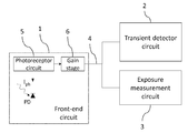
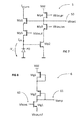
- FIG. 1 A simplified diagram of a pixel circuit according to a possible embodiment is shown in FIG. 1 .
- the pixel circuit comprises a front-end circuit 1 , a transient detector circuit 2 , and an exposure measurement circuit 3 .
- the front-end circuit 1 comprises a single photodiode PD and has an output 4 .
- the photodiode PD converts incident light into a photocurrent I ph determined by the light exposure of said single photodiode PD.
- the front-end circuit 1 also comprises a photoreceptor circuit 5 and a gain stage 6 for generating a photoreceptor signal derived from the light exposure of said single photodiode PD.
- the photoreceptor signal is delivered at the output 4 of the front-end circuit 1 in order to be exploited by both the transient detector circuit 2 and the exposure measurement circuit 3 .
- the transient detector circuit 2 is configured for detecting a change in the photoreceptor signal delivered on the front-end circuit output 4 .
- the transient detector circuit 2 continuously monitors the photoreceptor signal for changes and responds with a signal that identifies a fractional increase or decrease in the photoreceptor signal that exceeds adjustable thresholds.
- the exposure measurement circuit 3 is configured for measuring the photoreceptor signal delivered on the output 4 of the front-end circuit 1 .
- the exposure measurement cycle is initiated if the transient detector 2 circuit has detected a change in the photoreceptor signal, but it can also be initiated through an externally applied control signal independent from any change detection.
- U.S. Pat. No. 7,728,269 discloses a transient detector circuit that can be used in some embodiments of the invention. Principles of such a transient detector circuit are explained below.
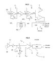
- FIG. 2 A simplified diagram of the transient detector circuit 2 for detecting changes in the photoreceptor signal is shown on FIG. 2 .
- the input signal V front at the input 20 of the transient detector circuit 2 is the photoreceptor signal V front at output 4 of the front-end circuit 1 .
- the transient detector circuit 2 comprises a first capacitor C 1 .
- One of the terminals of said first capacitor C 1 is connected to the input 20 of the transient detector circuit 2 , i.e. it is connected to the output 4 of the font-end circuit 1 .
- the other terminal of the first capacitor C 1 is connected to an amplifier Al, a second capacitor C 2 and a reset switch S RS , said amplifier A 1 , second capacitor C 2 and reset switch S RS being arranged in parallel, and connected on one end to the first capacitor C 1 and on the other end to a common node Diff.
- Capacitances and gain are chosen so as to define a self-timed, self-balancing switched-capacitor amplifier.
- Two voltage comparators 7 , 8 respectively detect upward and downward changes of the voltage V Diff at the common node Diff.
- the voltage comparators 7 , 8 have the common node Diff at their inputs, and their outputs are connected to a logic circuit 9 .
- Changes of the photoreceptor signal are amplified by the capacitively coupled inverting amplifier Al and appear as a deviation from a defined voltage level (operating point after a reset event) at the node Diff. If the signal at the common node Diff crosses certain adjustable threshold levels, this event is detected by one of two voltage comparators 7 , 8 , which sends a signal to the logic circuit 9 , and a request signal (Vreq,rel+ or Vreq,rel ⁇ , depending on the direction of the detected change) is activated by the logic circuit 9 .
- an external data receiver (not shown) sends back an acknowledge signal Vack,rel that is turned into a reset signal RST by the logic block 9 .
- the reset signal RST controls the reset switch S RS , and such an activation closes the reset switch S RS . Accordingly, the input node of the amplifier A 1 is short-circuited to its output and the operating point of the amplifier A 1 is reset. Subsequently the request signal is deactivated and the circuit is ready for detecting a new change event.
- the request signal Vreq,rel+ or Vreq,rel ⁇ is also used to generate the control signal Vres,abs sent to the exposure measurement circuit 3 to initiate an absolute exposure measurement, making this measurement conditional to the prior detection of a change in pixel illuminance, signaled by the transient circuit detector 2 .
- the entire (1 or 2-dimensional) pixel array can be initiated to execute an exposure measurement simultaneously in all pixels by an externally applied control signal.
- the request signals Vreq,rel+ and Vreq,rel ⁇ are sent to a bus arbiter (not shown) which initiates and controls the transmission of data packets.
- a bus arbiter not shown
- changes in photodiode illumination are detected and as a result, the array address of the respective pixel is transmitted with low latency over an asynchronous data bus (not shown), thereby signaling the coordinates in space and (inherently) in time of the detected change.
- the direction of change (increase or decrease) for each event is determined by which one of the two comparators detects the event.
- FIG. 3 illustrates an improvement of the transient detector circuit 2 , wherein a two-stage amplifier is used instead of the single capacitively coupled inverting amplifier whereby greatest temporal contrast sensitivity can be achieved.
- a two-stage amplifier is used instead of the single capacitively coupled inverting amplifier whereby greatest temporal contrast sensitivity can be achieved.
- the two-stage topology of single-ended inverting common-source stages with capacitive feedback, operating in the sub-threshold region and separated by a follower buffer A SF allows a significant increase in amplifier gain per unit area and leads to reduced charge injection noise (as explained below), consequently improving the temporal contrast sensitivity of the transient detector circuit.
- the first stage has a first capacitor C 1 connected by one of its terminal to the input 20 of the transient detector circuit 2 ,
- the other terminal of the first capacitor C 1 is connected to a first amplifier A 1 , a second capacitor C 2 and a first reset switch S RS1 , said first amplifier A 1 , second capacitor C 2 and first reset switch S RS being arranged in parallel, and connected on one end to the first capacitor C 1 and on the other end to a first node Diff 1 .
- the second capacitor C 2 is thus being charged by means of the photoreceptor signal at the output 4 of the front-end circuit 1 .
- the follower buffer A SF separates the two stages. It is connected on one end to the first node Diff 1 of the first stage and on the other end to a terminal of a third capacitor C 3 that belongs to the second stage.
- the other terminal of the third capacitor C 3 is connected to a second amplifier A 2 , a fourth capacitor C 4 and a second reset switch S RS2 , said second amplifier A 2 , fourth capacitor C 4 and second reset switch S RS2 being arranged in parallel, and connected on one end to the third capacitor C 3 and on the other end to a second node Diff 2 .
- the two voltage comparators 7 , 8 are connected to the second stage through the second node Diff 2 .
- the two voltage comparators 7 , 8 are threshold detectors arranged to detect if a voltage over the fourth capacitor C 4 exceeds threshold values, and if it does, a signal is sent to the control logic 9 , and a request signal (Vreq,rel+ or Vreq,rel ⁇ , depending on the direction of the detected change) is activated by the logic circuit 9 as described above).
- the charge injection in the first stage through the first reset switch S RS1 has a greater impact on the amplified signal at second node Diff 2 than a charge injection in the second stage through the second reset switch S RS2 .
- a reset control circuit RCC is thus provided, which receives the reset signal RST from the logic circuit 9 and outputs a first reset signal RST 1 controlling the first reset switch S RS1 and a second reset signal R ST2 controlling the second reset switch S RS2 .
- the first and second reset signals can thus be controlled in order to eliminate the charge injection due to the first reset switch S RS1 .
- a light exposure measurement cycle of a photodiode by means of the exposure measurement circuit 3 is usually initiated by detection, by the transient detector circuit 2 , of a change in the photoreceptor signal derived from the intensity of the incident light at the photodiode PD.
- the light exposure of the photodiode PD is measured by determining the time for a voltage across a discharging capacitor C s of the exposure measurement circuit 3 to reach at least a reference voltage.
- the measurement capacitor Cs of the exposure measurement circuit 3 is charged by a voltage corresponding to the photoreceptor signal.
- FIG. 4 shows a simplified diagram of an example of the exposure measurement circuit 3 for measuring the photoreceptor signal according to a possible embodiment of the invention.
- the exposure measurement circuit 3 comprises an input 30 connected to the output 4 of the front-end circuit 1 for receiving the photoreceptor signal.
- a measurement capacitor C S is connected by a first switch S S to the input 30 .
- a unity-gain buffer 13 may be provided at the input 30 .
- the first switch S S is configured for connecting or disconnecting the measurement capacitor Cs from the input 30 , and is controlled to this end by a measurement control signal V EM .
- the measurement control signal V EM is derived by logic block 12 from the control signal V res,abs sent by the control logic 9 of the transient detector circuit 2 upon detection of a change in the photoreceptor signal.
- the measurement capacitor C s and the first switch S S are connected through a common node S.
- the other terminal of the measurement capacitor Cs is grounded.
- a current source 10 is arranged in series with a second switch S 2 .
- the second switch S 2 is also controlled by the measurement control signal V EM and is configured for controlling a discharge of the measurement capacitor C s .
- the branch of the current source 10 is open, and thus the measurement capacitor C S cannot discharge.
- the second switch S 2 is passing (closed state)
- the branch of the current source 10 is closed, and thus the measurement capacitor C S can discharge through this branch.
- the second switch S 2 is connected to ground, or it may be connected to any current sink.
- the first and second switches may be implemented as MOS transistors. It shall be noted that for illustration purposes, the first switch S S and the second switch S 2 are both depicted in an open state at the same time, but in operation only one of them is open while the other is closed. The same applies for the switches of FIG. 5 .
- the exposure measurement circuit 3 comprises a voltage comparator 11 , having a signal input connected to one of the terminals of the measurement capacitor Cs and a reference input connected a reference voltage V ref .
- the terminal of the measurement capacitor Cs connected to the measurement comparator 11 is the common node S to which are connected the first switch S S and the current source 10 .
- the output of the voltage comparator 11 is fed to a logic circuit 12 .
- the logic circuit 12 is responsible for controlling the status of the exposure measurement cycle and for the (asynchronous) transmission of the pixel signals, and hence of the result of the exposure measurement, to an address encoder and bus arbiter (not shown).
- the instantaneous voltage V S at the common node S, to which the measurement capacitor Cs and the current source 10 are connected is used.
- the instantaneous voltage V S can be approximated as
- V s k 1 ln ( I ph )+ k 2
- I ph is the intensity of the photocurrent of the photodiode PD of the front-end circuit 1 , k 1 and k 2 are constant factors.
- the instantaneous value of the voltage V S relates logarithmically to the instantaneous photocurrent I ph , consequently a measurement of the voltage V S allows to reconstruct instantaneous photocurrent I ph , and thus to derive the light exposure level of the photodiode PD.
- Constants k 1 and k 2 depend on details of the circuit implementation as well as on individual device parameters which can vary due to non-uniform fabrication process parameters. Consequently, k 1 and k 2 may not be identical for individual pixel circuits across an array (leading to so-called fixed pattern noise, FPN).
- k 1 and k 2 are determined for each pixel individually, and their influence on the exposure measurement results are removed by calibration. Such a calibration can for example be based on a homogeneous optical stimulation of the pixel array, or on uniform electrical signal stimulation.
- the first switch S s is closed, so that the common node S is connected to the input 30 of the exposure measurement circuit 3 .
- the voltage V s at the common node S thus follows the voltage V front at the output 4 of the front-end circuit 1 .
- the voltage between the terminals of the measurement capacitor C s also follows the voltage V front at the output 4 of the front-end circuit 1 , and consequently depends on the light exposure of the photodiode PD.
- a measurement control signal V res,abs is received by the exposure measurement circuit 3 , which initiates an exposure measurement cycle.
- the first switch S s Upon activation of the control signal V res,abs , the first switch S s is opened by the measurement control signal V EM , thus disconnecting the measurement capacitor Cs from the input 30 of the exposure measurement circuit 3 . At that moment, the measurement capacitor C S is charged according to the instantaneous value of the common node voltage V S before opening the first switch S S .
- the second switch S 2 can be simultaneously closed by means of the same measurement control signal V EM , or shortly after by means of another signal that controls the second switch S 2 .
- a reference voltage V ref is applied to a reference input of the voltage comparator 11 with reference voltage V ref being chosen so that in every case the relation V ref ⁇ V S is assured.
- the signal input of the voltage comparator 11 is connected to V S . Due to the closing of the second switch S 2 , the measurement capacitor Cs is discharged by a constant current I dec controlled by the current source 10 .
- the voltage V S at the signal input of the measurement comparator 11 thus decreases, with a decreasing rate that depends on the capacitance of the measurement capacitor Cs and on the intensity of the constant current I dec imposed by the current source 10 .
- the measurement comparator 11 When the voltage V S at the signal input of the measurement comparator 11 reaches the reference voltage V ref , the measurement comparator 11 switches, i.e. it toggles its output, and an end-of-measurement signal V req,abs is activated by logic block 12 .
- the time between the active edges of the control signal V res,abs and the end-of-measurement signal V req,abs encodes the average absolute pixel exposure measure during this time, according to the relation
- V S ⁇ ( I ph ) - V ref I dec C s ⁇ T
- I dec denotes the intensity of the constant current imposed by the current source 10
- C s is the capacitance of the measurement capacitor Cs
- I ph is the intensity of the photocurrent of the photodiode PD
- T is the time needed for the voltage V s to reach the reference voltage V ref (or in other words the time between the active edges of the control signal V res,abs and the end-of-measurement signal V req,abs ).
- the intensity I ph of the photocurrent of the photodiode PD and hence the pixel light exposure can be determined.
- the exposure measurement request signals Vreq,abs are sent to a bus arbiter (not shown) which initiates and controls the transmission of data packets.
- the array address of the respective pixel is transmitted with low latency over an (asynchronous) data bus (not shown), thereby signaling the coordinates in space and—inherently—in time of the end-of-measurement, thus effectively transmitting the instantaneous pixel grey level value.
- control logic 12 can contain a digital counter device that directly digitizes the time between activation of control signal V req,abs and the exposure measurement request signals Vreq,abs.
- said transmitted data packet can contain, in addition to the pixel array address, the measured grey level digitized by the counter.
- control measurement control signal V EM With the deactivation by control logic 12 of control measurement control signal V EM , the first switch S S is closed, and the second switch S 2 is opened, so that voltage V s at the common node S can resume tracking the photocurrent signal.
- the deactivation of signal V EM is done by control logic 12 upon reception of an external acknowledge signal V ack,abs .
- a new exposure measurement cycle can be started as soon as initiated by the transient detector circuit 2 or by an external signal.
- charge injection into capacitor C s occurs while opening the first switch S s , which influences the signal voltage V s .
- the measurement capacitor should have a high enough capacitance C s , and techniques for compensation such as dummy switches and balanced transistor switches or bottom-plate transistor switches can be used.
- FIG. 5 shows a simplified diagram of an example of the exposure measurement circuit 3 for measuring the photoreceptor signal according to another possible embodiment of the invention.
- This embodiment is similar to the embodiment depicted in FIG. 4 and described above, except in that the reference input of the measurement comparator 11 is connected to the reference switch S ref instead of being directly connected to a reference voltage V ref .
- the reference switch S ref is operable to connect the reference input of the measurement comparator 11 either to a first reference voltage V ref,h or a second reference voltage V ref,l .
- the first reference voltage V ref,h is higher than the second reference voltage V ref,l .
- the reference switch S ref is controlled by the logic block 12 .
- Activation of the control signal V res,abs also resets the logic block 12 to an initial state Z 0 , and, via the logic block 12 , controls the reference switch S ref so that the first reference voltage V ref,h is selected to be applied to the reference input of the voltage comparator 11 .
- the second switch S 2 is closed and the voltage V S at the signal input of the measurement comparator 11 decreases, with a decrease rate that depends on the capacitance of the measurement capacitor Cs and on the intensity of the constant current I dec imposed by the current source 10 .
- the measurement comparator 11 switches, i.e. it toggles its output, and the first end-of measurement signal V req,absh is activated.
- the logic block 12 changes to another state Z 1 , and the reference switch S ref is switched so that the second reference voltage V ref,l is selected to be applied to the reference input of the voltage comparator 11 .
- the light exposure of the photodiode PD is measured by determining and comparing durations corresponding to the time for the voltage across the discharging capacitor C S to reach the first and second reference voltages. During a measurement cycle, a relation between the different values is:
- I dec C s V ref , h - V ref , l T ref
- the first reference voltage V ref,h and the second reference voltage V ref,l are external voltages provided to each pixel of the array. Accordingly, the voltage difference V ref,h ⁇ V ref,l is the same for every pixel of an array. As previously, with T the duration for the decreasing voltage V s to reach the first reference voltage V ref,h the following relation still holds:
- V S ⁇ ( I ph ) - V ref , h I dec C s ⁇ T
- V S ⁇ ( I ph ) - V ref , h V ref , h - V ref , l T ref ⁇ T
- both signals Vreq,absh and Vreq,absl are sent to a bus arbiter (not shown) which initiates and controls the transmission of data packets.
- the array address of the respective pixel is transmitted with low latency over an (asynchronous) data bus (not shown), thereby signaling the coordinates in space and (inherently) in time of the first and second threshold voltage crossings (signifying beginning and end of an exposure measurement, respectively), thus effectively transmitting the instantaneous pixel grey level value.
- control logic 12 can contain a digital counter device that directly digitizes the time between (activation of) signals Vreq,absh and Vreq,absl.
- Vreq,absl is sent to the bus arbiter (not shown) which initiates and controls the transmission of data packets, along with the result of said digitization.
- the transmitted data packet can contain, in addition to the pixel array address, the measured grey level digitized by the counter.
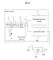
- the exposure measurement circuit 3 is constituted by a sample-and-hold circuit 100 that samples the output 4 of the front-end circuit 1 at the time of activation by the transient detector circuit 2 of control signal V res,abs .
- the output 101 of the sample-and-hold circuit 100 is connected to a pixel-external voltage analog-to-digital converter (ADC) 102 .
- ADC analog-to-digital converter
- One ADC 102 per pixel array or one ADC 102 per pixel column can be arranged.
- the output 103 of the ADC 102 is connected to a data bus (not shown).
- activation of the sample-and-hold circuit 100 is controlled by control signal V res,abs from transient detector circuit 2 .
- the sampled voltage is sent to the ADC via output 101 for analog-to-digital conversion.
- the result of the conversion along with the pixel array address is transmitted to a bus arbiter (not shown) which initiates and controls the transmission of data packets. In this way, the array address of the respective pixel and its instantaneous grey level are transmitted with low latency over an (asynchronous) data bus (not shown).
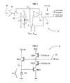
- the photoreceptor circuit 5 of the front-end circuit 1 can for example be the one described in U.S. Pat. No. 7,728,269, which is depicted in FIG. 6 .
- This circuit comprises an output 50 for delivering the photoreceptor signal derived from the light exposure of the single photodiode PD, said photoreceptor signal being constituted by a front voltage Vfront. It also comprises a first photoreceptor transistor Mp 1 having a drain and a gate, the gate of said first photoreceptor Mp 1 being connected to said output 50 .
- a second photoreceptor transistor Mp 2 has its gate connected to the photodiode PD and its source is grounded (i.e.
- the drain of the third photoreceptor transistor Mp 3 is connected to the output 50 , thus also to the gate of the first photoreceptor transistor Mp 1 .
- the drain of the third photoreceptor transistor Mp 3 is also connected to the drain of a fourth photoreceptor transistor Mp 4 , whose gate is biased by a biasing voltage Vbias,pr and whose source is connected to a high supply voltage Vdd.
- the first photoreceptor transistor Mp 1 , the second photoreceptor transistor Mp 2 and the third photoreceptor transistor Mp 3 are N-type MOSFETs, while the fourth photoreceptor transistor Mp 4 is a P-type MOSFET.
- the output voltage Vfront shows a logarithmic relation to the photocurrent I ph :
- V front n Mp ⁇ ⁇ 1 . V t . ln ⁇ ( L Mp ⁇ ⁇ 1 W Mp ⁇ ⁇ 1 ⁇ I ph I 0 , Mp ⁇ ⁇ 1 ) - V D
- a change in the photocurrent I ph from a first value I ph1 to a second value I ph2 causes a change ⁇ V front of the output voltage V front according to:
- the 3-dB frequency which corresponds to the half power point, is approximately calculated as
- C Mp1,a is the capacitance between the source of the first photoreceptor transistor Mp 1 and the output of the amplifier constituted by the second, third and fourth photoreceptor transistors Mp 2 , Mp 3 and Mp 4 , which is also the output 50 of the photoreceptor circuit 5 ,
- C D is the junction capacitance of the photodiode PD
- V t is the thermal voltage
- ⁇ is the small signal gain of the amplifier constituted by the second, third and fourth photoreceptor transistors Mp 2 , Mp 3 and Mp 4 .
- the capacitance C Mp1,a depends mainly on the gate-source overlap capacitance of the first photoreceptor transistor Mp 1 , which is proportional to its channel width.
- the 3 dB frequency of the circuit in comparison to a configuration without feedback, is no longer dominated by the capacitance of the photodiode PD, but by the much smaller gate-source overlap capacitance of the first photoreceptor transistor Mp 1 .
- FIG. 7 shows another circuit exhibiting significant improvements with respect to the gain and the bandwidth.
- the improved circuit is also a logarithmic, continuous-time photoreceptor circuit with feedback for improving the bandwidth, but compared to the photoreceptor circuit of FIG. 6 , an additional fifth photoreceptor transistor Mp 5 is arranged between the photodiode PD and the first photoreceptor transistor Mp 1 .
- the improved photoreceptor circuit 5 of FIG. 7 comprises an output 50 for delivering the photoreceptor signal derived from the light exposure of said single photodiode, said photoreceptor signal being constituted by a voltage Vfront. It comprises a first photoreceptor transistor Mp 1 having a drain and a gate, the gate of said first photoreceptor Mp 1 being connected to said output 50 . It also comprises a fifth photoreceptor transistor Mp 5 having a drain, a source and a gate, the source of said fifth photoreceptor transistor Mp 5 being connected to the single photodiode PD and the gate of fifth photoreceptor transistor Mp 5 being biased by a biasing voltage Vbias,d.
- the first photoreceptor transistor Mp 1 and the fifth photoreceptor transistor Mp 5 have a common source.
- a second photoreceptor transistor Mp 2 has its gate connected to the photodiode PD and to the drain of the fifth photoreceptor transistor Mp 5 . Its source is grounded (i.e. connected to a low supply voltage) while its drain is connected to the source of a third photoreceptor transistor Mp 3 , whose gate is biased by a biasing voltage Vbias,cas. The drain of the third photoreceptor transistor Mp 3 is connected to the output 50 , thus also to the gate of the first photoreceptor transistor Mp 1 .
- the drain of the third photoreceptor transistor Mp 3 is also connected to the drain of a fourth photoreceptor transistor Mp 4 , whose gate is biased by a biasing voltage Vbias,pr and whose source is connected to a high supply voltage Vdd.
- the first photoreceptor transistor Mp 1 , the second photoreceptor transistor Mp 2 and the third photoreceptor transistor Mp 3 are N-type MOSFET, while the fifth photoreceptor transistor Mp 5 and the fourth photoreceptor transistor Mp 4 are P-type MOSFET.
- the output voltage V front of the circuit of FIG. 6 still depends logarithmically on the photocurrent intensity I ph :
- V front n Mp ⁇ ⁇ 1 . V t . ln ⁇ ( L Mp ⁇ ⁇ 1 W Mp ⁇ ⁇ 1 ⁇ I ph I 0 , Mp ⁇ ⁇ 1 ) + n Mp ⁇ ⁇ 5 . V t . ln ⁇ ( L Mp ⁇ ⁇ 5 W Mp ⁇ ⁇ 5 ⁇ I ph I 0 , Mp ⁇ ⁇ 5 ) + V bias , d
- n Mp5 being the sub-threshold slope factor of the fifth photoreceptor transistor Mp 5 ,
- L Mp5 is the channel length of the first photoreceptor transistor Mp 5 .
- W Mp5 is the channel width of the first photoreceptor transistor Mp 5 .
- I 0,Mp5 is the sub-threshold saturation current of the first photoreceptor transistor Mp 5 .
- V bias the biasing voltage applied to the gate of the fifth photoreceptor transistor Mp 5 .
- a change in the photocurrent I ph from a first value I ph1 to a second value I ph2 causes a change ⁇ V front of the output voltage V front according to:
- V front n Mp ⁇ ⁇ 1 . V t . ln ⁇ ( I ph ⁇ 2 I ph ⁇ 1 ) + n Mp ⁇ ⁇ 5 . V t . ln ⁇ ( I ph ⁇ 2 I ph ⁇ 1 )
- the gain is doubled with respect to the photoreceptor circuit of FIG. 6 .
- the increased gain achieved by the photoreceptor circuit of FIG. 7 allows for smaller current intensity changes ⁇ I ph of the photocurrent I ph to be detected since in response to a certain change ⁇ I ph in the intensity of the photocurrent I ph , the resulting voltage change is increased by a doubled gain. Further, since the resulting voltage change is increased before the input of a following amplifier, such as the switched-capacitor differencing amplifier of the transient detector circuit 3 , the gain of such a following amplifier can be smaller while achieving the same overall temporal contrast (i.e. relative change) sensitivity, leading to a significant reduction of the CMOS device size, especially the capacitor size of a switched-capacitor amplifier.
- the 3-dB frequency which corresponds to the half power point, is approximately calculated as
- C Mp5,DS is the drain-source coupling capacitance of the fifth transistor Mp 5 .
- this capacitance is significantly smaller than the gate-source overlap capacitance C Mp1 of the first photoreceptor transistor Mp 1 that used to determine the 3-dB frequency in the circuit of FIG. 6 .
- the bandwidth is therefore increased by the ratio C Mp5,DS /C Mp1 .
- the response delay of the transient detector circuit 2 is significantly reduced, and the temporal resolution of the pixel circuit and thus of the sensor device is improved.
- the gate of the fifth photoreceptor transistor Mp 5 can be connected to its source instead of being driven by a biasing voltage Vbias,d. In this configuration however, while the voltage gain is still doubled, there is no increase of the bandwidth.
- FIG. 8 shows a simplified diagram of an example of a pre-amplifier gain stage 6 for amplifying the signal Vfront at the output of the photoreceptor circuit 5 , instead of a conventional follower buffer.
- the pre-amplifier gain stage 6 comprises an input connected to the output of the photoreceptor circuit 5 for receiving the photoreceptor signal Vfront, and an output connected both to the input of the transient detector circuit 2 and to the input of the exposure measurement circuit 3 , for delivering the amplified photoreceptor signal Vamp.
- the pre-amplifier gain stage 6 comprises a first gain transistor Mg 1 having a drain, a source and a gate.
- the gate of the first gain transistor Mg 1 is connected to the input of the gain stage, i.e. to the output of the photoreceptor circuit 5 .
- the source of the first gain transistor Mg 1 is connected to a reference biasing voltage Vbias,ref and the drain of said first gain transistor Mg 1 is connected to the output of the gain stage.
- the first gain transistor Mg 1 is an N-channel type MOS transistor.
- the pre-amplifier gain stage 6 also comprises a plurality of gain transistors Mg 2 , Mgk in series, each one of these gain transistor Mg 2 , Mgk having a drain, a source and a gate, and each one of these gain transistors Mg 2 , Mgk in series having its drain connected to its gate (diode-connected transistors).
- One of these gain transistors in series has its drain connected to the drain of the first gain transistor Mg 1 and is referred to as Mg 2 . Accordingly, this gain transistor Mg 2 has its gate connected to the output of the gain stage 6 .
- the gain transistors in series are P-channel type MOS transistors.
- the described gain stage 6 is a common-source amplifier, the first gain transistor Mg 1 being an N-MOS input transistor and the series of diode-connected P-MOS gain transistors Mg 2 , Mgk being a load.
- the first gain transistor Mg 1 being an N-MOS input transistor
- the series of diode-connected P-MOS gain transistors Mg 2 , Mgk being a load.
- Such a structure with diode-connected load has a gain which is not strongly dependent on dimensions, so that dimension-related mismatch influence is reduced, which improve fixed-pattern noise (FPN) performance of the pixel array.
- FPN fixed-pattern noise
- more diode-connected gain transistors are arranged in series.
- three or four diode-connected gain transistors are connected in series.
- the maximum number of such diode-connected gain transistors are arranged in series is determined by the input voltage swing, i.e. the expected upper level of the input voltage Vfront such that the gate-source voltage across the series of diode-connected transistors Mg 2 to Mgk is not limited by the resulting output voltage Vamp.
- the output voltage V amp is calculated as follows:
- V amp V DD - ( k - 1 ) . n Mg ⁇ ⁇ 2 . V t . ln ⁇ ( L Mg ⁇ ⁇ 2 W Mg ⁇ ⁇ 2 ⁇ W Mg ⁇ ⁇ 1 L Mg ⁇ ⁇ 1 ⁇ I 0 , Mg ⁇ ⁇ 1 I 0 , Mg ⁇ ⁇ 2 ) - ( k - 1 ) . n Mg ⁇ ⁇ 2 n Mg ⁇ ⁇ 1 ⁇ ( V front - V bias , ref )
- V DD is the high supply voltage
- n Mg1 and n Mg2 are the sub-threshold slope factors of the gain transistors Mg 1 and Mg 2 , respectively,
- V t is the thermal voltage
- L Mg1 and L Mg2 are the channel lengths of the first gain transistor Mg 1 and of the second gain transistors Mg 2 , respectively,
- W Mg1 and W Mg2 are the channel widths of the first gain transistor Mg 1 and of the second gain transistors Mg 2 , respectively,
- I 0,Mg1 and I 0,Mg2 are the sub-threshold saturation currents of the first gain transistor Mg 1 and of the second gain transistors Mg 2 , respectively.
- An input voltage change ⁇ V front results in an output voltage change ⁇ V amp of:
- ⁇ ⁇ ⁇ V amp - ( k - 1 ) ⁇ n Mg ⁇ ⁇ 2 n Mg ⁇ ⁇ 1 ⁇ ⁇ ⁇ ⁇ V front
- the gain thus provided by the gain stage 6 allows for smaller current intensity changes ⁇ I ph of the photocurrent I ph to be detected since in response to a certain change ⁇ I ph in the intensity of the photocurrent I ph , the resulting voltage change is increased by a (k-1)-fold gain. Further, since the resulting voltage change is increased before the input of a following amplifier, such as the switched-capacitor differencing amplifier of the transient detector circuit 3 , the gain of such a following amplifier can be smaller while achieving the same overall contrast sensitivity, leading to a significant reduction of the CMOS device size, especially the capacitor size of a switched-capacitor amplifier.
- a photocurrent-dependent bandwidth limitation can be achieved.
- the gain stage then provides an automatic, photocurrent-controlled noise reduction by self-adjusting its bandwidth.
- the 3 dB frequency which corresponds to the half power point, is proportional to the current I Mg1 flowing through the first gain transistor Mg 1 :
- the 3 dB frequency is proportional to:
- the biasing reference voltage V bias,ref can be derived globally for all pixels in an array using a dummy circuit with a covered photodiode in a photoreceptor circuit such as the one of FIG. 6 or 7 , with the output voltage of such a photoreceptor circuit used as the biasing reference voltage V bias,ref .
- the gain stage circuit 6 can thus replace a conventional source follower for effectively decoupling the sensitive front-end circuit 1 from the subsequent circuits, i.e. the transient detector circuit 2 and the exposure measurement circuit 3 , and photocurrent-dependent bandwidth control and additional signal amplification can be achieved.
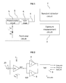
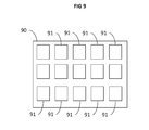
- FIG. 9 shows an image sensor 90 comprising a plurality of pixel circuits 91 according to possible embodiments of the invention as described above.
- the depicted pixel circuits 91 are arranged in an array.
Landscapes
- Engineering & Computer Science (AREA)
- Multimedia (AREA)
- Signal Processing (AREA)
- Transforming Light Signals Into Electric Signals (AREA)
- Computer Vision & Pattern Recognition (AREA)
- Solid State Image Pick-Up Elements (AREA)
Abstract
-
- a front-end circuit comprising a single photodiode and having an output, said front-end circuit being configured for delivering on said output a photoreceptor signal derived from a light exposure of said single photodiode;
- a transient detector circuit configured for detecting a change in said photoreceptor signal delivered on said output;
- an exposure measurement circuit configured for measuring said photoreceptor signal delivered on said output upon detection by the transient detector circuit of a change in the photoreceptor signal.
Description
- The invention relates to a pixel circuit for an image sensor. More specifically, it relates to a pixel circuit and an operating method thereof, wherein an exposure measurement circuit is configured for measuring the light exposure intensity from a photoreceptor signal derived from a light exposure of a single photoreceptor, upon detection by a transient detector circuit of a change in said photoreceptor signal.
- Conventional image sensors acquire the visual information time-quantized at a predetermined frame rate. Each frame carries the information from all pixels, regardless of whether or not this information has changed since the last frame has been acquired. This approach obviously results, depending on the dynamic contents of the scene, in a more or less high degree of redundancy in the recorded image data. The problem worsens as modern image sensors advance to ever higher spatial and temporal resolution. The hardware required for post-processing of the data increases in complexity and cost, demand on transmission bandwidth and data storage capacity surges and the power consumption rises, leading to severe limitations in all kinds of vision applications, from demanding high-speed industrial vision systems to mobile, battery-powered consumer devices.
- One approach to dealing with temporal redundancy in video data is frame difference encoding. This simplest form of video compression includes transmitting only pixel values that exceed a defined intensity change threshold from frame to frame after an initial key-frame. Known frame differencing imagers rely on acquisition and processing of full frames of image data and are not able to self-consistently suppress temporal redundancy and provide real-time compressed video output. Furthermore, even when the processing and difference quantization is done at the pixel-level, the temporal resolution of the acquisition of the scene dynamics, as in all frame-based imaging devices, is still limited to the achievable frame rate and is time-quantized to this frame rate.
- The adverse effects of data redundancy are most effectively avoided by not recording the redundant data in the first place and directly reducing data volume at the sensor output level. The immediate benefits are reductions in bandwidth, memory and computing power requirements for data transmission and post-processing, hence decreasing system power, complexity and cost. In addition, the frame-based, clocked principle of operation of conventional CMOS or CCD image sensors leads to limitations in temporal resolution as scene dynamics are quantized to the frame rate at which the pixel field of view is read out, and poor dynamic range.
- The problem to be solved by the present invention is to provide a method and an apparatus for the continuous acquisition of the full visual information of an observed dynamic scene with high temporal and intensity resolution, over a wide dynamic range (of recordable and processable light intensity) and thereby generating the minimum necessary amount of data volume. Thus, the generated data are not constituted by a succession of frames containing the image information of all pixels, but an (asynchronous) stream of change and intensity (i.e. grey level) information of individual pixels, which are recorded and transmitted only if an actual change in light intensity in the field of view of the individual pixel has been detected by the pixel itself.
- This method leads to a substantial reduction of generated data through complete suppression of the temporal redundancy in the picture information that is typical for conventional image sensors, though with the data containing the same, or even higher, information content. The picture element for an image sensor that implements the aforementioned method as well as the required asynchronous data readout mechanism can be realized on basis of analogue electronic circuits. An image sensor with a multiplicity of such picture elements is typically realized and fabricated as an integrated system-on-chip e.g. in CMOS technology.
- Implementing such a sensor and thus avoiding the above mentioned drawbacks of conventional image data acquisition would be beneficial for a wide range of artificial vision applications including industrial high-speed vision (e.g. fast object recognition, motion detection and analysis, object tracking, etc.), automotive (e.g. real-time 3D stereo vision for collision warning and avoidance, intelligent rear-view mirrors, etc.), surveillance and security (scene surveillance) or robotics (autonomous navigation, SLAM) as well as biomedical and scientific imaging applications. As the sensor operation is inspired by working principles of the human retina, one advantageous example application is the treatment of a degenerated retina of a blind patient with an implantable prosthesis device based on the data delivered by such a sensor.
- A solution for achieving the aforementioned complete temporal redundancy suppression is based on pixel-individual pre-processing and acquiring of the image information, event-controlled (i.e. independently of external timing control such as clock, shutter or reset signals) and conditionally (i.e. only when changes in the scene have been detected). As explained below, the control of the image data acquisition is transferred to the pixel-level and can be done at very high temporal resolution (e.g. fully asynchronously).
- In the case of the optical transient sensor, or dynamic vision sensor (DVS), changes in lighting intensity received by the individual, autonomously operating pixels are detected by an electronic circuit, “a transient detector”, described in patent U.S. Pat. No. 7,728,269.
- U.S. patent application US 2010/0182468 A1 discloses combining transient detector circuits, i.e. light exposure intensity changes detector circuits, and conditional exposure measurement circuits. A transient detector circuit individually and asynchronously initiates the measurement of a new exposure measure only if—and immediately after—a brightness change of a certain magnitude has been detected in the field-of-view of a pixel. Such a pixel does not rely on external timing signals and independently requests access to an (asynchronous and arbitrated) output channel only when it has a new grayscale value to communicate. Consequently, a pixel that is not stimulated visually does not produce output. In addition, the asynchronous operation avoids the time quantization of frame-based acquisition and scanning readout.
- For each pixel, the transient detector circuit monitors a photoreceptor voltage derived from a first photodiode for detecting relative voltage changes that exceed a threshold. Upon such detection, the transient detector circuit outputs a command for the exposure measurement circuit of the same pixel to start an absolute intensity measurement, i.e. an absolute grey level measurement. The exposure measurement circuit uses a second photodiode of the pixel, placed adjacent to the first photodiode, and derives its measure from the time duration for discharging the photodiode junction capacitance with the instantaneous photocurrent.
- However, the pixel circuit disclosed in US 2010/0182468 A1 is not optimal since it consumes a large area for a pixel element and thus cannot achieve high resolution. Furthermore, time-based exposure measurement through direct photocurrent integration often leads to a prohibitively long measurement time of a new exposure value, especially at low pixel illuminance levels, due to the corresponding small photocurrents. Finally using two separate photodiodes for change detection and exposure measurement leads to spatial divergence and motion direction dependency of the image data acquisition process, resulting in a reduction in imaging quality.
- The invention aims at providing a pixel circuit with smaller area requirements, allowing for larger array sizes or smaller sensor chip dimensions. The invention also aims at speeding up the individual measurement processes and consequently increasing temporal resolution. Furthermore, the invention aims at avoiding spatial divergence between change detection and exposure measurement caused by a use of two separate photodiodes, improving measurement accuracy and consequently image quality.
- In this respect, the invention relates to a pixel circuit comprising:
-
- a front-end circuit comprising a single photodiode and having an output, said front-end circuit being configured for delivering on said output a photoreceptor signal derived from a light exposure of said single photodiode;
- a transient detector circuit configured for detecting a change in said photoreceptor signal delivered on said output;
- an exposure measurement circuit configured for measuring said photoreceptor signal delivered on said output upon detection by the transient detector circuit of a change in the photoreceptor signal.
- In contrast to the prior art circuits wherein exposure changes were detected on a photodiode and exposure measurements were made on another photodiode, the proposed pixel circuit requires only one photodiode per pixel. Accordingly, the surface consumption of the pixel element can be reduced significantly, allowing for larger array sizes or smaller sensor chip dimensions. Resolution can also be increased. Also, the spatial divergence between change detection and exposure measurement is avoided, improving measurement accuracy and consequently image quality. Very advantageously, the duration of a grey level measurement can be significantly reduced as explained below, significantly improving the temporal resolution of the image data acquisition process.
- Other preferred, although non limitative, aspects of the pixel circuit are as follows, isolated or in a technically feasible combination:
-
- the exposure measurement circuit comprises
- an input connected to the output of the front-end circuit for receiving the photoreceptor signal,
- a capacitor connected by a first switch to said input, said first switch being configured for disconnecting said capacitor from said input,
- a source current in series with a second switch, parallel to said capacitor, said second switch being configured for controlling a discharge of said capacitor;
- the exposure measurement circuit comprises a voltage comparator having a signal input connected to one of the terminal of the capacitor and a reference input connected to a reference voltage;
- the voltage comparator has:
-
- a signal input connected to one of the terminal of the capacitor and
- a reference input connected to reference switch configured for selectively connecting said reference input to at least two reference voltages;
- the transient detector circuit comprises an amplifier having two single-ended inverting common-source stages with capacitive feedback separated by a follower buffer wherein a first capacitor is charged by means of the photoreceptor signal, and at least one threshold detector is arranged to detect if a voltage over another capacitor exceeds a threshold value;
- the front-end circuit comprises a photoreceptor circuit connected to the single diode, the photoreceptor circuit comprises:
-
- an output for delivering the photoreceptor signal derived from the light exposure of said single photodiode,
- a first photoreceptor transistor having a drain and a gate, the gate of said first photoreceptor transistor being connected to said output,
- an additional photoreceptor transistor having a drain, a source and a gate, the source of said additional photoreceptor transistor being connected to said single photodiode and,
- wherein said first and additional photoreceptor transistors have a common source;
- the gate of additional photoreceptor transistor is biased by a biasing voltage or is connected to the common source of the first and additional photoreceptor transistors;
- the front-end circuit further comprises a gain stage for amplifying the photoreceptor signal delivered on the output of the front-end circuit, said gain stage comprising:
-
- an input connected to the output of a photoreceptor circuit,
- an output,
- a first gain transistor having a drain, a source and a gate, the gate of the first gain transistor being connected to the input of the gain stage, the source of the first gain transistor being connected to a biasing voltage and the drain of said first gain transistor being connected to the output of said gain stage, and
- a plurality of gain transistors in series, each gain transistor of the series having a drain, a source and a gate, each gain transistors of the series having its drain connected to its gate, and one of said plurality of gain transistors in series having its drain connected to the drain of the first gain transistor.
- The invention also relates to an image sensor comprising a plurality of pixel circuits according to a possible embodiment of the invention.
- The invention also relates to a method for operating a pixel circuit according to one of the possible embodiment of the invention, wherein a light exposure measurement cycle of a photodiode by means of the exposure measurement circuit is initiated by detection by the transient detector circuit of a change in the photoreceptor signal derived from the intensity of the incident light at said photodiode.
- Other preferred, although non limitative, aspects of the pixel circuit are as follows, isolated or in a technically feasible combination:
-
- a light exposure measurement cycle of a photodiode by means of the exposure measurement circuit can also be initiated through an externally applied control signal independent from any detection in the photoreceptor signal derived from the intensity of the incident light at said photodiode;
- the light exposure of the photodiode is measured by determining the time for the voltage across a discharging capacitor of the exposure measurement circuit to reach at least one reference voltage;
- there is a first reference voltage and a second reference voltage, said first reference voltage being higher than said second reference voltage, and wherein the light exposure of the photodiode is measured by determining and comparing:
- a first duration corresponding to the time for the voltage across a discharging capacitor of the exposure measurement circuit to reach said first reference voltage, and
- a second duration corresponding to the time for the voltage across said discharging capacitor of the exposure measurement circuit to reach said second reference voltage;
- before the exposure measurement cycle, the capacitor of the exposure measurement circuit is charged by a voltage corresponding to the photoreceptor signal;
- the exposure measurement circuit comprises:
- an input connected to the output of the front-end circuit for receiving the photoreceptor signal,
- a capacitor connected by a first switch to said input, said first switch being configured for disconnecting said capacitor from said input,
- a source current in series with a second switch, parallel to said capacitor, said second switch being configured for controlling a discharge of said capacitor,
- and the exposure measurement cycle comprises at least the following steps:
- opening a first switch for disconnecting the measurement capacitor from the input of the measurement exposure circuit,
- closing the second switch for allowing the discharge of the capacitor,
- determining the time for the discharging capacitor of the exposure to reach at least one reference voltage,
- determining the light exposure of the photodiode from the determined discharging time of the capacitor.
- Other aspects, objects and advantages of the present invention will become better apparent upon reading the following detailed description of preferred embodiments thereof, given as non-limiting examples, and made with reference to the appended drawings wherein:
-
FIG. 1 shows a block diagram of a pixel circuit according to a possible embodiment of the invention, -
FIGS. 2 and 3 show simplified diagrams of exemplary embodiments of transient detector circuits for detecting changes in the photoreceptor signal; -
FIGS. 4 and 5 show simplified diagrams of exemplary embodiments of the exposure measurement circuit for measuring the photoreceptor signal; -
FIGS. 6 and 7 show simplified diagrams of exemplary embodiments of photoreceptor circuits; -
FIG. 8 shows a simplified diagram of a gain stage for amplifying changes in the photoreceptor signal prior to its exploitation by the transient detector circuit and by the exposure measurement circuit; -
FIG. 9 shows an image sensor comprising a plurality of pixel circuits according to the invention. -
FIG. 10 shows an alternative block diagram of a pixel circuit according to a possible embodiment of the invention, connected to a pixel-external analog-to-digital converter. - In all figures, the same reference characters refer to the same elements.
- A simplified diagram of a pixel circuit according to a possible embodiment is shown in
FIG. 1 . The pixel circuit comprises a front-end circuit 1, atransient detector circuit 2, and anexposure measurement circuit 3. The front-end circuit 1 comprises a single photodiode PD and has anoutput 4. The photodiode PD converts incident light into a photocurrent Iph determined by the light exposure of said single photodiode PD. The front-end circuit 1 also comprises aphotoreceptor circuit 5 and again stage 6 for generating a photoreceptor signal derived from the light exposure of said single photodiode PD. The photoreceptor signal is delivered at theoutput 4 of the front-end circuit 1 in order to be exploited by both thetransient detector circuit 2 and theexposure measurement circuit 3. - The
transient detector circuit 2 is configured for detecting a change in the photoreceptor signal delivered on the front-end circuit output 4. Thetransient detector circuit 2 continuously monitors the photoreceptor signal for changes and responds with a signal that identifies a fractional increase or decrease in the photoreceptor signal that exceeds adjustable thresholds. - The
exposure measurement circuit 3 is configured for measuring the photoreceptor signal delivered on theoutput 4 of the front-end circuit 1. The exposure measurement cycle is initiated if thetransient detector 2 circuit has detected a change in the photoreceptor signal, but it can also be initiated through an externally applied control signal independent from any change detection. - U.S. Pat. No. 7,728,269 discloses a transient detector circuit that can be used in some embodiments of the invention. Principles of such a transient detector circuit are explained below.
- A simplified diagram of the
transient detector circuit 2 for detecting changes in the photoreceptor signal is shown onFIG. 2 . The input signal Vfront at theinput 20 of thetransient detector circuit 2 is the photoreceptor signal Vfront atoutput 4 of the front-end circuit 1. Thetransient detector circuit 2 comprises a first capacitor C1. One of the terminals of said first capacitor C1 is connected to theinput 20 of thetransient detector circuit 2, i.e. it is connected to theoutput 4 of the font-end circuit 1. The other terminal of the first capacitor C1 is connected to an amplifier Al, a second capacitor C2 and a reset switch SRS, said amplifier A1, second capacitor C2 and reset switch SRS being arranged in parallel, and connected on one end to the first capacitor C1 and on the other end to a common node Diff. Capacitances and gain are chosen so as to define a self-timed, self-balancing switched-capacitor amplifier. Twovoltage comparators voltage comparators - Changes of the photoreceptor signal are amplified by the capacitively coupled inverting amplifier Al and appear as a deviation from a defined voltage level (operating point after a reset event) at the node Diff. If the signal at the common node Diff crosses certain adjustable threshold levels, this event is detected by one of two
voltage comparators - Upon receiving the request signal, Vreq,rel+or Vreq,rel−, and retrieving associated pixel data (see below), an external data receiver (not shown) sends back an acknowledge signal Vack,rel that is turned into a reset signal RST by the logic block 9. The reset signal RST controls the reset switch SRS, and such an activation closes the reset switch SRS. Accordingly, the input node of the amplifier A1 is short-circuited to its output and the operating point of the amplifier A1 is reset. Subsequently the request signal is deactivated and the circuit is ready for detecting a new change event.
- The request signal Vreq,rel+ or Vreq,rel− is also used to generate the control signal Vres,abs sent to the
exposure measurement circuit 3 to initiate an absolute exposure measurement, making this measurement conditional to the prior detection of a change in pixel illuminance, signaled by thetransient circuit detector 2. Alternatively, the entire (1 or 2-dimensional) pixel array can be initiated to execute an exposure measurement simultaneously in all pixels by an externally applied control signal. - The request signals Vreq,rel+ and Vreq,rel− are sent to a bus arbiter (not shown) which initiates and controls the transmission of data packets. In this way changes in photodiode illumination are detected and as a result, the array address of the respective pixel is transmitted with low latency over an asynchronous data bus (not shown), thereby signaling the coordinates in space and (inherently) in time of the detected change. The direction of change (increase or decrease) for each event is determined by which one of the two comparators detects the event.
-
FIG. 3 illustrates an improvement of thetransient detector circuit 2, wherein a two-stage amplifier is used instead of the single capacitively coupled inverting amplifier whereby greatest temporal contrast sensitivity can be achieved. Such a structure is disclosed in the article of C. Posch, D. Matolin and R. Wohlgenannt, “A Two-Stage Capacitive-Feedback Differencing Amplifier for Temporal Contrast IR Sensors”, Analog Integrated Circuits and Signal Processing Journal, vol. 64, no. 1, pp. 45-54, 2010. - The two-stage topology of single-ended inverting common-source stages with capacitive feedback, operating in the sub-threshold region and separated by a follower buffer ASF, allows a significant increase in amplifier gain per unit area and leads to reduced charge injection noise (as explained below), consequently improving the temporal contrast sensitivity of the transient detector circuit.
- The first stage has a first capacitor C1 connected by one of its terminal to the
input 20 of thetransient detector circuit 2, - The other terminal of the first capacitor C1 is connected to a first amplifier A1, a second capacitor C2 and a first reset switch SRS1, said first amplifier A1, second capacitor C2 and first reset switch SRS being arranged in parallel, and connected on one end to the first capacitor C1 and on the other end to a first node Diff1. The second capacitor C2 is thus being charged by means of the photoreceptor signal at the
output 4 of the front-end circuit 1. - The follower buffer ASF separates the two stages. It is connected on one end to the first node Diff1 of the first stage and on the other end to a terminal of a third capacitor C3 that belongs to the second stage. The other terminal of the third capacitor C3 is connected to a second amplifier A2, a fourth capacitor C4 and a second reset switch SRS2, said second amplifier A2, fourth capacitor C4 and second reset switch SRS2 being arranged in parallel, and connected on one end to the third capacitor C3 and on the other end to a second node Diff2. The two
voltage comparators voltage comparators - With both amplifier stages having similar gain, the charge injection in the first stage through the first reset switch SRS1 has a greater impact on the amplified signal at second node Diff2 than a charge injection in the second stage through the second reset switch SRS2. To eliminate the effect of the charge injection of the first reset switch SRS1, it is sufficient to guarantee that the second stage is turned on sufficiently after the first stage. This is achieved by appropriately delaying the switching of the second reset switch SRS2 with respect to the first reset switch SRS1.
- A reset control circuit RCC is thus provided, which receives the reset signal RST from the logic circuit 9 and outputs a first reset signal RST1 controlling the first reset switch SRS1 and a second reset signal RST2 controlling the second reset switch SRS2. The first and second reset signals can thus be controlled in order to eliminate the charge injection due to the first reset switch SRS1.
- A light exposure measurement cycle of a photodiode by means of the
exposure measurement circuit 3 is usually initiated by detection, by thetransient detector circuit 2, of a change in the photoreceptor signal derived from the intensity of the incident light at the photodiode PD. The light exposure of the photodiode PD is measured by determining the time for a voltage across a discharging capacitor Cs of theexposure measurement circuit 3 to reach at least a reference voltage. Before the exposure measurement cycle, the measurement capacitor Cs of theexposure measurement circuit 3 is charged by a voltage corresponding to the photoreceptor signal. -
FIG. 4 shows a simplified diagram of an example of theexposure measurement circuit 3 for measuring the photoreceptor signal according to a possible embodiment of the invention. Theexposure measurement circuit 3 comprises aninput 30 connected to theoutput 4 of the front-end circuit 1 for receiving the photoreceptor signal. A measurement capacitor CS is connected by a first switch SS to theinput 30. A unity-gain buffer 13 may be provided at theinput 30. The first switch SS is configured for connecting or disconnecting the measurement capacitor Cs from theinput 30, and is controlled to this end by a measurement control signal VEM. The measurement control signal VEM is derived bylogic block 12 from the control signal Vres,abs sent by the control logic 9 of thetransient detector circuit 2 upon detection of a change in the photoreceptor signal. - The measurement capacitor Cs and the first switch SS are connected through a common node S. The other terminal of the measurement capacitor Cs is grounded. In parallel to the measurement capacitor Cs, a
current source 10 is arranged in series with a second switch S2.The second switch S2 is also controlled by the measurement control signal VEM and is configured for controlling a discharge of the measurement capacitor Cs. When the second switch S2 is not passing (open state), the branch of thecurrent source 10 is open, and thus the measurement capacitor CS cannot discharge. When the second switch S2 is passing (closed state), the branch of thecurrent source 10 is closed, and thus the measurement capacitor CS can discharge through this branch. The second switch S2 is connected to ground, or it may be connected to any current sink. The first and second switches may be implemented as MOS transistors. It shall be noted that for illustration purposes, the first switch SS and the second switch S2 are both depicted in an open state at the same time, but in operation only one of them is open while the other is closed. The same applies for the switches ofFIG. 5 . - The
exposure measurement circuit 3 comprises avoltage comparator 11, having a signal input connected to one of the terminals of the measurement capacitor Cs and a reference input connected a reference voltage Vref. The terminal of the measurement capacitor Cs connected to themeasurement comparator 11 is the common node S to which are connected the first switch SS and thecurrent source 10. The output of thevoltage comparator 11 is fed to alogic circuit 12. Thelogic circuit 12 is responsible for controlling the status of the exposure measurement cycle and for the (asynchronous) transmission of the pixel signals, and hence of the result of the exposure measurement, to an address encoder and bus arbiter (not shown). - For exposure measurement, the instantaneous voltage VS at the common node S, to which the measurement capacitor Cs and the
current source 10 are connected, is used. The instantaneous voltage VS can be approximated as -
V s =k 1 ln(I ph)+k 2 - wherein Iph is the intensity of the photocurrent of the photodiode PD of the front-
end circuit 1, k1 and k2 are constant factors. The instantaneous value of the voltage VS relates logarithmically to the instantaneous photocurrent Iph, consequently a measurement of the voltage VS allows to reconstruct instantaneous photocurrent Iph, and thus to derive the light exposure level of the photodiode PD. - Constants k1 and k2 depend on details of the circuit implementation as well as on individual device parameters which can vary due to non-uniform fabrication process parameters. Consequently, k1 and k2 may not be identical for individual pixel circuits across an array (leading to so-called fixed pattern noise, FPN). Preferably, k1 and k2 are determined for each pixel individually, and their influence on the exposure measurement results are removed by calibration. Such a calibration can for example be based on a homogeneous optical stimulation of the pixel array, or on uniform electrical signal stimulation.
- Before the initiation of an exposure measurement cycle, the first switch Ss is closed, so that the common node S is connected to the
input 30 of theexposure measurement circuit 3. The voltage Vs at the common node S thus follows the voltage Vfront at theoutput 4 of the front-end circuit 1. The voltage between the terminals of the measurement capacitor Cs also follows the voltage Vfront at theoutput 4 of the front-end circuit 1, and consequently depends on the light exposure of the photodiode PD. - After the
transient detector circuit 2 has detected a relative change in illumination, a measurement control signal Vres,abs is received by theexposure measurement circuit 3, which initiates an exposure measurement cycle. - Upon activation of the control signal Vres,abs, the first switch Ss is opened by the measurement control signal VEM, thus disconnecting the measurement capacitor Cs from the
input 30 of theexposure measurement circuit 3. At that moment, the measurement capacitor CS is charged according to the instantaneous value of the common node voltage VS before opening the first switch SS. The second switch S2 can be simultaneously closed by means of the same measurement control signal VEM, or shortly after by means of another signal that controls the second switch S2. - A reference voltage Vref is applied to a reference input of the
voltage comparator 11 with reference voltage Vref being chosen so that in every case the relation Vref<VS is assured. The signal input of thevoltage comparator 11 is connected to VS. Due to the closing of the second switch S2, the measurement capacitor Cs is discharged by a constant current Idec controlled by thecurrent source 10. The voltage VS at the signal input of themeasurement comparator 11 thus decreases, with a decreasing rate that depends on the capacitance of the measurement capacitor Cs and on the intensity of the constant current Idec imposed by thecurrent source 10. - When the voltage VS at the signal input of the
measurement comparator 11 reaches the reference voltage Vref, themeasurement comparator 11 switches, i.e. it toggles its output, and an end-of-measurement signal Vreq,abs is activated bylogic block 12. The time between the active edges of the control signal Vres,abs and the end-of-measurement signal Vreq,abs encodes the average absolute pixel exposure measure during this time, according to the relation -
- where Idec denotes the intensity of the constant current imposed by the
current source 10, Cs is the capacitance of the measurement capacitor Cs, Iph is the intensity of the photocurrent of the photodiode PD, and T is the time needed for the voltage Vs to reach the reference voltage Vref (or in other words the time between the active edges of the control signal Vres,abs and the end-of-measurement signal Vreq,abs). From this relation, and due to the fact that -
V s k 1 ln(I ph)+k 2, - the intensity Iph of the photocurrent of the photodiode PD and hence the pixel light exposure can be determined.
- Similar to the request signals (Vreq,rel+ and Vreq,rel−) derived from the change detection events, the exposure measurement request signals Vreq,abs are sent to a bus arbiter (not shown) which initiates and controls the transmission of data packets. In this way, the array address of the respective pixel is transmitted with low latency over an (asynchronous) data bus (not shown), thereby signaling the coordinates in space and—inherently—in time of the end-of-measurement, thus effectively transmitting the instantaneous pixel grey level value.
- Alternatively,
control logic 12 can contain a digital counter device that directly digitizes the time between activation of control signal Vreq,abs and the exposure measurement request signals Vreq,abs. In this case, said transmitted data packet can contain, in addition to the pixel array address, the measured grey level digitized by the counter. - With the deactivation by
control logic 12 of control measurement control signal VEM, the first switch SS is closed, and the second switch S2 is opened, so that voltage Vs at the common node S can resume tracking the photocurrent signal. The deactivation of signal VEM is done bycontrol logic 12 upon reception of an external acknowledge signal Vack,abs. A new exposure measurement cycle can be started as soon as initiated by thetransient detector circuit 2 or by an external signal. - It shall be noted that charge injection into capacitor Cs occurs while opening the first switch Ss, which influences the signal voltage Vs. In order to minimize this charge injection, the measurement capacitor should have a high enough capacitance Cs, and techniques for compensation such as dummy switches and balanced transistor switches or bottom-plate transistor switches can be used.
-
FIG. 5 shows a simplified diagram of an example of theexposure measurement circuit 3 for measuring the photoreceptor signal according to another possible embodiment of the invention. This embodiment is similar to the embodiment depicted inFIG. 4 and described above, except in that the reference input of themeasurement comparator 11 is connected to the reference switch Sref instead of being directly connected to a reference voltage Vref. The reference switch Sref is operable to connect the reference input of themeasurement comparator 11 either to a first reference voltage Vref,h or a second reference voltage Vref,l. The first reference voltage Vref,h is higher than the second reference voltage Vref,l. The reference switch Sref is controlled by thelogic block 12. - As in the embodiment depicted in
FIG. 3 , activation of the of the measurement control signal VEM bylogic block 12 upon reception of control signal Vres,abs opens the first switch Ss, thus disconnecting the measurement capacitor Cs from theexposure measurement input 30. Activation of the control signal Vres,abs also resets thelogic block 12 to an initial state Z0, and, via thelogic block 12, controls the reference switch Sref so that the first reference voltage Vref,h is selected to be applied to the reference input of thevoltage comparator 11. - As previously described, the second switch S2 is closed and the voltage VS at the signal input of the
measurement comparator 11 decreases, with a decrease rate that depends on the capacitance of the measurement capacitor Cs and on the intensity of the constant current Idec imposed by thecurrent source 10. When the voltage VS reaches the first reference voltage Vref,h, themeasurement comparator 11 switches, i.e. it toggles its output, and the first end-of measurement signal Vreq,absh is activated. Thelogic block 12 changes to another state Z1, and the reference switch Sref is switched so that the second reference voltage Vref,l is selected to be applied to the reference input of thevoltage comparator 11. The discharge of the measurement capacitor Cs continues, and after time Tref, the voltage Vs reaches the level of the second reference voltage Vref,1, whereby the second end-of measurement signal Vreq,absl is activated. With the activation of the second end-of measurement signal Vreq,absl,logic circuit 12 is changed to an idle state Z2, the first switch SS is closed, and the second switch S2 is opened, so that voltage Vs can resume tracking the photocurrent signal. A new exposure measurement cycle can then be started as soon as initiated by thetransient detector circuit 2 or by an external signal. - The light exposure of the photodiode PD is measured by determining and comparing durations corresponding to the time for the voltage across the discharging capacitor CS to reach the first and second reference voltages. During a measurement cycle, a relation between the different values is:
-
- The first reference voltage Vref,h and the second reference voltage Vref,l are external voltages provided to each pixel of the array. Accordingly, the voltage difference Vref,h−Vref,l is the same for every pixel of an array. As previously, with T the duration for the decreasing voltage Vs to reach the first reference voltage Vref,h the following relation still holds:
-
- Accordingly,
-
- It shall be noted that the exact values of the current Idec imposed by the
current source 10 and the capacitance Cs of the measurement capacitor are canceled out, and do not influence the determination of the intensity of the photocurrent Iph that can be deduced. Since the intensity Idec and the capacitance Cs may differ from a pixel to another, and are prone to be affected by fabrication process parameter variation, a determination of intensity of the photocurrent Iph independent from such values is more reliable. - Similar to the first embodiment of the exposure measurement circuit, both signals Vreq,absh and Vreq,absl are sent to a bus arbiter (not shown) which initiates and controls the transmission of data packets. In this way, the array address of the respective pixel is transmitted with low latency over an (asynchronous) data bus (not shown), thereby signaling the coordinates in space and (inherently) in time of the first and second threshold voltage crossings (signifying beginning and end of an exposure measurement, respectively), thus effectively transmitting the instantaneous pixel grey level value.
- Again similar to the first embodiment of the exposure measurement circuit,
control logic 12 can contain a digital counter device that directly digitizes the time between (activation of) signals Vreq,absh and Vreq,absl. In this case, only Vreq,absl is sent to the bus arbiter (not shown) which initiates and controls the transmission of data packets, along with the result of said digitization. Hence, the transmitted data packet can contain, in addition to the pixel array address, the measured grey level digitized by the counter. - In an alternative embodiment illustrated by
FIG. 10 , theexposure measurement circuit 3 is constituted by a sample-and-hold circuit 100 that samples theoutput 4 of the front-end circuit 1 at the time of activation by thetransient detector circuit 2 of control signal Vres,abs. Theoutput 101 of the sample-and-hold circuit 100 is connected to a pixel-external voltage analog-to-digital converter (ADC) 102. OneADC 102 per pixel array or oneADC 102 per pixel column can be arranged. Theoutput 103 of theADC 102 is connected to a data bus (not shown). - Similar to the previous embodiments, activation of the sample-and-
hold circuit 100 is controlled by control signal Vres,abs fromtransient detector circuit 2. After completed sample operation of the instantaneous voltage level at theoutput 4 of the front-end circuit upon reception of active control signal Vres,abs, the sampled voltage is sent to the ADC viaoutput 101 for analog-to-digital conversion. After completed analog-to-digital conversion, the result of the conversion along with the pixel array address is transmitted to a bus arbiter (not shown) which initiates and controls the transmission of data packets. In this way, the array address of the respective pixel and its instantaneous grey level are transmitted with low latency over an (asynchronous) data bus (not shown). - The
photoreceptor circuit 5 of the front-end circuit 1 can for example be the one described in U.S. Pat. No. 7,728,269, which is depicted inFIG. 6 . This circuit comprises anoutput 50 for delivering the photoreceptor signal derived from the light exposure of the single photodiode PD, said photoreceptor signal being constituted by a front voltage Vfront. It also comprises a first photoreceptor transistor Mp1 having a drain and a gate, the gate of said first photoreceptor Mp1 being connected to saidoutput 50. A second photoreceptor transistor Mp2 has its gate connected to the photodiode PD and its source is grounded (i.e. connected to a low supply voltage) while its drain is connected to the source of a third photoreceptor transistor Mp3, whose gate is biased by a biasing voltage Vbias,cas. The drain of the third photoreceptor transistor Mp3 is connected to theoutput 50, thus also to the gate of the first photoreceptor transistor Mp1. The drain of the third photoreceptor transistor Mp3 is also connected to the drain of a fourth photoreceptor transistor Mp4, whose gate is biased by a biasing voltage Vbias,pr and whose source is connected to a high supply voltage Vdd. The first photoreceptor transistor Mp1, the second photoreceptor transistor Mp2 and the third photoreceptor transistor Mp3 are N-type MOSFETs, while the fourth photoreceptor transistor Mp4 is a P-type MOSFET. - The output voltage Vfront shows a logarithmic relation to the photocurrent Iph:
-
- where
-
- nMp1 is the sub-threshold slope factor of the first photoreceptor transistor Mp1,
- Vt is the thermal voltage,
- LMp1 is the channel length of the first photoreceptor transistor Mp1,
- WMp1 is the channel width of the first photoreceptor transistor Mp1,
- I0,Mp1 is the sub-threshold saturation current of the first photoreceptor transistor Mp1, and
- VD is the reverse voltage across the photodiode PD.
- A change in the photocurrent Iph from a first value Iph1 to a second value Iph2 causes a change ΔVfront of the output voltage Vfront according to:
-
- Due to the feedback of the
output 50 to the input of the amplifier constituted by transistors Mp2, Mp3 and Mp4, the bandwidth of the photoreceptor element is significantly increased compared to non-feedback logarithmic photoreceptor circuits. The 3-dB frequency, which corresponds to the half power point, is approximately calculated as -
- with
- CMp1,a is the capacitance between the source of the first photoreceptor transistor Mp1 and the output of the amplifier constituted by the second, third and fourth photoreceptor transistors Mp2, Mp3 and Mp4, which is also the
output 50 of thephotoreceptor circuit 5, - CD is the junction capacitance of the photodiode PD,
- Vt is the thermal voltage, and
- ν is the small signal gain of the amplifier constituted by the second, third and fourth photoreceptor transistors Mp2, Mp3 and Mp4.
- It shall be noted that the capacitance CMp1,a depends mainly on the gate-source overlap capacitance of the first photoreceptor transistor Mp1, which is proportional to its channel width. For usual large values of the small signal gain ν, the 3 dB frequency of the circuit, in comparison to a configuration without feedback, is no longer dominated by the capacitance of the photodiode PD, but by the much smaller gate-source overlap capacitance of the first photoreceptor transistor Mp1.
-
FIG. 7 shows another circuit exhibiting significant improvements with respect to the gain and the bandwidth. The improved circuit is also a logarithmic, continuous-time photoreceptor circuit with feedback for improving the bandwidth, but compared to the photoreceptor circuit ofFIG. 6 , an additional fifth photoreceptor transistor Mp5 is arranged between the photodiode PD and the first photoreceptor transistor Mp1. - Accordingly, the
improved photoreceptor circuit 5 ofFIG. 7 , comprises anoutput 50 for delivering the photoreceptor signal derived from the light exposure of said single photodiode, said photoreceptor signal being constituted by a voltage Vfront. It comprises a first photoreceptor transistor Mp1 having a drain and a gate, the gate of said first photoreceptor Mp1 being connected to saidoutput 50. It also comprises a fifth photoreceptor transistor Mp5 having a drain, a source and a gate, the source of said fifth photoreceptor transistor Mp5 being connected to the single photodiode PD and the gate of fifth photoreceptor transistor Mp5 being biased by a biasing voltage Vbias,d. The first photoreceptor transistor Mp1 and the fifth photoreceptor transistor Mp5 have a common source. - The other photoreceptor transistors are arranged in a way similar to the circuit of
FIG. 6 , constituting an amplifier. A second photoreceptor transistor Mp2 has its gate connected to the photodiode PD and to the drain of the fifth photoreceptor transistor Mp5. Its source is grounded (i.e. connected to a low supply voltage) while its drain is connected to the source of a third photoreceptor transistor Mp3, whose gate is biased by a biasing voltage Vbias,cas. The drain of the third photoreceptor transistor Mp3 is connected to theoutput 50, thus also to the gate of the first photoreceptor transistor Mp1. The drain of the third photoreceptor transistor Mp3 is also connected to the drain of a fourth photoreceptor transistor Mp4, whose gate is biased by a biasing voltage Vbias,pr and whose source is connected to a high supply voltage Vdd. The first photoreceptor transistor Mp1, the second photoreceptor transistor Mp2 and the third photoreceptor transistor Mp3 are N-type MOSFET, while the fifth photoreceptor transistor Mp5 and the fourth photoreceptor transistor Mp4 are P-type MOSFET. - Regarding the gain increase, the output voltage Vfront of the circuit of
FIG. 6 still depends logarithmically on the photocurrent intensity Iph: -
- with
- nMp5 being the sub-threshold slope factor of the fifth photoreceptor transistor Mp5,
- LMp5 is the channel length of the first photoreceptor transistor Mp5,
- WMp5 is the channel width of the first photoreceptor transistor Mp5,
- I0,Mp5 is the sub-threshold saturation current of the first photoreceptor transistor Mp5, and
- Vbias,d the biasing voltage applied to the gate of the fifth photoreceptor transistor Mp5.
- A change in the photocurrent Iph from a first value Iph1 to a second value Iph2 causes a change ΔVfront of the output voltage Vfront according to:
-
- Assuming that nMp1≈nMp5, it can be simplified to:
-
- Accordingly, the gain is doubled with respect to the photoreceptor circuit of
FIG. 6 . - The increased gain achieved by the photoreceptor circuit of
FIG. 7 allows for smaller current intensity changes ΔIph of the photocurrent Iph to be detected since in response to a certain change ΔIph in the intensity of the photocurrent Iph, the resulting voltage change is increased by a doubled gain. Further, since the resulting voltage change is increased before the input of a following amplifier, such as the switched-capacitor differencing amplifier of thetransient detector circuit 3, the gain of such a following amplifier can be smaller while achieving the same overall temporal contrast (i.e. relative change) sensitivity, leading to a significant reduction of the CMOS device size, especially the capacitor size of a switched-capacitor amplifier. - Regarding the bandwidth, the 3-dB frequency, which corresponds to the half power point, is approximately calculated as
-
- where CMp5,DS is the drain-source coupling capacitance of the fifth transistor Mp5. In general, this capacitance is significantly smaller than the gate-source overlap capacitance CMp1 of the first photoreceptor transistor Mp1 that used to determine the 3-dB frequency in the circuit of
FIG. 6 . The bandwidth is therefore increased by the ratio CMp5,DS/CMp1. - Due to the increased bandwidth of the
photoreceptor circuit 5, the response delay of thetransient detector circuit 2 is significantly reduced, and the temporal resolution of the pixel circuit and thus of the sensor device is improved. - Alternatively, the gate of the fifth photoreceptor transistor Mp5 can be connected to its source instead of being driven by a biasing voltage Vbias,d. In this configuration however, while the voltage gain is still doubled, there is no increase of the bandwidth.
-
FIG. 8 shows a simplified diagram of an example of apre-amplifier gain stage 6 for amplifying the signal Vfront at the output of thephotoreceptor circuit 5, instead of a conventional follower buffer. - The
pre-amplifier gain stage 6 comprises an input connected to the output of thephotoreceptor circuit 5 for receiving the photoreceptor signal Vfront, and an output connected both to the input of thetransient detector circuit 2 and to the input of theexposure measurement circuit 3, for delivering the amplified photoreceptor signal Vamp. Thepre-amplifier gain stage 6 comprises a first gain transistor Mg1 having a drain, a source and a gate. The gate of the first gain transistor Mg1 is connected to the input of the gain stage, i.e. to the output of thephotoreceptor circuit 5. The source of the first gain transistor Mg1 is connected to a reference biasing voltage Vbias,ref and the drain of said first gain transistor Mg1 is connected to the output of the gain stage. The first gain transistor Mg1 is an N-channel type MOS transistor. - The
pre-amplifier gain stage 6 also comprises a plurality of gain transistors Mg2, Mgk in series, each one of these gain transistor Mg2, Mgk having a drain, a source and a gate, and each one of these gain transistors Mg2, Mgk in series having its drain connected to its gate (diode-connected transistors). One of these gain transistors in series has its drain connected to the drain of the first gain transistor Mg1 and is referred to as Mg2. Accordingly, this gain transistor Mg2 has its gate connected to the output of thegain stage 6. The gain transistors in series are P-channel type MOS transistors. - The described
gain stage 6 is a common-source amplifier, the first gain transistor Mg1 being an N-MOS input transistor and the series of diode-connected P-MOS gain transistors Mg2, Mgk being a load. Such a structure with diode-connected load has a gain which is not strongly dependent on dimensions, so that dimension-related mismatch influence is reduced, which improve fixed-pattern noise (FPN) performance of the pixel array. - There are at least two diode-connected gain transistors in series Mg2, Mgk, i.e. k=3. Preferably, more diode-connected gain transistors are arranged in series. In preferred embodiments, three or four diode-connected gain transistors are connected in series. The maximum number of such diode-connected gain transistors are arranged in series is determined by the input voltage swing, i.e. the expected upper level of the input voltage Vfront such that the gate-source voltage across the series of diode-connected transistors Mg2 to Mgk is not limited by the resulting output voltage Vamp.
- If the
gain stage circuit 6 is operated in the sub-threshold region, and assuming equal dimensions for the diode-connected gain transistors in series Mg2 to Mgk, the output voltage Vamp is calculated as follows: -
- VDD is the high supply voltage,
- nMg1 and nMg2 are the sub-threshold slope factors of the gain transistors Mg1 and Mg2, respectively,
- Vt is the thermal voltage,
- LMg1 and LMg2 are the channel lengths of the first gain transistor Mg1 and of the second gain transistors Mg2, respectively,
- WMg1 and WMg2 are the channel widths of the first gain transistor Mg1 and of the second gain transistors Mg2, respectively,
- I0,Mg1 and I0,Mg2 are the sub-threshold saturation currents of the first gain transistor Mg1 and of the second gain transistors Mg2, respectively.
- An input voltage change ΔVfront results in an output voltage change ΔVamp of:
-
- The gain thus provided by the
gain stage 6 allows for smaller current intensity changes ΔIph of the photocurrent Iph to be detected since in response to a certain change ΔIph in the intensity of the photocurrent Iph, the resulting voltage change is increased by a (k-1)-fold gain. Further, since the resulting voltage change is increased before the input of a following amplifier, such as the switched-capacitor differencing amplifier of thetransient detector circuit 3, the gain of such a following amplifier can be smaller while achieving the same overall contrast sensitivity, leading to a significant reduction of the CMOS device size, especially the capacitor size of a switched-capacitor amplifier. - Using a
gain stage 6 according toFIG. 8 , connected to theoutput 50 of aphotoreceptor circuit 5 such as depicted inFIG. 6 or 7 , a photocurrent-dependent bandwidth limitation can be achieved. The gain stage then provides an automatic, photocurrent-controlled noise reduction by self-adjusting its bandwidth. The 3 dB frequency, which corresponds to the half power point, is proportional to the current IMg1 flowing through the first gain transistor Mg1: -
f3dB˜IMg1 - with the current IMg1 through the first gain transistor Mg1 depending on the voltage difference Vfront−Vbias,ref. With first gain transistor Mg1 operating in the sub-threshold region, the 3 dB frequency is proportional to:
-
- With equally sized transistors for the first photoreceptor transistor Mp1 of the
photoreceptor circuit 5 as inFIGS. 6 and 7 and for the first gain transistor Mg1 of thegain stage 6, and with a biasing reference voltage Vbias,ref equal to the reverse voltage VD across the photodiode PD, it follows that the 3 dB frequency is proportional to the photocurrent Iph: -
f3dB˜Iph - Since the reverse voltage VD across the photodiode PD is approximately independent of the photocurrent Iph, the biasing reference voltage Vbias,ref can be derived globally for all pixels in an array using a dummy circuit with a covered photodiode in a photoreceptor circuit such as the one of
FIG. 6 or 7 , with the output voltage of such a photoreceptor circuit used as the biasing reference voltage Vbias,ref. - The
gain stage circuit 6 can thus replace a conventional source follower for effectively decoupling the sensitive front-end circuit 1 from the subsequent circuits, i.e. thetransient detector circuit 2 and theexposure measurement circuit 3, and photocurrent-dependent bandwidth control and additional signal amplification can be achieved. -
FIG. 9 shows animage sensor 90 comprising a plurality ofpixel circuits 91 according to possible embodiments of the invention as described above. The depictedpixel circuits 91 are arranged in an array.
Claims (15)
Priority Applications (2)
| Application Number | Priority Date | Filing Date | Title |
|---|---|---|---|
| US15/827,422 US10567682B2 (en) | 2013-09-16 | 2017-11-30 | Dynamic, single photodiode pixel circuit and operating method thereof |
| US16/701,423 US11212470B2 (en) | 2013-09-16 | 2019-12-03 | Dynamic, single photodiode pixel circuit and operating method thereof |
Applications Claiming Priority (6)
| Application Number | Priority Date | Filing Date | Title |
|---|---|---|---|
| EP13306260.4 | 2013-09-16 | ||
| EP13306260 | 2013-09-16 | ||
| EP13306260 | 2013-09-16 | ||
| PCT/EP2014/069611 WO2015036592A1 (en) | 2013-09-16 | 2014-09-15 | Dynamic, single photodiode pixel circuit and operating method thereof |
| US201615022319A | 2016-03-16 | 2016-03-16 | |
| US15/827,422 US10567682B2 (en) | 2013-09-16 | 2017-11-30 | Dynamic, single photodiode pixel circuit and operating method thereof |
Related Parent Applications (2)
| Application Number | Title | Priority Date | Filing Date |
|---|---|---|---|
| US15/022,319 Continuation US9967479B2 (en) | 2013-09-16 | 2014-09-15 | Dynamic, single photodiode pixel circuit and operating method thereof |
| PCT/EP2014/069611 Continuation WO2015036592A1 (en) | 2013-09-16 | 2014-09-15 | Dynamic, single photodiode pixel circuit and operating method thereof |
Related Child Applications (1)
| Application Number | Title | Priority Date | Filing Date |
|---|---|---|---|
| US16/701,423 Division US11212470B2 (en) | 2013-09-16 | 2019-12-03 | Dynamic, single photodiode pixel circuit and operating method thereof |
Publications (2)
| Publication Number | Publication Date |
|---|---|
| US20180098003A1 true US20180098003A1 (en) | 2018-04-05 |
| US10567682B2 US10567682B2 (en) | 2020-02-18 |
Family
ID=49231405
Family Applications (3)
| Application Number | Title | Priority Date | Filing Date |
|---|---|---|---|
| US15/022,319 Active 2034-11-13 US9967479B2 (en) | 2013-09-16 | 2014-09-15 | Dynamic, single photodiode pixel circuit and operating method thereof |
| US15/827,422 Active US10567682B2 (en) | 2013-09-16 | 2017-11-30 | Dynamic, single photodiode pixel circuit and operating method thereof |
| US16/701,423 Active US11212470B2 (en) | 2013-09-16 | 2019-12-03 | Dynamic, single photodiode pixel circuit and operating method thereof |
Family Applications Before (1)
| Application Number | Title | Priority Date | Filing Date |
|---|---|---|---|
| US15/022,319 Active 2034-11-13 US9967479B2 (en) | 2013-09-16 | 2014-09-15 | Dynamic, single photodiode pixel circuit and operating method thereof |
Family Applications After (1)
| Application Number | Title | Priority Date | Filing Date |
|---|---|---|---|
| US16/701,423 Active US11212470B2 (en) | 2013-09-16 | 2019-12-03 | Dynamic, single photodiode pixel circuit and operating method thereof |
Country Status (9)
| Country | Link |
|---|---|
| US (3) | US9967479B2 (en) |
| EP (1) | EP3047647B1 (en) |
| JP (1) | JP6415572B2 (en) |
| KR (1) | KR102327749B1 (en) |
| CN (1) | CN105706439B (en) |
| CA (1) | CA2923701A1 (en) |
| ES (1) | ES2811152T3 (en) |
| IL (1) | IL244221A0 (en) |
| WO (1) | WO2015036592A1 (en) |
Cited By (6)
| Publication number | Priority date | Publication date | Assignee | Title |
|---|---|---|---|---|
| WO2019211317A1 (en) * | 2018-04-30 | 2019-11-07 | Prophesee | Systems and methods for asynchronous, time-based image sensing |
| WO2019211949A1 (en) * | 2018-05-02 | 2019-11-07 | Sony Semiconductor Solutions Corporation | Solid-state image pickup element and image pickup apparatus |
| US10721423B2 (en) | 2016-10-20 | 2020-07-21 | Prophesee | Pixel circuit for detecting time-dependent visual data |
| US11067672B2 (en) | 2018-06-19 | 2021-07-20 | Waymo Llc | Shared sample and convert capacitor architecture |
| US11114983B2 (en) | 2019-09-03 | 2021-09-07 | Samsung Electronics Co., Ltd. | Amplifier and image sensor device including the same |
| WO2022122929A1 (en) * | 2020-12-11 | 2022-06-16 | Sony Semiconductor Solutions Corporation | Pixel circuit and solid-state imaging device |
Families Citing this family (115)
| Publication number | Priority date | Publication date | Assignee | Title |
|---|---|---|---|---|
| CA2923701A1 (en) * | 2013-09-16 | 2015-03-19 | Chronocam | Dynamic, single photodiode pixel circuit and operating method thereof |
| US20160093273A1 (en) * | 2014-09-30 | 2016-03-31 | Samsung Electronics Co., Ltd. | Dynamic vision sensor with shared pixels and time division multiplexing for higher spatial resolution and better linear separable data |
| US10359312B2 (en) * | 2014-12-24 | 2019-07-23 | Pixart Imaging Inc. | Pixel transfer rate boosting device |
| FR3033220B1 (en) * | 2015-02-27 | 2017-03-10 | Commissariat Energie Atomique | OPTICAL BINDING CLOCK RECEIVER |
| JP6587123B2 (en) * | 2015-06-08 | 2019-10-09 | パナソニックIpマネジメント株式会社 | Imaging device |
| KR102523136B1 (en) * | 2015-09-01 | 2023-04-19 | 삼성전자주식회사 | Event-based sensor and pixel of the event-based sensor |
| CN105163048A (en) * | 2015-09-11 | 2015-12-16 | 天津大学 | Dynamic vision sensor based on amplifier multiplexing |
| US10469776B2 (en) * | 2016-04-04 | 2019-11-05 | Prophesee | Sample and hold based temporal contrast vision sensor |
| GB201609877D0 (en) * | 2016-06-06 | 2016-07-20 | Microsoft Technology Licensing Llc | An autonomous pixel with multiple different sensors |
| KR102558044B1 (en) * | 2016-06-14 | 2023-07-20 | 에스케이하이닉스 주식회사 | Comparison circuit and semiconductor device |
| EP3499867B1 (en) | 2016-08-10 | 2021-01-06 | Panasonic Intellectual Property Management Co., Ltd. | Projection image pickup device and projection image pickup method |
| FR3057428A1 (en) * | 2016-10-11 | 2018-04-13 | Commissariat A L'energie Atomique Et Aux Energies Alternatives | ELECTRONIC DEVICE FOR ANALYZING A SCENE |
| WO2018122798A1 (en) | 2016-12-30 | 2018-07-05 | Insightness Ag | Dynamic vision sensor architecture |
| US10242268B2 (en) * | 2017-02-03 | 2019-03-26 | Raytheon Company | Pixel-based event detection for tracking, hostile fire indication, glint suppression, and other applications |
| US10855927B2 (en) | 2017-03-08 | 2020-12-01 | Samsung Electronics Co., Ltd. | Event detecting device including an event signal generator and an output signal generator |
| US10516841B2 (en) | 2017-03-08 | 2019-12-24 | Samsung Electronics Co., Ltd. | Pixel, pixel driving circuit, and vision sensor including the same |
| CN107147856B (en) * | 2017-03-30 | 2019-11-22 | 深圳大学 | A pixel unit and its denoising method, dynamic vision sensor, and imaging device |
| US10686996B2 (en) | 2017-06-26 | 2020-06-16 | Facebook Technologies, Llc | Digital pixel with extended dynamic range |
| US10726627B2 (en) | 2017-07-25 | 2020-07-28 | Facebook Technologies, Llc | Sensor system based on stacked sensor layers |
| US11568609B1 (en) | 2017-07-25 | 2023-01-31 | Meta Platforms Technologies, Llc | Image sensor having on-chip compute circuit |
| US10598546B2 (en) | 2017-08-17 | 2020-03-24 | Facebook Technologies, Llc | Detecting high intensity light in photo sensor |
| WO2019087472A1 (en) * | 2017-10-30 | 2019-05-09 | ソニーセミコンダクタソリューションズ株式会社 | Solid-state image pickup element |
| US11082656B2 (en) | 2017-10-30 | 2021-08-03 | Sony Semiconductor Solutions Corporation | Solid-state imaging device |
| CN111713101B (en) * | 2017-12-11 | 2022-05-13 | 普罗菲西公司 | Event-based image sensor and method of operation thereof |
| TWI879128B (en) * | 2018-01-23 | 2025-04-01 | 日商索尼半導體解決方案公司 | Light detection device |
| US11057581B2 (en) * | 2018-01-24 | 2021-07-06 | Facebook Technologies, Llc | Digital pixel array with multi-stage readouts |
| CN108449557B (en) * | 2018-03-23 | 2019-02-15 | 上海芯仑光电科技有限公司 | Pixel acquisition circuit, optical flow sensor and optical flow and image information acquisition system |
| JP2019176335A (en) | 2018-03-28 | 2019-10-10 | ソニーセミコンダクタソリューションズ株式会社 | Solid-state imaging element, imaging device, and control method for solid-state imaging element |
| JP2019176334A (en) | 2018-03-28 | 2019-10-10 | ソニーセミコンダクタソリューションズ株式会社 | Solid-state image sensor, test system, and control method for solid-state image sensor |
| EP3561685B1 (en) | 2018-04-27 | 2022-06-01 | IniVation AG | Device and method for controlling a transfer of information from a plurality of electronic components through a communication bus to a host device |
| WO2019230217A1 (en) | 2018-06-01 | 2019-12-05 | ソニーセミコンダクタソリューションズ株式会社 | Solid-state imaging element, imaging device, and method for controlling solid-state imaging element |
| US11906353B2 (en) | 2018-06-11 | 2024-02-20 | Meta Platforms Technologies, Llc | Digital pixel with extended dynamic range |
| US11582416B2 (en) | 2018-06-12 | 2023-02-14 | Sony Semiconductor Solutions Corporation | Solid-state image sensor, imaging device, and method of controlling solid-state image sensor |
| EP3811609B1 (en) | 2018-06-27 | 2024-08-07 | Prophesee | Image sensor with a plurality of super-pixels |
| US11463636B2 (en) | 2018-06-27 | 2022-10-04 | Facebook Technologies, Llc | Pixel sensor having multiple photodiodes |
| US10897586B2 (en) | 2018-06-28 | 2021-01-19 | Facebook Technologies, Llc | Global shutter image sensor |
| TWI735908B (en) * | 2018-07-10 | 2021-08-11 | 大陸商廣州印芯半導體技術有限公司 | Visible light communication sensor and visible light communication method |
| US10931884B2 (en) | 2018-08-20 | 2021-02-23 | Facebook Technologies, Llc | Pixel sensor having adaptive exposure time |
| US11956413B2 (en) | 2018-08-27 | 2024-04-09 | Meta Platforms Technologies, Llc | Pixel sensor having multiple photodiodes and shared comparator |
| US11140349B2 (en) | 2018-09-07 | 2021-10-05 | Samsung Electronics Co., Ltd. | Image sensor incuding CMOS image sensor pixel and dynamic vision sensor pixel |
| US11521998B2 (en) * | 2018-09-18 | 2022-12-06 | Sony Semiconductor Solutions Corporation | Solid-state imaging device and imaging device |
| EP3627830B1 (en) * | 2018-09-18 | 2024-11-20 | IniVation AG | Image sensor and sensor device for imaging temporal and spatial contrast |
| WO2020100663A1 (en) | 2018-11-16 | 2020-05-22 | ソニーセミコンダクタソリューションズ株式会社 | Solid-state imaging device and imaging device |
| JP7176917B2 (en) | 2018-10-02 | 2022-11-22 | ソニーセミコンダクタソリューションズ株式会社 | Solid-state imaging device and imaging device |
| KR102501659B1 (en) * | 2018-10-02 | 2023-02-21 | 삼성디스플레이 주식회사 | Flicker quantification system and method of driving the same |
| JP7329318B2 (en) | 2018-10-25 | 2023-08-18 | ソニーグループ株式会社 | Solid-state imaging device and imaging device |
| JP7277106B2 (en) | 2018-10-25 | 2023-05-18 | ソニーグループ株式会社 | Solid-state imaging device and imaging device |
| JP7449663B2 (en) | 2018-10-30 | 2024-03-14 | ソニーセミコンダクタソリューションズ株式会社 | Solid-state imaging device, imaging device, and control method for solid-state imaging device |
| WO2020090311A1 (en) * | 2018-10-30 | 2020-05-07 | ソニーセミコンダクタソリューションズ株式会社 | Solid-state imaging element |
| JP2020072316A (en) | 2018-10-30 | 2020-05-07 | ソニーセミコンダクタソリューションズ株式会社 | Electronic circuit, solid-state image sensor, and electronic circuit control method |
| US11595602B2 (en) | 2018-11-05 | 2023-02-28 | Meta Platforms Technologies, Llc | Image sensor post processing |
| JP2020088723A (en) * | 2018-11-29 | 2020-06-04 | ソニーセミコンダクタソリューションズ株式会社 | Solid-state imaging element and imaging device |
| EP3663963B1 (en) | 2018-12-04 | 2021-03-10 | Sick Ag | Reading of optical codes |
| JP2020118567A (en) | 2019-01-24 | 2020-08-06 | ソニーセミコンダクタソリューションズ株式会社 | Distance measuring device, in-vehicle system, and distance measuring method |
| WO2020163347A1 (en) * | 2019-02-04 | 2020-08-13 | Copious Imaging Llc | Advanced computational pixel imagers with multiple in-pixel counters |
| JP2022521093A (en) | 2019-02-22 | 2022-04-05 | プロフェシー | 3D imaging and sensing using moving visual sensors and pattern projection |
| CN113498473B (en) | 2019-02-22 | 2024-08-16 | 普罗费塞公司 | Three-dimensional imaging and sensing using dynamic vision sensors and pattern projection |
| US11218660B1 (en) | 2019-03-26 | 2022-01-04 | Facebook Technologies, Llc | Pixel sensor having shared readout structure |
| US11823466B2 (en) | 2019-03-27 | 2023-11-21 | Sony Group Corporation | Object detection device, object detection system, and object detection method |
| ES2981443T3 (en) | 2019-04-25 | 2024-10-08 | Beijing Ruisizhixin Tech Co Ltd | Delta vision sensor |
| CN113412413B (en) | 2019-04-25 | 2024-11-01 | 普罗费塞公司 | Systems and methods for imaging and sensing vibrations |
| US11270031B2 (en) * | 2019-04-29 | 2022-03-08 | Drexel University | Securing analog mixed-signal integrated circuits through shared dependencies |
| US11943561B2 (en) | 2019-06-13 | 2024-03-26 | Meta Platforms Technologies, Llc | Non-linear quantization at pixel sensor |
| CN112311964B (en) * | 2019-07-26 | 2022-06-07 | 华为技术有限公司 | Pixel acquisition circuit, dynamic vision sensor and image acquisition equipment |
| JP7489189B2 (en) * | 2019-08-30 | 2024-05-23 | ソニーセミコンダクタソリューションズ株式会社 | Solid-state imaging device, imaging apparatus, and method for controlling solid-state imaging device |
| DE102019127826B4 (en) * | 2019-10-15 | 2021-06-02 | Sick Ag | Safe optoelectronic sensor and method for securing a surveillance area |
| EP3809692B1 (en) | 2019-10-17 | 2023-10-04 | Denso Wave Incorporated | Imaging device provided with event-based camera |
| US11936998B1 (en) | 2019-10-17 | 2024-03-19 | Meta Platforms Technologies, Llc | Digital pixel sensor having extended dynamic range |
| DE102019128814B4 (en) | 2019-10-25 | 2021-05-20 | Sick Ag | Camera for detecting an object flow and method for determining the height of objects |
| JP7371443B2 (en) | 2019-10-28 | 2023-10-31 | 株式会社デンソーウェーブ | 3D measuring device |
| DE102019129986A1 (en) | 2019-11-07 | 2021-05-12 | Sick Ag | Optoelectronic sensor and method for detecting objects |
| CN111083404B (en) * | 2019-12-24 | 2021-01-08 | 清华大学 | Viewing cone and rod bimodal bionic vision sensor |
| DE102020101794A1 (en) | 2020-01-27 | 2021-07-29 | Sick Ag | Securing a machine |
| CN115004688B (en) | 2020-01-29 | 2025-10-21 | 索尼半导体解决方案公司 | Imaging device, electronic device, and imaging method |
| EP4099684B1 (en) | 2020-01-31 | 2026-02-25 | Sony Semiconductor Solutions Corporation | Imaging device and imaging method |
| JP7603624B2 (en) * | 2020-01-31 | 2024-12-20 | ソニーセミコンダクタソリューションズ株式会社 | Solid-state imaging element and imaging device |
| CN114930808A (en) | 2020-02-03 | 2022-08-19 | 索尼半导体解决方案公司 | Solid-state imaging device and imaging apparatus |
| JPWO2021161791A1 (en) | 2020-02-13 | 2021-08-19 | ||
| JP2023037041A (en) | 2020-02-18 | 2023-03-15 | ソニーセミコンダクタソリューションズ株式会社 | Imaging circuit and imaging device |
| JP2023040318A (en) | 2020-02-26 | 2023-03-23 | ソニーセミコンダクタソリューションズ株式会社 | Imaging circuit and imaging apparatus |
| DE102020105092B4 (en) | 2020-02-27 | 2023-03-23 | Sick Ag | Sensor device and method for determining a kinematic variable of a relative movement |
| EP4128744A1 (en) * | 2020-04-02 | 2023-02-08 | Prophesee | Pixel circuit and method for vision sensor |
| CN111579063B (en) * | 2020-04-11 | 2022-01-28 | 复旦大学 | Flexible light sensor |
| US11902685B1 (en) | 2020-04-28 | 2024-02-13 | Meta Platforms Technologies, Llc | Pixel sensor having hierarchical memory |
| EP3907466A1 (en) | 2020-05-05 | 2021-11-10 | Sick Ag | 3d-sensor and method for capturing of three-dimensional image data of an object |
| ES2962472T3 (en) | 2020-06-26 | 2024-03-19 | Alpsentek Gmbh | Delta image sensor with digital pixel storage |
| CN116057947B (en) | 2020-07-02 | 2025-11-25 | 索尼半导体解决方案公司 | Imaging devices and imaging methods |
| WO2022009807A1 (en) * | 2020-07-10 | 2022-01-13 | ソニーセミコンダクタソリューションズ株式会社 | Imaging element and imaging method |
| US11910114B2 (en) | 2020-07-17 | 2024-02-20 | Meta Platforms Technologies, Llc | Multi-mode image sensor |
| EP3955566B1 (en) | 2020-08-14 | 2023-06-07 | Alpsentek GmbH | Image sensor with configurable pixel circuit and method |
| TW202213978A (en) * | 2020-09-28 | 2022-04-01 | 大陸商廣州印芯半導體技術有限公司 | Image sensing device and image sensing method |
| US11956560B2 (en) | 2020-10-09 | 2024-04-09 | Meta Platforms Technologies, Llc | Digital pixel sensor having reduced quantization operation |
| CN112215912B (en) * | 2020-10-13 | 2021-06-22 | 中国科学院自动化研究所 | System, method and device for saliency map generation based on dynamic vision sensor |
| JP7770798B2 (en) * | 2020-10-20 | 2025-11-17 | キヤノン株式会社 | Photoelectric conversion element, photoelectric conversion element control method, and information processing device |
| EP4260550A1 (en) * | 2020-12-11 | 2023-10-18 | Sony Semiconductor Solutions Corporation | Photoreceptor module and solid-state imaging device |
| US12022218B2 (en) | 2020-12-29 | 2024-06-25 | Meta Platforms Technologies, Llc | Digital image sensor using a single-input comparator based quantizer |
| KR102887864B1 (en) * | 2021-01-20 | 2025-11-18 | 에스케이하이닉스 주식회사 | Image sensing device and method of operating the same |
| US11516419B2 (en) | 2021-01-22 | 2022-11-29 | Omnivision Technologies, Inc. | Digital time stamping design for event driven pixel |
| TWI813943B (en) * | 2021-02-04 | 2023-09-01 | 神盾股份有限公司 | Image sensor chip and sensing method thereof |
| JP2022144106A (en) * | 2021-03-18 | 2022-10-03 | ソニーセミコンダクタソリューションズ株式会社 | Event detection element and electronic device |
| US11492140B2 (en) | 2021-03-25 | 2022-11-08 | Rockwell Collins, Inc. | Camera monitor using close proximity precision injection of light |
| CN116964409A (en) | 2021-03-30 | 2023-10-27 | 电装波动株式会社 | 3D measuring device |
| US11582412B2 (en) | 2021-04-01 | 2023-02-14 | Rockwell Collins, Inc. | Camera agnostic core monitor incorporating projected images with high spatial frequency |
| WO2022226175A1 (en) * | 2021-04-22 | 2022-10-27 | Quantum-Si Incorporated | Photodetector circuit with indirect drain coupling |
| KR102885924B1 (en) * | 2021-05-18 | 2025-11-12 | 삼성전자주식회사 | Vision sensor, and operating method thereof |
| US12323724B2 (en) * | 2022-02-17 | 2025-06-03 | Blumind Inc. | Systems and methods for analog image sensing and processing |
| JP7741393B2 (en) | 2022-03-14 | 2025-09-18 | 株式会社デンソーウェーブ | 3D measuring device |
| EP4258573A1 (en) | 2022-04-08 | 2023-10-11 | Microsoft Technology Licensing, LLC | Photoreceiver circuit, photodetector, photodetector array and optical receiver unit |
| EP4346222B1 (en) | 2022-09-27 | 2024-08-07 | Sick Ag | Camera and method for detecting lightning |
| CN115761824B (en) * | 2022-11-18 | 2026-03-13 | 北京奕斯伟计算技术股份有限公司 | Fingerprint recognition module, fingerprint recognition method and device |
| US12470849B2 (en) * | 2022-12-15 | 2025-11-11 | Prophesee | Event sensor pixel with sensitivity and dynamic range optimization |
| US12464263B2 (en) * | 2023-04-26 | 2025-11-04 | Bae Systems Information And Electronic Systems Integration Inc. | Programmable event output pixel |
| EP4531412B1 (en) | 2023-09-28 | 2025-08-27 | Sick Ag | Capturing object stream with event-based image sensor |
| DE102024100376A1 (en) | 2024-01-08 | 2025-07-10 | Sick Ag | Detection of defects on a homogeneous surface of a moving object |
| CN119583983B (en) * | 2024-11-22 | 2025-09-05 | 天津大学 | An external bias pixel structure for a light receiving circuit in a dynamic vision sensor pixel |
Family Cites Families (25)
| Publication number | Priority date | Publication date | Assignee | Title |
|---|---|---|---|---|
| US3626825A (en) | 1970-05-28 | 1971-12-14 | Texas Instruments Inc | Radiation-sensitive camera shutter and aperture control systems |
| DE4002431A1 (en) | 1990-01-27 | 1991-08-01 | Philips Patentverwaltung | SENSOR MATRIX |
| JPH06313840A (en) * | 1993-04-30 | 1994-11-08 | Fuji Film Micro Device Kk | Photometric device and photometric method |
| US5376813A (en) * | 1993-06-02 | 1994-12-27 | California Institute Of Technology | Adaptive photoreceptor including adaptive element for long-time-constant continuous adaptation with low offset and insensitivity to light |
| US6088058A (en) | 1997-05-29 | 2000-07-11 | Foveon, Inc. | Capacitive coupled bipolar active pixel imager having overflow protection and electronic shutter |
| US6253161B1 (en) * | 1997-07-10 | 2001-06-26 | Universite Laval | Integrated motion vision sensor |
| JP4424796B2 (en) | 1999-11-18 | 2010-03-03 | 浜松ホトニクス株式会社 | Photodetector |
| US6815655B2 (en) | 2001-09-24 | 2004-11-09 | Intel Corporation | Method and apparatus for sequencing power in a photodetector circuit |
| US6797934B2 (en) | 2002-05-23 | 2004-09-28 | Eidgenossische Technische Hochschule Zurich | Optical transient sensor having a charge/discharge circuit |
| JP4172216B2 (en) * | 2002-07-16 | 2008-10-29 | ソニー株式会社 | Imaging device |
| US6885331B2 (en) | 2003-09-15 | 2005-04-26 | Micron Technology, Inc. | Ramp generation with capacitors |
| US8076646B2 (en) * | 2004-06-28 | 2011-12-13 | Siemens Medical Solutions Usa, Inc. | Burst-mode readout for solid state radiation detectors using partitioned pipeline architecture |
| WO2006078861A2 (en) | 2005-01-18 | 2006-07-27 | Board Of Regents, The University Of Texas System | Method, system and apparatus for a time stamped visual motion sensor |
| KR101331982B1 (en) | 2005-06-03 | 2013-11-25 | 우니페르지타에트 취리히 | Photoarray for detecting timedependent image data |
| US7211803B1 (en) * | 2006-04-24 | 2007-05-01 | Eastman Kodak Company | Wireless X-ray detector for a digital radiography system with remote X-ray event detection |
| AT504582B1 (en) | 2006-11-23 | 2008-12-15 | Arc Austrian Res Centers Gmbh | METHOD FOR GENERATING AN IMAGE IN ELECTRONIC FORM, PICTURE ELEMENT FOR AN IMAGE SENSOR FOR GENERATING AN IMAGE AND PICTOR SENSOR |
| US7582878B2 (en) * | 2007-01-16 | 2009-09-01 | Orbotech Medical Solutions Ltd. | Method, apparatus, and system of electric-signal detection by asynchronous demultiplexing |
| US8207487B2 (en) * | 2008-06-25 | 2012-06-26 | Semiconductor Energy Laboratory Co., Ltd. | Photoelectric conversion device including charge/discharge circuit |
| JP5616106B2 (en) * | 2010-04-14 | 2014-10-29 | 浜松ホトニクス株式会社 | Solid-state imaging device |
| US8698092B2 (en) | 2010-09-10 | 2014-04-15 | Samsung Electronics Co., Ltd. | Method and apparatus for motion recognition |
| JP5208186B2 (en) * | 2010-11-26 | 2013-06-12 | 富士フイルム株式会社 | Radiation image detection apparatus and drive control method thereof |
| JP5875790B2 (en) | 2011-07-07 | 2016-03-02 | 株式会社東芝 | Photon counting type image detector, X-ray diagnostic apparatus, and X-ray computed tomography apparatus |
| WO2013092666A1 (en) * | 2011-12-19 | 2013-06-27 | Universität Zürich | Photoarray, particularly for combining sampled brightness sensing with asynchronous detection of time-dependent image data |
| US20140048683A1 (en) * | 2012-08-14 | 2014-02-20 | Luxen Technologies, Inc. | Readout integrated circuit for dynamic imaging |
| CA2923701A1 (en) * | 2013-09-16 | 2015-03-19 | Chronocam | Dynamic, single photodiode pixel circuit and operating method thereof |
-
2014
- 2014-09-15 CA CA2923701A patent/CA2923701A1/en not_active Abandoned
- 2014-09-15 JP JP2016542330A patent/JP6415572B2/en active Active
- 2014-09-15 CN CN201480050990.8A patent/CN105706439B/en active Active
- 2014-09-15 KR KR1020167009920A patent/KR102327749B1/en active Active
- 2014-09-15 WO PCT/EP2014/069611 patent/WO2015036592A1/en not_active Ceased
- 2014-09-15 US US15/022,319 patent/US9967479B2/en active Active
- 2014-09-15 ES ES14765959T patent/ES2811152T3/en active Active
- 2014-09-15 EP EP14765959.3A patent/EP3047647B1/en active Active
-
2016
- 2016-02-22 IL IL244221A patent/IL244221A0/en unknown
-
2017
- 2017-11-30 US US15/827,422 patent/US10567682B2/en active Active
-
2019
- 2019-12-03 US US16/701,423 patent/US11212470B2/en active Active
Cited By (15)
| Publication number | Priority date | Publication date | Assignee | Title |
|---|---|---|---|---|
| US10721423B2 (en) | 2016-10-20 | 2020-07-21 | Prophesee | Pixel circuit for detecting time-dependent visual data |
| WO2019211317A1 (en) * | 2018-04-30 | 2019-11-07 | Prophesee | Systems and methods for asynchronous, time-based image sensing |
| EP3777131B1 (en) * | 2018-04-30 | 2024-04-03 | Prophesee | Systems and methods for asynchronous, time-based image sensing |
| US11412162B2 (en) | 2018-04-30 | 2022-08-09 | Prophesee | Systems and methods for asynchronous, time-based image sensing |
| EP4224878A1 (en) * | 2018-05-02 | 2023-08-09 | Sony Semiconductor Solutions Corporation | Solid-state image pickup element and image pickup apparatus |
| WO2019211949A1 (en) * | 2018-05-02 | 2019-11-07 | Sony Semiconductor Solutions Corporation | Solid-state image pickup element and image pickup apparatus |
| US12212867B2 (en) | 2018-05-02 | 2025-01-28 | Sony Semiconductor Solutions Corporation | Solid-state image pickup element and image pickup apparatus |
| US11483507B2 (en) | 2018-05-02 | 2022-10-25 | Sony Semiconductor Solution Corporation | Solid-state image pickup element and image pickup apparatus |
| US11067672B2 (en) | 2018-06-19 | 2021-07-20 | Waymo Llc | Shared sample and convert capacitor architecture |
| US11693098B2 (en) | 2018-06-19 | 2023-07-04 | Waymo Llc | Shared sample and convert capacitor architecture |
| US11621675B2 (en) | 2019-09-03 | 2023-04-04 | Samsung Electronics Co., Ltd. | Amplifier and image sensor device including the same |
| US12107553B2 (en) | 2019-09-03 | 2024-10-01 | Samsung Electronics Co., Ltd. | Amplifier and image sensor device including the same |
| US11114983B2 (en) | 2019-09-03 | 2021-09-07 | Samsung Electronics Co., Ltd. | Amplifier and image sensor device including the same |
| US12512795B2 (en) | 2019-09-03 | 2025-12-30 | Samsung Electronics Co., Ltd. | Amplifier and image sensor device including the same |
| WO2022122929A1 (en) * | 2020-12-11 | 2022-06-16 | Sony Semiconductor Solutions Corporation | Pixel circuit and solid-state imaging device |
Also Published As
| Publication number | Publication date |
|---|---|
| CN105706439A (en) | 2016-06-22 |
| KR102327749B1 (en) | 2021-11-17 |
| WO2015036592A1 (en) | 2015-03-19 |
| US20160227135A1 (en) | 2016-08-04 |
| JP6415572B2 (en) | 2018-10-31 |
| EP3047647B1 (en) | 2020-05-27 |
| US11212470B2 (en) | 2021-12-28 |
| JP2016533140A (en) | 2016-10-20 |
| CA2923701A1 (en) | 2015-03-19 |
| US9967479B2 (en) | 2018-05-08 |
| CN105706439B (en) | 2019-06-28 |
| IL244221A0 (en) | 2016-04-21 |
| US20200106972A1 (en) | 2020-04-02 |
| EP3047647A1 (en) | 2016-07-27 |
| US10567682B2 (en) | 2020-02-18 |
| ES2811152T3 (en) | 2021-03-10 |
| KR20160071386A (en) | 2016-06-21 |
Similar Documents
| Publication | Publication Date | Title |
|---|---|---|
| US11212470B2 (en) | Dynamic, single photodiode pixel circuit and operating method thereof | |
| US11317045B2 (en) | Event-based image sensor and operating method thereof | |
| US7791657B2 (en) | Dynamic range enhancement scheme for imagers | |
| JP3908534B2 (en) | Fast on-chip windowed centroiding using photodiode-based CMOS imager | |
| CA2609623C (en) | Photoarray for detecting time-dependent image data | |
| US10348994B2 (en) | Intensity image acquisition from dynamic vision sensors | |
| US9374545B2 (en) | Amplifier adapted for CMOS imaging sensors | |
| US12114090B2 (en) | Delta vision sensor | |
| CN101300825B (en) | Image sensor | |
| US8045028B1 (en) | Six transistor (6T) pixel architecture | |
| US20050012838A1 (en) | Image capturing apparatus capable of extracting a moving object | |
| Orchard et al. | Accelerated frame-free time-encoded multi-step imaging | |
| US8698063B2 (en) | Readout circuit having enhanced dynamic range | |
| US7298406B2 (en) | Ground referenced pixel reset | |
| Zhao et al. | Smart APS pixel with full frame self-storage and motion detection capabilities |
Legal Events
| Date | Code | Title | Description |
|---|---|---|---|
| FEPP | Fee payment procedure |
Free format text: ENTITY STATUS SET TO UNDISCOUNTED (ORIGINAL EVENT CODE: BIG.); ENTITY STATUS OF PATENT OWNER: LARGE ENTITY |
|
| AS | Assignment |
Owner name: CHRONOCAM, FRANCE Free format text: ASSIGNMENT OF ASSIGNORS INTEREST;ASSIGNORS:MATOLIN, DANIEL;POSCH, CHRISTOPH;SIGNING DATES FROM 20160425 TO 20160505;REEL/FRAME:044355/0847 |
|
| STPP | Information on status: patent application and granting procedure in general |
Free format text: RESPONSE TO NON-FINAL OFFICE ACTION ENTERED AND FORWARDED TO EXAMINER |
|
| STPP | Information on status: patent application and granting procedure in general |
Free format text: FINAL REJECTION MAILED |
|
| AS | Assignment |
Owner name: PROPHESEE, FRANCE Free format text: CHANGE OF NAME;ASSIGNOR:CHRONOCAM;REEL/FRAME:049211/0479 Effective date: 20180607 |
|
| STPP | Information on status: patent application and granting procedure in general |
Free format text: RESPONSE AFTER FINAL ACTION FORWARDED TO EXAMINER |
|
| STPP | Information on status: patent application and granting procedure in general |
Free format text: NOTICE OF ALLOWANCE MAILED -- APPLICATION RECEIVED IN OFFICE OF PUBLICATIONS |
|
| STPP | Information on status: patent application and granting procedure in general |
Free format text: PUBLICATIONS -- ISSUE FEE PAYMENT VERIFIED |
|
| STCF | Information on status: patent grant |
Free format text: PATENTED CASE |
|
| CC | Certificate of correction | ||
| MAFP | Maintenance fee payment |
Free format text: PAYMENT OF MAINTENANCE FEE, 4TH YEAR, LARGE ENTITY (ORIGINAL EVENT CODE: M1551); ENTITY STATUS OF PATENT OWNER: LARGE ENTITY Year of fee payment: 4 |