US20160163243A1 - Display device - Google Patents
Display device Download PDFInfo
- Publication number
- US20160163243A1 US20160163243A1 US14/680,022 US201514680022A US2016163243A1 US 20160163243 A1 US20160163243 A1 US 20160163243A1 US 201514680022 A US201514680022 A US 201514680022A US 2016163243 A1 US2016163243 A1 US 2016163243A1
- Authority
- US
- United States
- Prior art keywords
- dummy
- transistor
- pixel
- driving circuit
- terminal
- Prior art date
- Legal status (The legal status is an assumption and is not a legal conclusion. Google has not performed a legal analysis and makes no representation as to the accuracy of the status listed.)
- Granted
Links
Images
Classifications
-
- G—PHYSICS
- G09—EDUCATION; CRYPTOGRAPHY; DISPLAY; ADVERTISING; SEALS
- G09G—ARRANGEMENTS OR CIRCUITS FOR CONTROL OF INDICATING DEVICES USING STATIC MEANS TO PRESENT VARIABLE INFORMATION
- G09G3/00—Control arrangements or circuits, of interest only in connection with visual indicators other than cathode-ray tubes
- G09G3/006—Electronic inspection or testing of displays and display drivers, e.g. of LED or LCD displays
-
- G—PHYSICS
- G09—EDUCATION; CRYPTOGRAPHY; DISPLAY; ADVERTISING; SEALS
- G09G—ARRANGEMENTS OR CIRCUITS FOR CONTROL OF INDICATING DEVICES USING STATIC MEANS TO PRESENT VARIABLE INFORMATION
- G09G3/00—Control arrangements or circuits, of interest only in connection with visual indicators other than cathode-ray tubes
- G09G3/20—Control arrangements or circuits, of interest only in connection with visual indicators other than cathode-ray tubes for presentation of an assembly of a number of characters, e.g. a page, by composing the assembly by combination of individual elements arranged in a matrix no fixed position being assigned to or needed to be assigned to the individual characters or partial characters
- G09G3/22—Control arrangements or circuits, of interest only in connection with visual indicators other than cathode-ray tubes for presentation of an assembly of a number of characters, e.g. a page, by composing the assembly by combination of individual elements arranged in a matrix no fixed position being assigned to or needed to be assigned to the individual characters or partial characters using controlled light sources
- G09G3/30—Control arrangements or circuits, of interest only in connection with visual indicators other than cathode-ray tubes for presentation of an assembly of a number of characters, e.g. a page, by composing the assembly by combination of individual elements arranged in a matrix no fixed position being assigned to or needed to be assigned to the individual characters or partial characters using controlled light sources using electroluminescent panels
- G09G3/32—Control arrangements or circuits, of interest only in connection with visual indicators other than cathode-ray tubes for presentation of an assembly of a number of characters, e.g. a page, by composing the assembly by combination of individual elements arranged in a matrix no fixed position being assigned to or needed to be assigned to the individual characters or partial characters using controlled light sources using electroluminescent panels semiconductive, e.g. using light-emitting diodes [LED]
- G09G3/3208—Control arrangements or circuits, of interest only in connection with visual indicators other than cathode-ray tubes for presentation of an assembly of a number of characters, e.g. a page, by composing the assembly by combination of individual elements arranged in a matrix no fixed position being assigned to or needed to be assigned to the individual characters or partial characters using controlled light sources using electroluminescent panels semiconductive, e.g. using light-emitting diodes [LED] organic, e.g. using organic light-emitting diodes [OLED]
- G09G3/3216—Control arrangements or circuits, of interest only in connection with visual indicators other than cathode-ray tubes for presentation of an assembly of a number of characters, e.g. a page, by composing the assembly by combination of individual elements arranged in a matrix no fixed position being assigned to or needed to be assigned to the individual characters or partial characters using controlled light sources using electroluminescent panels semiconductive, e.g. using light-emitting diodes [LED] organic, e.g. using organic light-emitting diodes [OLED] using a passive matrix
-
- G—PHYSICS
- G09—EDUCATION; CRYPTOGRAPHY; DISPLAY; ADVERTISING; SEALS
- G09G—ARRANGEMENTS OR CIRCUITS FOR CONTROL OF INDICATING DEVICES USING STATIC MEANS TO PRESENT VARIABLE INFORMATION
- G09G3/00—Control arrangements or circuits, of interest only in connection with visual indicators other than cathode-ray tubes
- G09G3/20—Control arrangements or circuits, of interest only in connection with visual indicators other than cathode-ray tubes for presentation of an assembly of a number of characters, e.g. a page, by composing the assembly by combination of individual elements arranged in a matrix no fixed position being assigned to or needed to be assigned to the individual characters or partial characters
- G09G3/22—Control arrangements or circuits, of interest only in connection with visual indicators other than cathode-ray tubes for presentation of an assembly of a number of characters, e.g. a page, by composing the assembly by combination of individual elements arranged in a matrix no fixed position being assigned to or needed to be assigned to the individual characters or partial characters using controlled light sources
- G09G3/30—Control arrangements or circuits, of interest only in connection with visual indicators other than cathode-ray tubes for presentation of an assembly of a number of characters, e.g. a page, by composing the assembly by combination of individual elements arranged in a matrix no fixed position being assigned to or needed to be assigned to the individual characters or partial characters using controlled light sources using electroluminescent panels
- G09G3/32—Control arrangements or circuits, of interest only in connection with visual indicators other than cathode-ray tubes for presentation of an assembly of a number of characters, e.g. a page, by composing the assembly by combination of individual elements arranged in a matrix no fixed position being assigned to or needed to be assigned to the individual characters or partial characters using controlled light sources using electroluminescent panels semiconductive, e.g. using light-emitting diodes [LED]
- G09G3/3208—Control arrangements or circuits, of interest only in connection with visual indicators other than cathode-ray tubes for presentation of an assembly of a number of characters, e.g. a page, by composing the assembly by combination of individual elements arranged in a matrix no fixed position being assigned to or needed to be assigned to the individual characters or partial characters using controlled light sources using electroluminescent panels semiconductive, e.g. using light-emitting diodes [LED] organic, e.g. using organic light-emitting diodes [OLED]
- G09G3/3225—Control arrangements or circuits, of interest only in connection with visual indicators other than cathode-ray tubes for presentation of an assembly of a number of characters, e.g. a page, by composing the assembly by combination of individual elements arranged in a matrix no fixed position being assigned to or needed to be assigned to the individual characters or partial characters using controlled light sources using electroluminescent panels semiconductive, e.g. using light-emitting diodes [LED] organic, e.g. using organic light-emitting diodes [OLED] using an active matrix
- G09G3/3258—Control arrangements or circuits, of interest only in connection with visual indicators other than cathode-ray tubes for presentation of an assembly of a number of characters, e.g. a page, by composing the assembly by combination of individual elements arranged in a matrix no fixed position being assigned to or needed to be assigned to the individual characters or partial characters using controlled light sources using electroluminescent panels semiconductive, e.g. using light-emitting diodes [LED] organic, e.g. using organic light-emitting diodes [OLED] using an active matrix with pixel circuitry controlling the voltage across the light-emitting element
-
- G—PHYSICS
- G09—EDUCATION; CRYPTOGRAPHY; DISPLAY; ADVERTISING; SEALS
- G09G—ARRANGEMENTS OR CIRCUITS FOR CONTROL OF INDICATING DEVICES USING STATIC MEANS TO PRESENT VARIABLE INFORMATION
- G09G3/00—Control arrangements or circuits, of interest only in connection with visual indicators other than cathode-ray tubes
- G09G3/20—Control arrangements or circuits, of interest only in connection with visual indicators other than cathode-ray tubes for presentation of an assembly of a number of characters, e.g. a page, by composing the assembly by combination of individual elements arranged in a matrix no fixed position being assigned to or needed to be assigned to the individual characters or partial characters
- G09G3/22—Control arrangements or circuits, of interest only in connection with visual indicators other than cathode-ray tubes for presentation of an assembly of a number of characters, e.g. a page, by composing the assembly by combination of individual elements arranged in a matrix no fixed position being assigned to or needed to be assigned to the individual characters or partial characters using controlled light sources
- G09G3/30—Control arrangements or circuits, of interest only in connection with visual indicators other than cathode-ray tubes for presentation of an assembly of a number of characters, e.g. a page, by composing the assembly by combination of individual elements arranged in a matrix no fixed position being assigned to or needed to be assigned to the individual characters or partial characters using controlled light sources using electroluminescent panels
- G09G3/32—Control arrangements or circuits, of interest only in connection with visual indicators other than cathode-ray tubes for presentation of an assembly of a number of characters, e.g. a page, by composing the assembly by combination of individual elements arranged in a matrix no fixed position being assigned to or needed to be assigned to the individual characters or partial characters using controlled light sources using electroluminescent panels semiconductive, e.g. using light-emitting diodes [LED]
- G09G3/3208—Control arrangements or circuits, of interest only in connection with visual indicators other than cathode-ray tubes for presentation of an assembly of a number of characters, e.g. a page, by composing the assembly by combination of individual elements arranged in a matrix no fixed position being assigned to or needed to be assigned to the individual characters or partial characters using controlled light sources using electroluminescent panels semiconductive, e.g. using light-emitting diodes [LED] organic, e.g. using organic light-emitting diodes [OLED]
- G09G3/3275—Details of drivers for data electrodes
- G09G3/3291—Details of drivers for data electrodes in which the data driver supplies a variable data voltage for setting the current through, or the voltage across, the light-emitting elements
-
- G—PHYSICS
- G09—EDUCATION; CRYPTOGRAPHY; DISPLAY; ADVERTISING; SEALS
- G09G—ARRANGEMENTS OR CIRCUITS FOR CONTROL OF INDICATING DEVICES USING STATIC MEANS TO PRESENT VARIABLE INFORMATION
- G09G2300/00—Aspects of the constitution of display devices
- G09G2300/04—Structural and physical details of display devices
- G09G2300/0404—Matrix technologies
- G09G2300/0413—Details of dummy pixels or dummy lines in flat panels
-
- G—PHYSICS
- G09—EDUCATION; CRYPTOGRAPHY; DISPLAY; ADVERTISING; SEALS
- G09G—ARRANGEMENTS OR CIRCUITS FOR CONTROL OF INDICATING DEVICES USING STATIC MEANS TO PRESENT VARIABLE INFORMATION
- G09G2300/00—Aspects of the constitution of display devices
- G09G2300/08—Active matrix structure, i.e. with use of active elements, inclusive of non-linear two terminal elements, in the pixels together with light emitting or modulating elements
- G09G2300/0809—Several active elements per pixel in active matrix panels
-
- G—PHYSICS
- G09—EDUCATION; CRYPTOGRAPHY; DISPLAY; ADVERTISING; SEALS
- G09G—ARRANGEMENTS OR CIRCUITS FOR CONTROL OF INDICATING DEVICES USING STATIC MEANS TO PRESENT VARIABLE INFORMATION
- G09G2300/00—Aspects of the constitution of display devices
- G09G2300/08—Active matrix structure, i.e. with use of active elements, inclusive of non-linear two terminal elements, in the pixels together with light emitting or modulating elements
- G09G2300/0876—Supplementary capacities in pixels having special driving circuits and electrodes instead of being connected to common electrode or ground; Use of additional capacitively coupled compensation electrodes
-
- G—PHYSICS
- G09—EDUCATION; CRYPTOGRAPHY; DISPLAY; ADVERTISING; SEALS
- G09G—ARRANGEMENTS OR CIRCUITS FOR CONTROL OF INDICATING DEVICES USING STATIC MEANS TO PRESENT VARIABLE INFORMATION
- G09G2310/00—Command of the display device
- G09G2310/02—Addressing, scanning or driving the display screen or processing steps related thereto
- G09G2310/0262—The addressing of the pixel, in a display other than an active matrix LCD, involving the control of two or more scan electrodes or two or more data electrodes, e.g. pixel voltage dependent on signals of two data electrodes
-
- G—PHYSICS
- G09—EDUCATION; CRYPTOGRAPHY; DISPLAY; ADVERTISING; SEALS
- G09G—ARRANGEMENTS OR CIRCUITS FOR CONTROL OF INDICATING DEVICES USING STATIC MEANS TO PRESENT VARIABLE INFORMATION
- G09G2320/00—Control of display operating conditions
- G09G2320/02—Improving the quality of display appearance
- G09G2320/0219—Reducing feedthrough effects in active matrix panels, i.e. voltage changes on the scan electrode influencing the pixel voltage due to capacitive coupling
-
- G—PHYSICS
- G09—EDUCATION; CRYPTOGRAPHY; DISPLAY; ADVERTISING; SEALS
- G09G—ARRANGEMENTS OR CIRCUITS FOR CONTROL OF INDICATING DEVICES USING STATIC MEANS TO PRESENT VARIABLE INFORMATION
- G09G2320/00—Control of display operating conditions
- G09G2320/02—Improving the quality of display appearance
- G09G2320/0233—Improving the luminance or brightness uniformity across the screen
-
- G—PHYSICS
- G09—EDUCATION; CRYPTOGRAPHY; DISPLAY; ADVERTISING; SEALS
- G09G—ARRANGEMENTS OR CIRCUITS FOR CONTROL OF INDICATING DEVICES USING STATIC MEANS TO PRESENT VARIABLE INFORMATION
- G09G2320/00—Control of display operating conditions
- G09G2320/02—Improving the quality of display appearance
- G09G2320/0238—Improving the black level
-
- G—PHYSICS
- G09—EDUCATION; CRYPTOGRAPHY; DISPLAY; ADVERTISING; SEALS
- G09G—ARRANGEMENTS OR CIRCUITS FOR CONTROL OF INDICATING DEVICES USING STATIC MEANS TO PRESENT VARIABLE INFORMATION
- G09G2320/00—Control of display operating conditions
- G09G2320/02—Improving the quality of display appearance
- G09G2320/029—Improving the quality of display appearance by monitoring one or more pixels in the display panel, e.g. by monitoring a fixed reference pixel
-
- G—PHYSICS
- G09—EDUCATION; CRYPTOGRAPHY; DISPLAY; ADVERTISING; SEALS
- G09G—ARRANGEMENTS OR CIRCUITS FOR CONTROL OF INDICATING DEVICES USING STATIC MEANS TO PRESENT VARIABLE INFORMATION
- G09G2320/00—Control of display operating conditions
- G09G2320/04—Maintaining the quality of display appearance
- G09G2320/043—Preventing or counteracting the effects of ageing
- G09G2320/045—Compensation of drifts in the characteristics of light emitting or modulating elements
-
- G—PHYSICS
- G09—EDUCATION; CRYPTOGRAPHY; DISPLAY; ADVERTISING; SEALS
- G09G—ARRANGEMENTS OR CIRCUITS FOR CONTROL OF INDICATING DEVICES USING STATIC MEANS TO PRESENT VARIABLE INFORMATION
- G09G2320/00—Control of display operating conditions
- G09G2320/06—Adjustment of display parameters
- G09G2320/0693—Calibration of display systems
-
- G—PHYSICS
- G09—EDUCATION; CRYPTOGRAPHY; DISPLAY; ADVERTISING; SEALS
- G09G—ARRANGEMENTS OR CIRCUITS FOR CONTROL OF INDICATING DEVICES USING STATIC MEANS TO PRESENT VARIABLE INFORMATION
- G09G2330/00—Aspects of power supply; Aspects of display protection and defect management
- G09G2330/08—Fault-tolerant or redundant circuits, or circuits in which repair of defects is prepared
Definitions
- Exemplary embodiments relate to a display device, and more particularly to a repairable display device.
- a display device is a device that visually displays data signals.
- the display device may be a liquid crystal display, an electrophoretic display, an organic light emitting display, an inorganic EL (Electro Luminescent) display, a field emission display, a surface-conduction electron-emitter display, a plasma display, or a cathode ray display.
- a liquid crystal display an electrophoretic display, an organic light emitting display, an inorganic EL (Electro Luminescent) display, a field emission display, a surface-conduction electron-emitter display, a plasma display, or a cathode ray display.
- the organic light emitting display means a display device that displays information, such as an image or text, using light that is generated through combination of holes and electrons, which are respectively provided from an anode electrode and a cathode electrode, in an organic layer that is positioned between the anode electrode and the cathode electrode.
- the display device as described above is classified into a passive matrix type and an active matrix type according to a method for driving N ⁇ M pixels that are arranged in the form of a matrix. Since the active matrix type display device has low power consumption in comparison to the passive matrix type display device, it is suitable for implementing a large area display, and can achieve high resolution.
- the active matrix type display device includes a pixel driving circuit that is connected to a liquid crystal capacitor or a light emitting diode.
- the pixel driving circuit includes a thin film transistor and a capacitor.
- defects may be generated in the pixel driving circuit, i.e., the thin film transistor or the capacitor, to cause the occurrence of inferiority, such as bright spot or dark spot.
- the pixel driving circuit in which inferiority has occurred may be repaired through repair wirings with the dummy driving circuit, but addition of such repair wirings may increase resistance and parasitic capacitance. Accordingly, in the case where the same data voltage is applied to the dummy driving circuit, luminance may be lower than desired. Accordingly, the present invention has been made to solve the above-mentioned problems occurring in the related art, and one subject to be solved by the present invention is to provide a display device which can repair pixel inferiority in the case where the pixel inferiority has occurred due to a defect that is generated in a pixel driving circuit, and can make a desired luminance visually recognized.
- Exemplary embodiments of the invention also provide a display device comprising a display panel including a plurality of active pixels and a plurality of dummy pixels adjacent to the plurality of active pixels, and a control unit controlling a pixel driving circuit formed in each of the active pixels and a dummy driving circuit formed in each of the dummy pixels, wherein the dummy driving circuit includes a dummy driving transistor, A dummy transistor, and B dummy transistor, and a control terminal of the A dummy transistor is connected to a control terminal of the dummy driving transistor, an input terminal of the A dummy transistor is connected to an output terminal of the B dummy transistor, and an output terminal of the A dummy transistor is connected to an output terminal of the dummy driving transistor.
- the display device further comprises repair wirings formed to extend in a first direction, wherein the repair wirings are formed to overlap the plurality of active pixels that are aligned in the first direction.
- the dummy driving circuit includes a first dummy node outputting a driving current that is generated by the dummy driving transistor and a second dummy node connecting a control terminal of the dummy driving transistor to an input terminal of the B dummy transistor, and the pixel driving circuit including an organic light emitting diode and a first pixel node connected to an anode terminal of the organic light emitting diode.
- the dummy driving circuits of the dummy pixels that are formed on both ends of the display panel in the first direction are electrically connected to each other through the repair wirings at the first dummy node of the dummy driving circuit.
- the dummy driving circuit further comprises a dummy switching transistor, wherein a control electrode of the dummy switching transistor is connected to a control terminal of the B dummy transistor and a terminal to which an input signal is applied, and an input electrode of the dummy switching transistor is connected to a terminal to which a data voltage is applied.
- the pixel driving circuit is electrically connectable to the repair wirings at the first pixel node.
- the control unit comprises a comparison unit determining whether each of the pixel driving circuits has inferiority, and a synchronization unit synchronizing an output signal of the dummy driving circuit with a data signal provided to the pixel driving circuit.
- the comparison unit controls a connection between the repair wirings and a first pixel node of the pixel driving circuit that is formed in each of the active pixels.
- Each of the dummy driving circuits comprises a first pumping transistor and a second pumping transistor connecting a terminal to which an initialization voltage is applied and a first dummy node and a pumping capacitor connected to a third dummy node at which an input terminal of the first pumping transistor and an output terminal of the second pumping transistor are connected to each other and a first power voltage terminal, a control terminal of the first pumping transistor is connected to a terminal to which an input signal is applied, an output terminal of the first pumping transistor is connected to the first dummy node, an input terminal of the first pumping transistor is connected to an output terminal of the second pumping transistor at the third dummy node, a control terminal of the second pumping transistor is connected to a terminal to which an input signal is applied, and an input terminal of the second pumping transistor is connected to a terminal to which an initialization voltage is applied.
- the display device further comprising repair wirings formed to extend in a first direction, wherein the repair wirings are formed to overlap the plurality of active pixels aligned in the first direction.
- the dummy driving circuit includes a first dummy node outputting a driving current that is generated by the dummy driving transistor
- the pixel driving circuit includes an organic light emitting diode and a first pixel node connected to an anode terminal of the organic light emitting diode
- the dummy driving circuits of the dummy pixels that are formed on both ends of the display panel in the first direction are electrically connected to each other through the repair wirings at the first dummy node of the dummy driving circuit
- the pixel driving circuit is electrically connectable to the repair wirings at the first pixel node.
- Exemplary embodiments of the invention also provide a display device comprising a display panel including a plurality of active pixels and a plurality of dummy pixels adjacent to the plurality of active pixels and a control unit controlling a pixel driving circuit formed in each of the active pixels and a dummy driving circuit formed in each of the dummy pixels, wherein the dummy driving circuit includes a dummy driving transistor, A dummy transistor, and B dummy transistor, a control terminal of the A dummy transistor is connected to a control terminal of the dummy driving transistor, an input terminal of the A dummy transistor is connected to an output terminal of the B dummy transistor, and an output terminal of the A dummy transistor is connected to an output terminal of the dummy driving transistor, and the dummy driving circuit includes a boost diode, and a C dummy transistor applying a voltage of an anode terminal of the boost diode to the control terminal of the dummy driving transistor in response to an input signal.
- the dummy driving circuit includes
- the display device further comprises repair wirings formed to extend in a first direction, wherein the repair wirings are formed to overlap the plurality of active pixels that are aligned in the first direction.
- the dummy driving circuit includes a first dummy node outputting a driving current that is generated by the dummy driving transistor
- the pixel driving circuit includes an organic light emitting diode and a first pixel node connected to an anode terminal of the organic light emitting diode
- the dummy driving circuits of the dummy pixels that are formed on both ends of the display panel in the first direction are electrically connected to each other through the repair wirings at the first dummy node of the dummy driving circuit
- the pixel driving circuit is electrically connectable to the repair wirings at the first pixel node.
- the control unit comprises a comparison unit determining whether each of the pixel driving circuits has inferiority, and a synchronization unit synchronizing an output signal of the dummy driving circuit with a data signal provided to the pixel driving circuit.
- the comparison unit controls a connection between the repair wirings and a first pixel node of the pixel driving circuit that is formed in each of the active pixels.
- the display device further comprises an initialization line extending in a second direction, wherein an input terminal of the C dummy transistor of the dummy driving circuit adjacent in the second direction is electrically connectable to the initialization line.
- Exemplary embodiments of the invention also provide a display device comprising a display panel including a plurality of active pixels and a plurality of dummy pixels adjacent to the plurality of active pixels, and a control unit controlling a pixel driving circuit formed in each of the active pixels and a dummy driving circuit formed in each of the dummy pixels, wherein the dummy driving circuit includes a dummy driving transistor, A dummy transistor, B dummy transistor, C dummy transistor, and a boost transistor, a control terminal of the A dummy transistor is connected to a control terminal of the dummy driving transistor, an input terminal of the A dummy transistor is connected to an output terminal of the B dummy transistor, and an output terminal of the A dummy transistor is connected to an output terminal of the dummy driving transistor, an output terminal of the C dummy transistor is connected to the control terminal of the dummy driving transistor, and an input terminal of the C dummy transistor is connected to an output terminal of the boost transistor, and an input terminal of the boost transistor is
- the control unit comprises a comparison unit determining whether each of the pixel driving circuits has inferiority, and a synchronization unit synchronizing an output signal of the dummy driving circuit with a data signal provided to the pixel driving circuit.
- the display device further comprises repair wirings formed to extend in a first direction, wherein the repair wirings are formed to overlap the plurality of active pixels that are aligned in the first direction.
- the pixel inferiority may not be caused. As a result, the pixel inferiority can be greatly reduced to improve the yield.
- the phenomenon that the organic light emitting diode of the active pixel emits light somewhat brightly due to the parasitic capacitance in comparison to the corresponding data signal can be prevented.
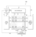
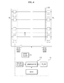
- FIG. 1 is a block diagram of a display device according to an embodiment of the present invention.
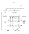
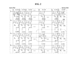
- FIG. 2 is a circuit diagram of a pixel array of a display device according to an embodiment of the present invention.
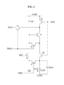
- FIG. 3 is an equivalent circuit diagram schematically illustrating one active pixel of a display device according to an embodiment of the present invention.
- FIG. 4 is a block diagram of a control unit of a display device according to an embodiment of the present invention.
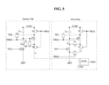
- FIG. 5 is an equivalent circuit diagram of one active pixel driving circuit and one dummy pixel driving circuit connected to each other in a display device according to an embodiment of the present invention.
- FIG. 6 is an equivalent circuit diagram of one active pixel driving circuit and one dummy pixel driving circuit in a display device according to another embodiment of the present invention.
- FIG. 7 is an equivalent circuit diagram of one active pixel driving circuit and one dummy pixel driving circuit in a display device according to still another embodiment of the present invention.
- FIG. 8 is an equivalent circuit diagram of one active pixel driving circuit and one dummy pixel driving circuit in a display device according to still another embodiment of the present invention.
- FIG. 9 is a timing diagram illustrating a level change of a signal that is applied to a display device according to still another embodiment of the present invention.
- FIGS. 10 through 13 are equivalent circuit diagrams of one active pixel driving circuit and one dummy pixel driving circuit in a display device according to still another embodiment of the present invention.
- FIG. 14 is an equivalent circuit diagram of one active pixel driving circuit and one dummy pixel driving circuit in a display device according to still another embodiment of the present invention.
- FIG. 15 is a timing diagram illustrating a level change of a signal that is applied to a display device according to still another embodiment of the present invention.
- an element or layer When an element or layer is referred to as being “on,” “connected to,” or “coupled to” another element or layer, it may be directly on, connected to, or coupled to the other element or layer or intervening elements or layers may be present. When, however, an element or layer is referred to as being “directly on,” “directly connected to,” or “directly coupled to” another element or layer, there are no intervening elements or layers present.
- “at least one of X, Y, and Z” and “at least one selected from the group consisting of X, Y, and Z” may be construed as X only, Y only, Z only, or any combination of two or more of X, Y, and Z, such as, for instance, XYZ, XYY, YZ, and ZZ.
- Like numbers refer to like elements throughout.
- the term “and/or” includes any and all combinations of one or more of the associated listed items.
- first, second, etc. may be used herein to describe various elements, components, regions, layers, and/or sections, these elements, components, regions, layers, and/or sections should not be limited by these terms. These terms are used to distinguish one element, component, region, layer, and/or section from another element, component, region, layer, and/or section. Thus, a first element, component, region, layer, and/or section discussed below could be termed a second element, component, region, layer, and/or section without departing from the teachings of the present disclosure.
- Spatially relative terms such as “beneath,” “below,” “lower,” “above,” “upper,” and the like, may be used herein for descriptive purposes, and, thereby, to describe one element or feature's relationship to another element(s) or feature(s) as illustrated in the drawings.
- Spatially relative terms are intended to encompass different orientations of an apparatus in use, operation, and/or manufacture in addition to the orientation depicted in the drawings. For example, if the apparatus in the drawings is turned over, elements described as “below” or “beneath” other elements or features would then be oriented “above” the other elements or features.
- the exemplary term “below” can encompass both an orientation of above and below.
- the apparatus may be otherwise oriented (e.g., rotated 90 degrees or at other orientations), and, as such, the spatially relative descriptors used herein interpreted accordingly.
- FIG. 1 is a block diagram of a display device according to an embodiment of the present invention.
- an organic light emitting display 1000 includes a display panel 100 .
- the display panel 100 may include a plurality of pixels PX and wirings for transferring signals to the plurality of pixels PX.
- the plurality of pixels PX may be arranged in the form of a matrix. Each of the plurality of pixels PX may emit light with one color of red, green, and blue.
- Light emission of the plurality of pixels PX may be controlled by first to n-th scan signals S 1 to Sn, first to m-th data signals D 1 to Dm, and first to n-th light emission signals Em 1 to Emn, which are provided from outside of the display panel 100 .
- the first to n-th scan signals S 1 to Sn may control whether the plurality of pixels PX receive the first to m-th data signals D 1 to Dm.
- the first to m-th data signals D 1 to Dm may include information on luminance of light emitted from the plurality of pixels PX.
- the first to m-th light emission signals Em 1 to Emn may control whether the plurality of pixels PX emit light.
- the wirings may include wirings for transferring the first to n-th scan signals S 1 to Sn, the first to m-th data signals D 1 to Dm, the first to m-th light emission signals Em 1 to Emn, and an initialization voltage VINIT.
- the wirings for transferring the first to n-th scan signals S 1 to Sn and the first to m-th light emission signals Em 1 to Emn may be arranged to extend in a row direction of the plurality of pixels PX.
- the wirings for transferring the first to m-th data signals D 1 to Dm may be arranged to extend in a column direction of the plurality of pixels PX.
- the wirings for transferring the initialization voltage VINIT may be formed in a zigzag form (not shown).
- the organic light emitting display 1000 may further include a driving unit and a voltage generation unit 15 .
- the driving unit may include a control unit 11 , a data driving unit 12 , a scan driving unit 13 , and a light emission driving unit 14 .
- the control unit 11 may receive video data from an outside, and may generate a scan driving unit control signal SCS that can control the scan driving unit 13 , a date driving unit control signal DCS that can control the data driving unit 12 , and a light emission driving unit control signal ECS that can control the light emission driving unit 14 in response to the received video data.
- the driving unit may further include a comparison unit(not shown) determining whether each pixel driving circuit has inferiority, and a synchronization unit (not shown) synchronizing an output signal of a dummy driving circuit with a data signal that is provided to the pixel driving circuit.
- the data driving unit 12 may receive the data driving unit control signal DCS, and may generate the first to m-th data signals D 1 to Dm in response to the received data driving unit control signal DCS.
- the scan driving unit 13 may receive the scan driving unit control signal SCS, and may generate the first to n-th scan signals S 1 to Sn in response to the received scan driving unit control signal SCS.
- the light emission driving unit 14 may receive the light emission driving unit control signal ECS, and may generate the first to n-th light emission signals Em 1 to Emn in response to the received light emission driving unit control signal ECS.
- the voltage generation unit 15 may generate the initialization voltage VINIT, a first power voltage ELVDD, and a second power voltage ELVSS to provide such voltages to the display panel 100 .
- the initialization voltage VINIT, the first power voltage ELVDD, and the second power voltage ELVSS may vary, and the control unit 11 may control the voltage generation unit 15 to change the initialization voltage VINIT, the first power voltage ELVDD, and the second power voltage ELVSS.
- FIG. 2 is a circuit diagram of a pixel array of a display device according to an embodiment of the present invention.
- Each circuit in the pixels P 11 to Pnm and the dummy cells DC 1 to DCn disclosed in FIG. 2 is an exemplary embodiment for showing the pixel array and the each circuit will be described in detail with reference to FIGS. 3 through 14 .
- a substrate includes a pixel array area (active area) and a dummy area adjacent to the pixel array area (active area).
- Pixels P 11 to Pnm may be arranged in the pixel array area (active area), and dummy cells DC 1 to DCn may be arranged in the dummy area.
- Scan lines S 1 to Sn may be arranged in one direction in the pixel array area (active area) and the dummy area.
- Data lines D 1 to Dm may be arranged to cross the scan lines S 1 to Sn in the pixel array area (active area).
- the pixels P 11 to Pnm are defined by the scan lines S 1 to Sn and the data lines D 1 to Dm, which extend to cross each other.
- a dummy data line Dd may be arranged to cross the scan lines S 1 to Sn in the dummy area.
- the dummy cells DC 1 to DCn may be defined by crossing of the scan lines S 1 to Sn and the dummy data line Dd.
- Each of the pixels P 11 to Pnm may include a pixel electrode and a pixel driving circuit (active pixel) electrically connected to the pixel electrode.
- the pixel driving circuit (active pixel) as disclosed in P 11 may include a switching transistor M 1 , a capacitor Cst, and a driving transistor M 2 .
- the switching transistor M 1 may include a gate electrode connected to the scan line S 1 and a source electrode connected to the data line D 1 and may switch a data signal applied to the data line D 1 according to a scan signal applied to the scan line S 1 .
- the capacitor Cst may be connected between a drain electrode of the switching transistor M 1 and the line to which a first power voltage ELVDD is applied to maintain the data signal for a predetermined period.
- the driving transistor M 2 may include a gate electrode connected to the capacitor Cst, a source electrode connected to the line to which the first power voltage ELVDD is applied, and a drain electrode connected to a light emitting element EL, and may supply current that is in proportion to the size of the data signal to the light emitting element EL, specifically, a pixel electrode of the light emitting element EL.
- the light emitting element EL may emit light corresponding to the current supplied thereto.
- the pixel driving circuit active pixel
- FIG. 3 The pixel driving circuit (active pixel) according to an embodiment of the present invention will be described in detail with reference to FIG. 3 .
- each of the dummy cells DC 1 to DCn may include a dummy driving circuit (dummy pixel) for applying an electrical signal to the pixel electrode.
- the dummy driving circuit (dummy pixel) may be connected to the scan lines S 1 to Sn, the dummy data line Dd, and the terminal of the first power voltage ELVDD.
- the dummy driving circuit (dummy pixel) as disclosed in DC 1 may include a switching transistor M 1 , a capacitor Cst, and a driving transistor M 2 .
- the switching transistor M 1 includes a gate electrode connected to the scan line S 1 and a source electrode connected to the dummy data line Dd, and may switch a data signal applied to the dummy data line Dd according to a scan signal applied to the scan line S 1 .
- the capacitor Cst may be connected between the drain electrode of the switching transistor M 1 and the terminal of the first power voltage ELVDD to maintain the data signal for a predetermined period.
- the driving transistor M 2 may include a gate electrode connected to the capacitor Cst and a source electrode connected to the line of the first power voltage ELVDD.
- the dummy lines DL 1 to DLn that are electrically connected to the dummy driving circuit (dummy pixel), specifically, the drain electrode of the driving transistor M 2 , may be arranged in the dummy area.
- the dummy lines DL 1 to DLn may extend toward the pixel array area (active area) and may be arranged on lower portions of the pixel electrodes.
- the pixel electrodes may overlap the dummy lines DL 1 to DLn.
- inferiority may occur in the pixel driving circuit (active pixel) that is positioned on a part of the pixels.
- the light emitting element EL that is connected to the pixel driving circuit (active pixel) in which the inferiority has occurred may not emit light even in an on-state or may emit light even in an off-state to cause dark spot or bright spot inferiority.
- wirings between the pixel driving circuit (active pixel) of the pixel in which the inferiority has occurred and the light emitting element EL may be disconnected.
- the wirings between the pixel driving circuit (active pixel) of the Pab pixel, specifically, the driving transistor M 2 of the Pab pixel, and the light emitting element EL may be disconnected.
- the wirings between the pixel driving circuit (active pixel) and the light emitting element EL may not be disconnected, for example, in the case where an electrical signal is not applied to the light emitting element EL due to the defect that is generated in the pixel driving circuit (active pixel).
- the dummy lines DLa arranged in the lower portion of the pixel electrode of the Pab pixel may be electrically connected.
- the electrical connection of the dummy lines DLa arranged in the lower portion of the pixel electrode of the Pab pixel may be performed by using a laser repairing method.
- the pixel electrode of the Pab pixels may be electrically connected to the dummy driving circuit (dummy pixel) that is positioned in the dummy cell DCa.
- the Pab pixel is driven by selecting the Sa scan line and applying a data voltage to the data line Dd.
- the Pab pixel may not cause the bright spot or dark spot inferiority.
- FIG. 3 is an equivalent circuit diagram schematically illustrating one active pixel of a display device according to an embodiment of the present invention.
- one active pixel of an organic light emitting display includes a plurality of pixel transistors T 1 , T 2 , T 3 , T 4 , T 5 , T 6 , and T 7 to which a plurality of signals may be applied, a storage capacitor Cst, and an organic light emitting diode OLED.
- the pixel transistors may include a first pixel transistor T 1 , a second pixel transistor T 2 , a third pixel transistor T 3 , a fourth pixel transistor T 4 , a fifth pixel transistor T 5 , a sixth pixel transistor T 6 , and a seventh pixel transistor T 7 .
- the plurality of signals may include a scan signal GW[n], a previous scan signal GI[n], a light emission control signal En[n], a data signal D[n], a first power voltage ELVDD, a second power voltage ELVSS, an initialization voltage Vint, and a black voltage signal GB[n].
- the gate electrode of the first pixel transistor T 1 may be connected to one terminal of the storage capacitor Cst, and the source electrode of the first pixel transistor T 1 may be connected to the first power voltage ELVDD through the fifth pixel transistor T 5 .
- the drain electrode of the first pixel transistor T 1 may be electrically connected to the anode of the organic light emitting diode OLED through the sixth pixel transistor T 6 .
- the first pixel transistor T 1 may receive the data signal D[n] according to the switching operation of the second pixel transistor T 2 , and may supply driving current IDLED to the organic light emitting diode OLED.
- the gate electrode of the second pixel transistor T 2 may receive the scan signal GW[n], and the source electrode of the second pixel transistor T 2 may receive the data signal D[n].
- the drain electrode of the second pixel transistor T 2 may be connected to the source electrode of the first pixel transistor T 1 and may receive the first power voltage ELVDD through the fifth pixel transistor T 5 .
- the second pixel transistor T 2 may be turned on according to the scan signal GW[n] to perform switching operation for transferring the data signal D[n] to the source electrode of the first pixel transistor T 1 .
- the gate electrode of the third pixel transistor T 3 may receive the scan signal GW[n], and the source electrode of the third pixel transistor T 3 may be connected to the drain electrode of the first pixel transistor T 1 and may also be connected to the anode of the organic light emitting diode OLED through the sixth pixel transistor T 6 .
- the drain electrode of the third pixel transistor T 3 may be connected to one terminal of the storage capacitor Cst, the drain electrode of the fourth pixel transistor T 4 , and the gate electrode of the first pixel transistor T 1 .
- the third pixel transistor T 3 may be turned on according to the scan signal GW[n], which makes the gate electrode and the drain electrode of the first pixel transistor T 1 connected to each other, and thus the first pixel transistor T 1 is diode-connected.
- the gate electrode of the fourth pixel transistor T 4 receives the previous scan signal GI[n], and the source electrode of the fourth pixel transistor T 4 receives the initialization voltage Vint.
- the drain electrode of the fourth pixel transistor T 4 is connected to one terminal of the storage capacitor Cst, the drain electrode of the third pixel transistor T 3 , and the gate electrode of the first pixel transistor T 1 .
- the fourth pixel transistor T 4 may be turned on according to the previous scan signal GI[n] to transfer the initialization voltage Vint to the gate electrode of the first pixel transistor T 1 , and thus the voltage of the gate electrode of the first pixel transistor T 1 may be initialized.
- the gate electrode of the fifth pixel transistor T 5 may receive the light emission control signal En[n], and the source electrode of the fifth pixel transistor T 5 may receive the first power voltage ELVDD.
- the drain electrode of the fifth pixel transistor T 5 may be connected to the source electrode of the first pixel transistor T 1 and the drain electrode of the second pixel transistor T 2 .
- the gate electrode of the sixth pixel transistor T 6 may receive the light emission control signal En[n], and the source electrode of the sixth pixel transistor T 6 may be connected to the drain electrode of the first pixel transistor T 1 and the source electrode of the third pixel transistor T 3 .
- the drain electrode of the sixth pixel transistor T 6 may be electrically connected to the anode of the organic light emitting diode OLED and the drain electrode of the seventh pixel transistor T 7 .
- the fifth pixel transistor T 5 and the sixth pixel transistor T 6 may be simultaneously turned on according to the light emission control signal En[n], and thus the first power voltage ELVDD is transferred to the organic light emitting diode OLED to make the driving current I OLED flow to the organic light emitting diode OLED.
- the gate electrode of the seventh pixel transistor T 7 may receive the black voltage signal GB[n], and the source electrode of the seventh pixel transistor T 7 may receive the initialization voltage Vint.
- the drain electrode of the seventh pixel transistor T 7 may be connected to the anode of the organic light emitting diode OLED and the drain electrode of the sixth pixel transistor T 6 .
- the seventh pixel transistor T 7 may be turned on according to the black voltage signal GB[n], and thus the initialization voltage Vint may be transferred to the anode of the organic light emitting diode OLED to apply the black voltage thereto.
- the other terminal of the storage capacitor Cst may be connected to the first power voltage ELVDD, and the cathode of the organic light emitting diode OLED may be connected to the second power voltage ELVSS. Accordingly, the organic light emitting diode OLED may receive the driving current IDLED from the first pixel transistor T 1 and may emit light to display an image.
- the pixel includes seven transistors and an organic light emitting diode OLED, but is not limited thereto.
- the pixel included in the organic light emitting display may include a plurality of transistors and organic light emitting diodes OLED.
- FIG. 4 is a block diagram of a control unit of a display device according to an embodiment of the present invention.
- a dummy pixel unit may be disposed on both side of the display panel 100 .
- the dummy pixel unit may be connected to the control unit 11 through repair wirings RL.
- the dummy pixel unit may include a plurality of dummy driving circuits connected to the scan lines.
- FIG. 4 illustrates that the dummy pixel unit is formed at both terminals of the scan lines, but is not limited thereto.
- the dummy pixel unit may be formed at both terminals of the data lines, or may be formed at both terminals of the data lines and the scan lines.
- the control unit 11 may apply DATA to each of the pixel driving circuits (active pixels), and may receive PR_ON that shows whether the pixel driving circuits (active pixels) have inferiority which may be sensed by a sensing element (not illustrated).
- the sensing element receives PR_COL and PR_ROW that shows the positon of the pixel driving circuits (active pixels) having inferiority.
- a comparator 115 of the control unit 11 may determine positions of the individual pixel driving circuits (active pixels) in which the inferiority has occurred and the size of data to be applied to the individual pixel driving circuits (active pixels) and may apply corresponding signals to the repair wirings RL through collection of the PR_ON, the PR_COL and the PR_ROW.
- the signals that the comparator 115 provides to the repair wirings RL may include a synchronization signal Vsync so that the signals and the data signals from data lines(not shown) can be synchronized with each other to be simultaneously output.
- the signals that the comparator 115 provides to the repair wirings RL may be provided through a repair buffer (DR-IC repair buffer).
- the method for sensing the pixel driving circuits in which the inferiority has occurred and the method for applying data to the pixel driving circuit (active pixel) in which the inferiority has occurred are not limited to those as described above.
- FIG. 5 is an equivalent circuit diagram of one active pixel driving circuit and one dummy driving circuit connected to each other in a display device according to an embodiment of the present invention.
- the dummy driving circuit (dummy pixel) and the pixel driving circuit (active pixel) may be formed to have the same structure.
- the inferiority may occur in the pixel driving circuit (active pixel) that is positioned in a part of the pixels.
- the wirings between the pixel driving circuit (active pixel) of the pixel in which the inferiority has occurred and the organic light emitting diode OLED may be disconnected.
- the drain electrodes of the sixth and seventh transistors T 6 and T 7 of the pixel driving circuit (active pixel) may be open from the anode of the organic light emitting diode OLED at node A (a first pixel node), and the drain electrode of the sixth dummy transistor Td 6 of the dummy driving circuit (dummy pixel) may be connected to the anode of the organic light emitting diode OLED at node A′ (a first dummy node).
- the wirings between the pixel driving circuit (active pixel) and the light emitting element EL may not be disconnected in the case where any electrical signal is not applied to the organic light emitting diode OLED due to the defect that is generated in the pixel driving circuit (active pixel).
- the dummy driving circuit (dummy pixel) and the pixel driving circuit (active pixel) may be connected by the repair wirings, and the repair wirings may be connected to the dummy pixel unit crossing the display panel 100 that may be formed at both ends of the display panel 100 .
- the repair wirings may be composed of a conductive material, but the level of a voltage that is applied to each pixel driving circuit (active pixel) may be decreased due to the resistance of the repair wirings.
- the dummy driving circuits of the dummy pixels formed at the both ends of the display panel 100 may be disposed in a first direction (row) and be electrically connected through the repair wirings at the first dummy node (node A′) of the dummy driving circuit.
- the dummy driving circuit may include a seventh dummy transistor Td 7 (A dummy transistor).
- the control electrode(gate) of the seventh dummy transistor Td 7 may be connected to the control electrode of the first dummy transistor Td 1 as a dummy driving transistor, and the output electrode (drain) of the seventh dummy transistor Td 7 may be connected to the output electrode of the first dummy transistor Td 1 .
- the input electrode (source) of the seventh dummy transistor Td 7 may be connected to the output electrode of the third dummy transistor Td 3 (B dummy transistor).
- the third dummy transistor Td 3 is turned on in response to the scan signal GW[n] and connects the output electrode and the control electrode of the first dummy transistor Td 1 through the seventh dummy transistor Td 7 in turn-on state to each other, and then the first dummy transistor Td 1 is diode-connected. Further, the third dummy transistor Td 3 connects the control electrode and the output electrode of the seventh dummy transistor Td 7 through the first dummy transistor in turn-on state to each other, and thus the seventh dummy transistor Td 7 is diode-connected. Consequently, the first dummy transistor Td 1 and the seventh dummy transistor Td 7 are diode-connected to be forward-biased by the third dummy transistor in turn-on state.
- a compensation voltage decreased from the data signal D[n] by a threshold voltage Vth of the first dummy transistor Td 1 is applied to the gate electrode of the first dummy transistor Td 1 .
- the first power voltage ELVDD and the compensation voltage are applied to both terminals of the storage capacitor Cst, and electric charge generated from a voltage difference between the both terminals of the storage capacitor Cst is stored in the storage capacitor Cst. Accordingly, the level of the light emission signal EM[n] is changed from high level to low level, and thus during the light emission period, the fifth and sixth dummy transistors Td 5 and Td 6 are turned on by the low-level light emission control signal EM[n].
- a driving current that corresponds to the voltage difference between the control electrode of the first dummy transistor Td 1 and the first power voltage ELVDD is generated, and the driving current through the sixth dummy transistor Td 6 is transferred to the pixel driving circuit (active pixel) through node A′.
- the voltage Vgs between the control electrode and the output electrode of the first dummy transistor Td 1 is maintained constant by the storage capacitor Cst, and the driving current is in proportion to a square of a value that is obtained by subtracting the threshold voltage Vth from the voltage Vgs between the control electrode and the output electrode of the first dummy transistor Td 1 .
- the seventh dummy transistor Td 7 is connected to the first dummy transistor Td 1 , and it is effective that the channel length of the first dummy transistor Td 1 during the compensation period is lengthened twice the channel length of the first pixel transistor T 1 .
- the channel length of the first dummy transistor Td 1 during the compensation period is lengthened twice the channel length of the first dummy transistor Td 1 during the light emission period through combination of the first dummy transistor Td 1 and the seventh dummy transistor Td 7 , and thus compensation becomes possible with a lower voltage of the control electrode of the first dummy transistor Td 1 . Accordingly, it is possible to generate larger current than the current of the pixel driving circuit (active pixel) with respect to the same data voltage, and thus the increase of the resistance due to the repair wirings can be offset.
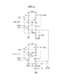
- FIG. 6 is an equivalent circuit diagram of one pixel driving circuit and one dummy driving circuit in a display device according to another embodiment of the present invention.
- Parasitic capacitance may be formed between node G of the pixel driving circuit (active pixel) and a terminal to which the scan signal GW[n] is applied and between the node G of the pixel driving circuit (active pixel) and the node A. Further, parasitic capacitance may also be formed between node G′ (a second dummy node) of the dummy driving circuit (dummy pixel) and the terminal to which the scan signal GW[n] is applied and between the node G′ of the dummy driving circuit (dummy pixel) and node A′.
- the first thin film transistor T 1 of the pixel driving circuit and the first dummy transistor Td 1 of the dummy driving circuit may be unable to provide an accurate driving current that corresponds to the data signal to the organic light emitting diode OLED.
- the gate electrodes of the fourth pixel transistor T 4 and the seventh pixel transistor T 7 of the pixel driving circuit may be electrically connected to each other, and the fourth pixel transistor T 4 and the seventh pixel transistor T 7 may be driven by the signal GI[n].
- the pixel driving circuit (active pixel) and the dummy driving circuit (dummy pixel) may be connected to each other by the repair wirings, and the repair wirings may be formed to overlap the individual pixel driving circuit (active pixel) and to extend in a row direction (a first direction). If inferiority occurs in the pixel driving circuit (active pixel), the driving current that corresponds to the data signal may be applied to the organic light emitting diode OLED of the pixel driving circuit (active pixel) that is connected to the dummy driving circuit (dummy pixel) by the repair wirings.
- repair wirings are formed to overlap the pixel electrode of the individual pixel, very high anode parasitic capacitance may be formed in the repair wirings.
- the pixel electrode and the repair wirings may be coupled to each other at a specific voltage, and a boost voltage may be formed at the anode of the organic light emitting diode OLED of the pixel driving circuit (active pixel).
- the boost voltage may increase the level of the voltage that is applied to the node A of the pixel driving circuit (active pixel), and even if a black signal is applied through this, the voltage of the anode of the organic light emitting diode OLED of the pixel driving circuit (active pixel) becomes higher than the cathode voltage by the boost voltage to cause somewhat light to be emitted.
- an initialization line (not illustrated) may be formed in parallel to the repair wirings, and fringe capacitance may be generated due to the initialization line (not illustrated) and the repair wirings.
- the fringe capacitance may exert an influence on the individual pixel driving circuit (active pixel) according to the voltage that is applied to the gate electrode. That is, the parasitic capacitance may be formed by the initialization line (not illustrated) and the repair wirings.
- the dummy driving circuit (dummy pixel) disclosed in FIG. 6 may further include a first pumping transistor Tp 1 connected to the node A′ of the dummy driving circuit (dummy pixel), a second pumping transistor Tp 2 , and a pumping capacitor Cp.
- the control electrode of the first pumping transistor Tp 1 may receive the scan signal GW[n], and the output electrode thereof may be connected to the node A′ of the dummy driving circuit (dummy pixel).
- the input electrode of the first pumping transistor Tp 1 may be connected to the output electrode of the second pumping transistor Tp 2 at a pumping node Pnode (a third dummy node).
- the control electrode of the second pumping transistor Tp 2 may receive the initialization signal GI[n], the output electrode thereof may be connected to the input electrode of the first pumping transistor Tp 1 at the pumping node Pnode, and the input electrode thereof may receive the initialization voltage VINIT applied thereto.
- the pumping capacitor Cp may connect the pumping node Pnode and the terminal to which the first power voltage ELVDD is applied to each other.
- the first pumping transistor Tp 1 may connect the node A′ of the dummy driving circuit (dummy pixel) and the pumping capacitor Cp to each other in response to the scan signal GW[n] to reduce the amount of charge that is charged by the parasitic capacitance that may be generated in the repair wirings. That is, the parasitic capacitor that may be generated in the repair wirings and the pumping capacitor Cp may be connected in parallel and they may share the electric charge that may be generated in the repair wirings which may be charged only in the parasitic capacitor.
- the organic light emitting diode OLED when the data signal having low grayscale is applied by the first and second pumping transistors Tp 1 and Tp 2 and the pumping capacitor Cp, the organic light emitting diode OLED can be prevented from emitting light somewhat brightly through addition of the pumping capacitor Cp, the organic light emitting diode OLED can be prevented from emitting light somewhat darkly when the data signal having high grayscale is applied.
- the second pumping transistor Tp 2 may apply the initialization voltage VINIT to the pumping node Pnode in response to the initialization signal GI[n].
- One terminal of the pumping capacitor Cp may be connected to the pumping node Pnode, and the other terminal thereof may be connected to the terminal to which the first power voltage ELVDD is applied.
- the other terminal of the pumping capacitor Cp may not be limited to being connected to the terminal to which the first power voltage ELVDD is applied, but may be connected to a terminal to which a constant voltage can be applied.
- the second pumping transistor Tp 2 is not limited to being formed, but may be omitted if needed.
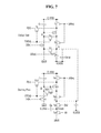
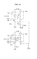
- FIG. 7 is an equivalent circuit diagram of one pixel driving circuit and one dummy driving circuit in a display device according to still another embodiment of the present invention.
- FIG. 7 illustrates a circuit having a similar structure to the structure of the circuit illustrated in FIG. 6 , explanation of the duplicate constituent elements will be omitted.
- the control terminals of the fourth pixel transistor T 4 and the seventh pixel transistor T 7 of the pixel driving circuit may be electrically separated from each other, and the fourth pixel transistor T 4 and the seventh pixel transistor T 7 may be turned on with different timings by the initialization signal GI[n] and the black voltage signal GB[n], respectively.
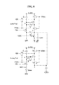
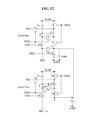
- FIG. 8 is an equivalent circuit diagram of one pixel driving circuit and one dummy driving circuit in a display device according to still another embodiment of the present invention.
- the control terminals of the fourth pixel transistor T 4 and the seventh pixel transistor T 7 of the pixel driving circuit may be electrically separated from each other, and the fourth pixel transistor T 4 and the seventh pixel transistor T 7 may be driven by the initialization signal GI[n] and the black voltage signal GB[n], respectively.
- the pixel driving circuit (active pixel) and the dummy driving circuit (dummy pixel) may be connected to each other by the repair wirings.
- data may be applied to the organic light emitting diode OLED of the pixel driving circuit (active pixel) that is connected to the dummy driving circuit (dummy pixel) by the repair wirings.
- the dummy driving circuit (dummy pixel) and the individual pixel driving circuit (active pixel) may be connected to each other by the repair wirings, and the repair wirings may be formed to overlap the individual pixel driving circuit (active pixel) and to extend in a row direction. Since the repair wirings are formed to overlap the pixel electrode of the individual pixel, very high anode parasitic capacitance may be formed in the repair wirings.
- the dummy driving circuit (dummy pixel) disclosed in FIG. 8 may further include a boost diode Diode that is connected to the fourth dummy transistor Td 4 (C dummy transistor) of the dummy driving circuit (dummy pixel).
- the anode terminal of the boost diode Diode may be connected to the input terminal of the fourth dummy transistor TD 4 , and the cathode terminal thereof may be connected to the terminal to which the initialization voltage VINIT is applied.
- the level of the voltage Vgs between the control electrode and the output electrode of the first dummy transistor Td 1 can be reduced.
- the current that flows to the node A′ of the dummy driving circuit (dummy pixel) can be reduced, and thus the amount of electric charge that is charged in the parasitic capacitor that may be generated in the repair wirings can also be reduced.
- the boost voltage VBST is also reduced, and even if the black data and data having low grayscale are applied, the phenomenon that the organic light emitting diode OLED emits light somewhat brightly can be reduced.
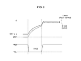
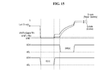
- FIG. 9 is a timing diagram illustrating a level change of a signal that is applied to a display device according to still another embodiment of the present invention.
- the voltage of a node G′ of the dummy driving circuit (dummy pixel) is increased on the basis of the initialization voltage VINIT+a that is increased by the boost diode Diode ( FIG. 8 ).
- the node G′ of the dummy driving circuit (dummy pixel) and the node G of the pixel driving circuit (active pixel) start to be increased at different voltage levels, and thus the voltage of the node G′ of the dummy driving circuit (dummy pixel) may be maintained higher than the voltage of the node G of the pixel driving circuit (active pixel).
- the voltage of the node G′ of the dummy driving circuit (dummy pixel) is maintained higher than the voltage of the node G of the pixel driving circuit (active pixel), the voltage Vgs between the control electrode and the output electrode of the first dummy transistor Td 1 of the dummy driving circuit (dummy pixel) is lowered, and the driving current that flows to the first dummy transistor Td 1 is lowered. Accordingly, even if the black data and the low-grayscale data signal are applied, the phenomenon that the organic light emitting diode OLED emits light somewhat brightly can be reduced.
- the voltage is somewhat increased by the self capacitance of the third dummy transistor Td 3 , but it may be assumed that constant voltage can be maintained to some extent although it is mainly changed according to the threshold voltage of the third dummy transistor Td 3 and a design layout of the circuit.
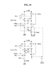
- FIGS. 10 through 13 are equivalent circuit diagrams of one pixel driving circuit and one dummy driving circuit in a display device according to still another embodiment of the present invention.
- FIGS. 10 through 13 illustrate circuits having similar structure to the structure of the circuit of FIG. 8 , explanation of the duplicate constituent elements will be omitted.
- the control electrodes of the fourth pixel transistor T 4 and the seventh pixel transistor T 7 of the pixel driving circuit may be electrically connected to each other, and the fourth pixel transistor T 4 and the seventh pixel transistor T 7 may be driven by the signal GI[n].
- the voltage level of the repair wirings may be increased at a rising edge of the initialization signal GI[n].
- a boost transistor Tu may be included instead of the boost diode Diode of FIG. 8 .
- the control electrode of the boost transistor Tu may be connected to the input electrode of the boost transistor Tu to form a diode connection. Due to the diode connection, the boost transistor Tu may serve as a diode, and may apply the initialization voltage VINIT+a, which is increased by the threshold voltage Vth of the boost transistor Tu, to the fourth dummy transistor Td 4 .
- the level of the voltage Vgs of the first dummy transistor Td 1 can be reduced. Further, as the level of the voltage Vgs between the control electrode and the output electrode of the first dummy transistor Td 1 is lowered, the current that flows to the node A′ of the dummy driving circuit (dummy pixel) can be reduced, and thus the amount of electric charge that is charged in the parasitic capacitor that may be generated in the repair wirings can also be reduced. As the amount of the electric charge that is charged in the parasitic capacitor that may be generated in the repair wirings is reduced, the boost voltage level is also reduced, and even if the black data and low-grayscale data are applied, the phenomenon that the organic light emitting diode OLED emits light somewhat brightly can be reduced.
- FIG. 11 illustrates a structure in which the control electrodes of the fourth pixel transistor T 4 and the seventh pixel transistor T 7 of the pixel driving circuit (active pixel) are electrically separated from each other, but are not limited thereto.
- the structure may be modified to a structure in which the control electrodes of the fourth pixel transistor T 4 and the seventh pixel transistor T 7 of the pixel driving circuit (active pixel) are connected to each other.
- the boosted voltage may be directly applied to the fourth dummy transistor instead of the boost diode Diode of FIG. 8 .
- the level of the voltage Vgs between the control electrode and the output electrode of the first dummy transistor Td 1 can be reduced.
- the current that flows to the node A′ of the dummy driving circuit (dummy pixel) can be reduced, and thus the amount of electric charge that is charged in the parasitic capacitor that may be generated in the repair wirings can also be reduced.
- the boost voltage can be reduced, and thus even if the black data and the low-grayscale data are applied, the phenomenon that the organic light emitting diode OLED emits light somewhat brightly.
- the boost diode Diode is not formed for each line of the individual pixel driving circuit (active pixel), but may be formed on lines of a plurality of pixel driving circuits (active pixels).
- the boost diode Diode is a constituent element that is added to apply the boosted voltage that is higher than the initialization voltage VINIT to the fourth dummy transistors Td 4 , and even if the fourth dummy transistors Td 4 of the plurality of pixel driving circuits (active pixels) are connected to the anode terminal of the boost diode Diode, the driving current of the first dummy transistor Td 1 of each pixel driving circuit (active pixel) can be reduced.
- FIG. 13 illustrates the boost diode Diode that is connected to the plurality of pixel driving circuits (active pixels), but is not limited thereto.
- a structure, which connects the source terminal of the boost transistor Tu to the drain electrodes of the plurality of fourth dummy transistors Td 4 or which applies the boosted voltage to the drain electrodes of the plurality of fourth dummy transistors Td 4 may be included.
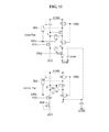
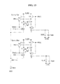
- FIG. 14 is an equivalent circuit diagram of one pixel driving circuit and one dummy driving circuit in a display device according to still another embodiment of the present invention
- FIG. 15 is a timing diagram illustrating a level change of a signal that is applied to a display device according to still another embodiment of the present invention.
- FIG. 14 illustrates a circuit having a similar structure to the structure of the circuit illustrated in FIG. 10 , explanation of the duplicate constituent elements will be omitted.
- the control electrodes of the fourth pixel transistor T 4 and the seventh pixel transistor T 7 of the pixel driving circuit may be electrically separated from each other, and the fourth pixel transistor T 4 and the seventh pixel transistor T 7 may be driven by the initialization signal GI[n] and the black voltage signal GB[n], respectively.
- the dummy driving circuit (dummy pixel) may further include a boost capacitor Cbst that connects the terminal to which the initialization signal GI[n] is applied to the dummy driving circuit (dummy pixel).
- the boost capacitor Cbst is connected to the node G′ of the dummy driving circuit (dummy pixel), and when the high-level initialization signal GI[n] is applied, it boosts the voltage of the node G′.
- the level of the voltage Vgs between the control electrode and the output electrode of the first dummy transistor Td 1 can be reduced.
- the current that flows to the anode of the dummy driving circuit (dummy pixel) can be reduced, and thus the amount of electric charge that is charged in the parasitic capacitor that may be generated in the repair wirings can also be reduced.
- the boost voltage is also reduced, and even if the black data and the data having low grayscale are applied, the phenomenon that the organic light emitting diode OLED emits light somewhat brightly can be reduced.
- FIG. 14 illustrates the structure in which the control electrodes of the fourth pixel transistor T 4 and the seventh pixel transistor T 7 of the pixel driving circuit (active pixel) are electrically separated from each other, but is not limited thereto.
- a structure, in which the control electrodes of the fourth pixel transistor T 4 and the seventh pixel transistor T 7 are electrically connected, may be included.
- the initialization signal GI[n] is increased from low level to high level, and a voltage that is higher than the voltage that is increased by the initialization voltage VINIT and the parasitic capacitance of the fourth dummy transistor Td 4 is charged in the boost capacitor Cbst that is connected to the terminal to which the initialization signal GI[n] is applied.
- the voltage of the node G′ of the dummy driving circuit (dummy pixel) is increased on the basis of the initialization voltage that is increased by the boost capacitor Cbst and the parasitic capacitance of the transistor Td 4 .
- the dummy driving circuit (dummy pixel) and the pixel driving circuit (active pixel) start to be increased at different voltage levels, and thus the voltage of the node G′ of the dummy driving circuit (dummy pixel) may be maintained higher than the voltage of the node G of the pixel driving circuit (active pixel).
- the voltage of the node G′ of the dummy driving circuit (dummy pixel) is maintained to be higher than the voltage of the G node G of the pixel driving circuit (active pixel), the voltage Vgs between the control electrode and the output electrode of the first dummy transistor Td 1 of the dummy driving circuit (dummy pixel) is lowered, and the driving current that flows to the first dummy transistor Td 1 is lowered. Accordingly, even if the black data and the low-grayscale data signal are applied, the phenomenon that the organic light emitting diode OLED emits light somewhat brightly can be reduced.
- the voltage is somewhat increased by the self capacitance of the third dummy transistor Td 3 , but it may be assumed that constant voltage can be maintained to some extent although it is mainly changed according to the threshold voltage of the third dummy transistor Td 3 and the design layout of the circuit.
Landscapes
- Engineering & Computer Science (AREA)
- Physics & Mathematics (AREA)
- Computer Hardware Design (AREA)
- General Physics & Mathematics (AREA)
- Theoretical Computer Science (AREA)
- Control Of El Displays (AREA)
- Electroluminescent Light Sources (AREA)
- Control Of Indicators Other Than Cathode Ray Tubes (AREA)
Abstract
Description
- This application claims priority from and the benefit of Korean Patent Application No. 10-2014-0173960, filed on Dec. 5, 2014, which is hereby incorporated by reference for all purposes as if fully set forth herein.
- 1. Field
- Exemplary embodiments relate to a display device, and more particularly to a repairable display device.
- 2. Discussion of the Background
- A display device is a device that visually displays data signals. The display device may be a liquid crystal display, an electrophoretic display, an organic light emitting display, an inorganic EL (Electro Luminescent) display, a field emission display, a surface-conduction electron-emitter display, a plasma display, or a cathode ray display.
- Among them, the organic light emitting display means a display device that displays information, such as an image or text, using light that is generated through combination of holes and electrons, which are respectively provided from an anode electrode and a cathode electrode, in an organic layer that is positioned between the anode electrode and the cathode electrode.
- The display device as described above is classified into a passive matrix type and an active matrix type according to a method for driving N×M pixels that are arranged in the form of a matrix. Since the active matrix type display device has low power consumption in comparison to the passive matrix type display device, it is suitable for implementing a large area display, and can achieve high resolution. The active matrix type display device includes a pixel driving circuit that is connected to a liquid crystal capacitor or a light emitting diode.
- The pixel driving circuit includes a thin film transistor and a capacitor. In the liquid crystal display or organic light emitting display, defects may be generated in the pixel driving circuit, i.e., the thin film transistor or the capacitor, to cause the occurrence of inferiority, such as bright spot or dark spot.
- In order to reduce inferiority due to the pixel driving circuit in which inferiority has occurred, there is a method for repairing a pixel driving circuit in which inferiority occurs through additional configuration of a dummy driving circuit.
- The above information disclosed in this Background section is only for enhancement of understanding of the background of the inventive concept, and, therefore, it may contain information that does not form the prior art that is already known in this country to a person of ordinary skill in the art.
- The pixel driving circuit in which inferiority has occurred may be repaired through repair wirings with the dummy driving circuit, but addition of such repair wirings may increase resistance and parasitic capacitance. Accordingly, in the case where the same data voltage is applied to the dummy driving circuit, luminance may be lower than desired. Accordingly, the present invention has been made to solve the above-mentioned problems occurring in the related art, and one subject to be solved by the present invention is to provide a display device which can repair pixel inferiority in the case where the pixel inferiority has occurred due to a defect that is generated in a pixel driving circuit, and can make a desired luminance visually recognized.
- Additional aspects will be set forth in the detailed description which follows, and, in part, will be apparent from the disclosure, or may be learned by practice of the inventive concept.
- Exemplary embodiments of the invention also provide a display device comprising a display panel including a plurality of active pixels and a plurality of dummy pixels adjacent to the plurality of active pixels, and a control unit controlling a pixel driving circuit formed in each of the active pixels and a dummy driving circuit formed in each of the dummy pixels, wherein the dummy driving circuit includes a dummy driving transistor, A dummy transistor, and B dummy transistor, and a control terminal of the A dummy transistor is connected to a control terminal of the dummy driving transistor, an input terminal of the A dummy transistor is connected to an output terminal of the B dummy transistor, and an output terminal of the A dummy transistor is connected to an output terminal of the dummy driving transistor.
- The display device further comprises repair wirings formed to extend in a first direction, wherein the repair wirings are formed to overlap the plurality of active pixels that are aligned in the first direction.
- The dummy driving circuit includes a first dummy node outputting a driving current that is generated by the dummy driving transistor and a second dummy node connecting a control terminal of the dummy driving transistor to an input terminal of the B dummy transistor, and the pixel driving circuit including an organic light emitting diode and a first pixel node connected to an anode terminal of the organic light emitting diode.
- The dummy driving circuits of the dummy pixels that are formed on both ends of the display panel in the first direction are electrically connected to each other through the repair wirings at the first dummy node of the dummy driving circuit.
- The dummy driving circuit further comprises a dummy switching transistor, wherein a control electrode of the dummy switching transistor is connected to a control terminal of the B dummy transistor and a terminal to which an input signal is applied, and an input electrode of the dummy switching transistor is connected to a terminal to which a data voltage is applied.
- The pixel driving circuit is electrically connectable to the repair wirings at the first pixel node.
- The control unit comprises a comparison unit determining whether each of the pixel driving circuits has inferiority, and a synchronization unit synchronizing an output signal of the dummy driving circuit with a data signal provided to the pixel driving circuit.
- The comparison unit controls a connection between the repair wirings and a first pixel node of the pixel driving circuit that is formed in each of the active pixels.
- Each of the dummy driving circuits comprises a first pumping transistor and a second pumping transistor connecting a terminal to which an initialization voltage is applied and a first dummy node and a pumping capacitor connected to a third dummy node at which an input terminal of the first pumping transistor and an output terminal of the second pumping transistor are connected to each other and a first power voltage terminal, a control terminal of the first pumping transistor is connected to a terminal to which an input signal is applied, an output terminal of the first pumping transistor is connected to the first dummy node, an input terminal of the first pumping transistor is connected to an output terminal of the second pumping transistor at the third dummy node, a control terminal of the second pumping transistor is connected to a terminal to which an input signal is applied, and an input terminal of the second pumping transistor is connected to a terminal to which an initialization voltage is applied.
- The display device further comprising repair wirings formed to extend in a first direction, wherein the repair wirings are formed to overlap the plurality of active pixels aligned in the first direction.
- The dummy driving circuit includes a first dummy node outputting a driving current that is generated by the dummy driving transistor, the pixel driving circuit includes an organic light emitting diode and a first pixel node connected to an anode terminal of the organic light emitting diode, the dummy driving circuits of the dummy pixels that are formed on both ends of the display panel in the first direction are electrically connected to each other through the repair wirings at the first dummy node of the dummy driving circuit, and the pixel driving circuit is electrically connectable to the repair wirings at the first pixel node.
- Exemplary embodiments of the invention also provide a display device comprising a display panel including a plurality of active pixels and a plurality of dummy pixels adjacent to the plurality of active pixels and a control unit controlling a pixel driving circuit formed in each of the active pixels and a dummy driving circuit formed in each of the dummy pixels, wherein the dummy driving circuit includes a dummy driving transistor, A dummy transistor, and B dummy transistor, a control terminal of the A dummy transistor is connected to a control terminal of the dummy driving transistor, an input terminal of the A dummy transistor is connected to an output terminal of the B dummy transistor, and an output terminal of the A dummy transistor is connected to an output terminal of the dummy driving transistor, and the dummy driving circuit includes a boost diode, and a C dummy transistor applying a voltage of an anode terminal of the boost diode to the control terminal of the dummy driving transistor in response to an input signal.
- The display device further comprises repair wirings formed to extend in a first direction, wherein the repair wirings are formed to overlap the plurality of active pixels that are aligned in the first direction.
- The dummy driving circuit includes a first dummy node outputting a driving current that is generated by the dummy driving transistor, the pixel driving circuit includes an organic light emitting diode and a first pixel node connected to an anode terminal of the organic light emitting diode, the dummy driving circuits of the dummy pixels that are formed on both ends of the display panel in the first direction are electrically connected to each other through the repair wirings at the first dummy node of the dummy driving circuit, and the pixel driving circuit is electrically connectable to the repair wirings at the first pixel node.
- The control unit comprises a comparison unit determining whether each of the pixel driving circuits has inferiority, and a synchronization unit synchronizing an output signal of the dummy driving circuit with a data signal provided to the pixel driving circuit.
- The comparison unit controls a connection between the repair wirings and a first pixel node of the pixel driving circuit that is formed in each of the active pixels.
- The display device further comprises an initialization line extending in a second direction, wherein an input terminal of the C dummy transistor of the dummy driving circuit adjacent in the second direction is electrically connectable to the initialization line.
- Exemplary embodiments of the invention also provide a display device comprising a display panel including a plurality of active pixels and a plurality of dummy pixels adjacent to the plurality of active pixels, and a control unit controlling a pixel driving circuit formed in each of the active pixels and a dummy driving circuit formed in each of the dummy pixels, wherein the dummy driving circuit includes a dummy driving transistor, A dummy transistor, B dummy transistor, C dummy transistor, and a boost transistor, a control terminal of the A dummy transistor is connected to a control terminal of the dummy driving transistor, an input terminal of the A dummy transistor is connected to an output terminal of the B dummy transistor, and an output terminal of the A dummy transistor is connected to an output terminal of the dummy driving transistor, an output terminal of the C dummy transistor is connected to the control terminal of the dummy driving transistor, and an input terminal of the C dummy transistor is connected to an output terminal of the boost transistor, and an input terminal of the boost transistor is connected to a terminal to which an initialization voltage is applied, and a control terminal of the boost transistor is connected to the input terminal of the boost transistor.
- The control unit comprises a comparison unit determining whether each of the pixel driving circuits has inferiority, and a synchronization unit synchronizing an output signal of the dummy driving circuit with a data signal provided to the pixel driving circuit.
- The display device further comprises repair wirings formed to extend in a first direction, wherein the repair wirings are formed to overlap the plurality of active pixels that are aligned in the first direction.
- The detailed items of other embodiments are included in the detailed description and drawings.
- According to embodiments of the present invention, at least the following effects can be achieved.
- That is, in the organic light emitting display, even if a defect is generated in the pixel driving circuit, the pixel inferiority may not be caused. As a result, the pixel inferiority can be greatly reduced to improve the yield.
- Further, in the case where low grayscale data is applied, the phenomenon that the organic light emitting diode of the active pixel emits light somewhat brightly due to the parasitic capacitance in comparison to the corresponding data signal can be prevented.
- The effects according to the present invention are not limited to the contents as exemplified above, but more various effects are described in the specification of the present invention.
- The foregoing general description and the following detailed description are exemplary and explanatory and are intended to provide further explanation of the claimed subject matter.
- The accompanying drawings, which are included to provide a further understanding of the inventive concept, and are incorporated in and constitute a part of this specification, illustrate exemplary embodiments of the inventive concept, and, together with the description, serve to explain principles of the inventive concept.
-
FIG. 1 is a block diagram of a display device according to an embodiment of the present invention. -
FIG. 2 is a circuit diagram of a pixel array of a display device according to an embodiment of the present invention. -
FIG. 3 is an equivalent circuit diagram schematically illustrating one active pixel of a display device according to an embodiment of the present invention. -
FIG. 4 is a block diagram of a control unit of a display device according to an embodiment of the present invention. -
FIG. 5 is an equivalent circuit diagram of one active pixel driving circuit and one dummy pixel driving circuit connected to each other in a display device according to an embodiment of the present invention. -
FIG. 6 is an equivalent circuit diagram of one active pixel driving circuit and one dummy pixel driving circuit in a display device according to another embodiment of the present invention. -
FIG. 7 is an equivalent circuit diagram of one active pixel driving circuit and one dummy pixel driving circuit in a display device according to still another embodiment of the present invention. -
FIG. 8 is an equivalent circuit diagram of one active pixel driving circuit and one dummy pixel driving circuit in a display device according to still another embodiment of the present invention. -
FIG. 9 is a timing diagram illustrating a level change of a signal that is applied to a display device according to still another embodiment of the present invention. -
FIGS. 10 through 13 are equivalent circuit diagrams of one active pixel driving circuit and one dummy pixel driving circuit in a display device according to still another embodiment of the present invention. -
FIG. 14 is an equivalent circuit diagram of one active pixel driving circuit and one dummy pixel driving circuit in a display device according to still another embodiment of the present invention. -
FIG. 15 is a timing diagram illustrating a level change of a signal that is applied to a display device according to still another embodiment of the present invention. - In the following description, for the purposes of explanation, numerous specific details are set forth in order to provide a thorough understanding of various exemplary embodiments. It is apparent, however, that various exemplary embodiments may be practiced without these specific details or with one or more equivalent arrangements. In other instances, well-known structures and devices are shown in block diagram form in order to avoid unnecessarily obscuring various exemplary embodiments.
- In the accompanying figures, the size and relative sizes of layers, films, panels, regions, etc., may be exaggerated for clarity and descriptive purposes. Also, like reference numerals denote like elements.
- When an element or layer is referred to as being “on,” “connected to,” or “coupled to” another element or layer, it may be directly on, connected to, or coupled to the other element or layer or intervening elements or layers may be present. When, however, an element or layer is referred to as being “directly on,” “directly connected to,” or “directly coupled to” another element or layer, there are no intervening elements or layers present. For the purposes of this disclosure, “at least one of X, Y, and Z” and “at least one selected from the group consisting of X, Y, and Z” may be construed as X only, Y only, Z only, or any combination of two or more of X, Y, and Z, such as, for instance, XYZ, XYY, YZ, and ZZ. Like numbers refer to like elements throughout. As used herein, the term “and/or” includes any and all combinations of one or more of the associated listed items.
- Although the terms first, second, etc. may be used herein to describe various elements, components, regions, layers, and/or sections, these elements, components, regions, layers, and/or sections should not be limited by these terms. These terms are used to distinguish one element, component, region, layer, and/or section from another element, component, region, layer, and/or section. Thus, a first element, component, region, layer, and/or section discussed below could be termed a second element, component, region, layer, and/or section without departing from the teachings of the present disclosure.
- Spatially relative terms, such as “beneath,” “below,” “lower,” “above,” “upper,” and the like, may be used herein for descriptive purposes, and, thereby, to describe one element or feature's relationship to another element(s) or feature(s) as illustrated in the drawings. Spatially relative terms are intended to encompass different orientations of an apparatus in use, operation, and/or manufacture in addition to the orientation depicted in the drawings. For example, if the apparatus in the drawings is turned over, elements described as “below” or “beneath” other elements or features would then be oriented “above” the other elements or features. Thus, the exemplary term “below” can encompass both an orientation of above and below. Furthermore, the apparatus may be otherwise oriented (e.g., rotated 90 degrees or at other orientations), and, as such, the spatially relative descriptors used herein interpreted accordingly.
- The terminology used herein is for the purpose of describing particular embodiments and is not intended to be limiting. As used herein, the singular forms, “a,” “an,” and “the” are intended to include the plural forms as well, unless the context clearly indicates otherwise. Moreover, the terms “comprises,” “comprising,” “includes,” and/or “including,” when used in this specification, specify the presence of stated features, integers, steps, operations, elements, components, and/or groups thereof, but do not preclude the presence or addition of one or more other features, integers, steps, operations, elements, components, and/or groups thereof.
- Unless otherwise defined, all terms (including technical and scientific terms) used herein have the same meaning as commonly understood by one of ordinary skill in the art to which this disclosure is a part. Terms, such as those defined in commonly used dictionaries, should be interpreted as having a meaning that is consistent with their meaning in the context of the relevant art and will not be interpreted in an idealized or overly formal sense, unless expressly so defined herein.
- Hereinafter, preferred embodiments of the present invention will be described in detail with reference to the accompanying drawings.
-
FIG. 1 is a block diagram of a display device according to an embodiment of the present invention. - Referring to
FIG. 1 , an organiclight emitting display 1000 includes adisplay panel 100. - The
display panel 100 may include a plurality of pixels PX and wirings for transferring signals to the plurality of pixels PX. The plurality of pixels PX may be arranged in the form of a matrix. Each of the plurality of pixels PX may emit light with one color of red, green, and blue. Light emission of the plurality of pixels PX may be controlled by first to n-th scan signals S1 to Sn, first to m-th data signals D1 to Dm, and first to n-th light emission signals Em1 to Emn, which are provided from outside of thedisplay panel 100. The first to n-th scan signals S1 to Sn may control whether the plurality of pixels PX receive the first to m-th data signals D1 to Dm. The first to m-th data signals D1 to Dm may include information on luminance of light emitted from the plurality of pixels PX. The first to m-th light emission signals Em1 to Emn may control whether the plurality of pixels PX emit light. - The wirings may include wirings for transferring the first to n-th scan signals S1 to Sn, the first to m-th data signals D1 to Dm, the first to m-th light emission signals Em1 to Emn, and an initialization voltage VINIT. The wirings for transferring the first to n-th scan signals S1 to Sn and the first to m-th light emission signals Em1 to Emn may be arranged to extend in a row direction of the plurality of pixels PX. The wirings for transferring the first to m-th data signals D1 to Dm may be arranged to extend in a column direction of the plurality of pixels PX. The wirings for transferring the initialization voltage VINIT may be formed in a zigzag form (not shown).
- The organic
light emitting display 1000 may further include a driving unit and avoltage generation unit 15. - The driving unit may include a
control unit 11, adata driving unit 12, ascan driving unit 13, and a lightemission driving unit 14. Thecontrol unit 11 may receive video data from an outside, and may generate a scan driving unit control signal SCS that can control thescan driving unit 13, a date driving unit control signal DCS that can control thedata driving unit 12, and a light emission driving unit control signal ECS that can control the lightemission driving unit 14 in response to the received video data. - The driving unit may further include a comparison unit(not shown) determining whether each pixel driving circuit has inferiority, and a synchronization unit (not shown) synchronizing an output signal of a dummy driving circuit with a data signal that is provided to the pixel driving circuit.
- The
data driving unit 12 may receive the data driving unit control signal DCS, and may generate the first to m-th data signals D1 to Dm in response to the received data driving unit control signal DCS. - The
scan driving unit 13 may receive the scan driving unit control signal SCS, and may generate the first to n-th scan signals S1 to Sn in response to the received scan driving unit control signal SCS. - The light
emission driving unit 14 may receive the light emission driving unit control signal ECS, and may generate the first to n-th light emission signals Em1 to Emn in response to the received light emission driving unit control signal ECS. - The
voltage generation unit 15 may generate the initialization voltage VINIT, a first power voltage ELVDD, and a second power voltage ELVSS to provide such voltages to thedisplay panel 100. In some embodiments, the initialization voltage VINIT, the first power voltage ELVDD, and the second power voltage ELVSS may vary, and thecontrol unit 11 may control thevoltage generation unit 15 to change the initialization voltage VINIT, the first power voltage ELVDD, and the second power voltage ELVSS. -
FIG. 2 is a circuit diagram of a pixel array of a display device according to an embodiment of the present invention. Each circuit in the pixels P11 to Pnm and the dummy cells DC1 to DCn disclosed inFIG. 2 is an exemplary embodiment for showing the pixel array and the each circuit will be described in detail with reference toFIGS. 3 through 14 . - Referring to
FIG. 2 , a substrate includes a pixel array area (active area) and a dummy area adjacent to the pixel array area (active area). - Pixels P11 to Pnm may be arranged in the pixel array area (active area), and dummy cells DC1 to DCn may be arranged in the dummy area. Scan lines S1 to Sn may be arranged in one direction in the pixel array area (active area) and the dummy area. Data lines D1 to Dm may be arranged to cross the scan lines S1 to Sn in the pixel array area (active area). As a result, the pixels P11 to Pnm are defined by the scan lines S1 to Sn and the data lines D1 to Dm, which extend to cross each other. Further, a dummy data line Dd may be arranged to cross the scan lines S1 to Sn in the dummy area. As a result, the dummy cells DC1 to DCn may be defined by crossing of the scan lines S1 to Sn and the dummy data line Dd.
- Each of the pixels P11 to Pnm may include a pixel electrode and a pixel driving circuit (active pixel) electrically connected to the pixel electrode.
- For example, referring to
FIG. 2 , the pixel driving circuit (active pixel) as disclosed in P11 may include a switching transistor M1, a capacitor Cst, and a driving transistor M2. In this case, the switching transistor M1 may include a gate electrode connected to the scan line S1 and a source electrode connected to the data line D1 and may switch a data signal applied to the data line D1 according to a scan signal applied to the scan line S1. The capacitor Cst may be connected between a drain electrode of the switching transistor M1 and the line to which a first power voltage ELVDD is applied to maintain the data signal for a predetermined period. The driving transistor M2 may include a gate electrode connected to the capacitor Cst, a source electrode connected to the line to which the first power voltage ELVDD is applied, and a drain electrode connected to a light emitting element EL, and may supply current that is in proportion to the size of the data signal to the light emitting element EL, specifically, a pixel electrode of the light emitting element EL. The light emitting element EL may emit light corresponding to the current supplied thereto. - The pixel driving circuit (active pixel) according to an embodiment of the present invention will be described in detail with reference to
FIG. 3 . - On the other hand, each of the dummy cells DC1 to DCn may include a dummy driving circuit (dummy pixel) for applying an electrical signal to the pixel electrode.
- The dummy driving circuit (dummy pixel) may be connected to the scan lines S1 to Sn, the dummy data line Dd, and the terminal of the first power voltage ELVDD.
- In an embodiment of the present invention, referring to
FIG. 2 , like the pixel driving circuit (active pixel), the dummy driving circuit (dummy pixel) as disclosed in DC1 may include a switching transistor M1, a capacitor Cst, and a driving transistor M2. Specifically, the switching transistor M1 includes a gate electrode connected to the scan line S1 and a source electrode connected to the dummy data line Dd, and may switch a data signal applied to the dummy data line Dd according to a scan signal applied to the scan line S1. The capacitor Cst may be connected between the drain electrode of the switching transistor M1 and the terminal of the first power voltage ELVDD to maintain the data signal for a predetermined period. The driving transistor M2 may include a gate electrode connected to the capacitor Cst and a source electrode connected to the line of the first power voltage ELVDD. - Referring to
FIG. 2 , the dummy lines DL1 to DLn that are electrically connected to the dummy driving circuit (dummy pixel), specifically, the drain electrode of the driving transistor M2, may be arranged in the dummy area. The dummy lines DL1 to DLn may extend toward the pixel array area (active area) and may be arranged on lower portions of the pixel electrodes. The pixel electrodes may overlap the dummy lines DL1 to DLn. - In the process of manufacturing the organic light emitting display as described above, inferiority may occur in the pixel driving circuit (active pixel) that is positioned on a part of the pixels. In this case, the light emitting element EL that is connected to the pixel driving circuit (active pixel) in which the inferiority has occurred may not emit light even in an on-state or may emit light even in an off-state to cause dark spot or bright spot inferiority.
- In this case, wirings between the pixel driving circuit (active pixel) of the pixel in which the inferiority has occurred and the light emitting element EL may be disconnected. Referring to
FIG. 2 , for example, in the case where the defect is generated in the pixel driving circuit (active pixel) of the pixel and the inferiority occurs in the Pab pixel, the wirings between the pixel driving circuit (active pixel) of the Pab pixel, specifically, the driving transistor M2 of the Pab pixel, and the light emitting element EL may be disconnected. However, according to circumstances, the wirings between the pixel driving circuit (active pixel) and the light emitting element EL may not be disconnected, for example, in the case where an electrical signal is not applied to the light emitting element EL due to the defect that is generated in the pixel driving circuit (active pixel). Then, the dummy lines DLa arranged in the lower portion of the pixel electrode of the Pab pixel may be electrically connected. The electrical connection of the dummy lines DLa arranged in the lower portion of the pixel electrode of the Pab pixel may be performed by using a laser repairing method. As a result, the pixel electrode of the Pab pixels may be electrically connected to the dummy driving circuit (dummy pixel) that is positioned in the dummy cell DCa. Thereafter, the Pab pixel is driven by selecting the Sa scan line and applying a data voltage to the data line Dd. - Accordingly, the Pab pixel may not cause the bright spot or dark spot inferiority.
-
FIG. 3 is an equivalent circuit diagram schematically illustrating one active pixel of a display device according to an embodiment of the present invention. - Referring to
FIG. 3 , one active pixel of an organic light emitting display according to an embodiment of the present invention includes a plurality of pixel transistors T1, T2, T3, T4, T5, T6, and T7 to which a plurality of signals may be applied, a storage capacitor Cst, and an organic light emitting diode OLED. - The pixel transistors may include a first pixel transistor T1, a second pixel transistor T2, a third pixel transistor T3, a fourth pixel transistor T4, a fifth pixel transistor T5, a sixth pixel transistor T6, and a seventh pixel transistor T7.
- The plurality of signals may include a scan signal GW[n], a previous scan signal GI[n], a light emission control signal En[n], a data signal D[n], a first power voltage ELVDD, a second power voltage ELVSS, an initialization voltage Vint, and a black voltage signal GB[n].
- The gate electrode of the first pixel transistor T1 may be connected to one terminal of the storage capacitor Cst, and the source electrode of the first pixel transistor T1 may be connected to the first power voltage ELVDD through the fifth pixel transistor T5. The drain electrode of the first pixel transistor T1 may be electrically connected to the anode of the organic light emitting diode OLED through the sixth pixel transistor T6. The first pixel transistor T1 may receive the data signal D[n] according to the switching operation of the second pixel transistor T2, and may supply driving current IDLED to the organic light emitting diode OLED.
- The gate electrode of the second pixel transistor T2 may receive the scan signal GW[n], and the source electrode of the second pixel transistor T2 may receive the data signal D[n]. The drain electrode of the second pixel transistor T2 may be connected to the source electrode of the first pixel transistor T1 and may receive the first power voltage ELVDD through the fifth pixel transistor T5. The second pixel transistor T2 may be turned on according to the scan signal GW[n] to perform switching operation for transferring the data signal D[n] to the source electrode of the first pixel transistor T1.
- The gate electrode of the third pixel transistor T3 may receive the scan signal GW[n], and the source electrode of the third pixel transistor T3 may be connected to the drain electrode of the first pixel transistor T1 and may also be connected to the anode of the organic light emitting diode OLED through the sixth pixel transistor T6. The drain electrode of the third pixel transistor T3 may be connected to one terminal of the storage capacitor Cst, the drain electrode of the fourth pixel transistor T4, and the gate electrode of the first pixel transistor T1. The third pixel transistor T3 may be turned on according to the scan signal GW[n], which makes the gate electrode and the drain electrode of the first pixel transistor T1 connected to each other, and thus the first pixel transistor T1 is diode-connected.
- The gate electrode of the fourth pixel transistor T4 receives the previous scan signal GI[n], and the source electrode of the fourth pixel transistor T4 receives the initialization voltage Vint. The drain electrode of the fourth pixel transistor T4 is connected to one terminal of the storage capacitor Cst, the drain electrode of the third pixel transistor T3, and the gate electrode of the first pixel transistor T1. The fourth pixel transistor T4 may be turned on according to the previous scan signal GI[n] to transfer the initialization voltage Vint to the gate electrode of the first pixel transistor T1, and thus the voltage of the gate electrode of the first pixel transistor T1 may be initialized.
- The gate electrode of the fifth pixel transistor T5 may receive the light emission control signal En[n], and the source electrode of the fifth pixel transistor T5 may receive the first power voltage ELVDD. The drain electrode of the fifth pixel transistor T5 may be connected to the source electrode of the first pixel transistor T1 and the drain electrode of the second pixel transistor T2.
- The gate electrode of the sixth pixel transistor T6 may receive the light emission control signal En[n], and the source electrode of the sixth pixel transistor T6 may be connected to the drain electrode of the first pixel transistor T1 and the source electrode of the third pixel transistor T3. The drain electrode of the sixth pixel transistor T6 may be electrically connected to the anode of the organic light emitting diode OLED and the drain electrode of the seventh pixel transistor T7. The fifth pixel transistor T5 and the sixth pixel transistor T6 may be simultaneously turned on according to the light emission control signal En[n], and thus the first power voltage ELVDD is transferred to the organic light emitting diode OLED to make the driving current IOLED flow to the organic light emitting diode OLED.
- The gate electrode of the seventh pixel transistor T7 may receive the black voltage signal GB[n], and the source electrode of the seventh pixel transistor T7 may receive the initialization voltage Vint. The drain electrode of the seventh pixel transistor T7 may be connected to the anode of the organic light emitting diode OLED and the drain electrode of the sixth pixel transistor T6. The seventh pixel transistor T7 may be turned on according to the black voltage signal GB[n], and thus the initialization voltage Vint may be transferred to the anode of the organic light emitting diode OLED to apply the black voltage thereto.
- The other terminal of the storage capacitor Cst may be connected to the first power voltage ELVDD, and the cathode of the organic light emitting diode OLED may be connected to the second power voltage ELVSS. Accordingly, the organic light emitting diode OLED may receive the driving current IDLED from the first pixel transistor T1 and may emit light to display an image. In this embodiment, it is described that the pixel includes seven transistors and an organic light emitting diode OLED, but is not limited thereto. The pixel included in the organic light emitting display may include a plurality of transistors and organic light emitting diodes OLED.
-
FIG. 4 is a block diagram of a control unit of a display device according to an embodiment of the present invention. - Referring to
FIG. 4 , a dummy pixel unit may be disposed on both side of thedisplay panel 100. The dummy pixel unit may be connected to thecontrol unit 11 through repair wirings RL. The dummy pixel unit may include a plurality of dummy driving circuits connected to the scan lines.FIG. 4 illustrates that the dummy pixel unit is formed at both terminals of the scan lines, but is not limited thereto. The dummy pixel unit may be formed at both terminals of the data lines, or may be formed at both terminals of the data lines and the scan lines. - The
control unit 11 that is connected to the dummy pixel unit may apply DATA to each of the pixel driving circuits (active pixels), and may receive PR_ON that shows whether the pixel driving circuits (active pixels) have inferiority which may be sensed by a sensing element (not illustrated). The sensing element (not illustrated) receives PR_COL and PR_ROW that shows the positon of the pixel driving circuits (active pixels) having inferiority. Acomparator 115 of thecontrol unit 11 may determine positions of the individual pixel driving circuits (active pixels) in which the inferiority has occurred and the size of data to be applied to the individual pixel driving circuits (active pixels) and may apply corresponding signals to the repair wirings RL through collection of the PR_ON, the PR_COL and the PR_ROW. The signals that thecomparator 115 provides to the repair wirings RL may include a synchronization signal Vsync so that the signals and the data signals from data lines(not shown) can be synchronized with each other to be simultaneously output. The signals that thecomparator 115 provides to the repair wirings RL may be provided through a repair buffer (DR-IC repair buffer). The method for sensing the pixel driving circuits in which the inferiority has occurred and the method for applying data to the pixel driving circuit (active pixel) in which the inferiority has occurred are not limited to those as described above. -
FIG. 5 is an equivalent circuit diagram of one active pixel driving circuit and one dummy driving circuit connected to each other in a display device according to an embodiment of the present invention. - Referring to
FIG. 5 , the dummy driving circuit (dummy pixel) and the pixel driving circuit (active pixel) may be formed to have the same structure. In the process of manufacturing an organic light emitting display including the dummy driving circuit (dummy pixel) and the pixel driving circuit (active pixel), the inferiority may occur in the pixel driving circuit (active pixel) that is positioned in a part of the pixels. In this case, the wirings between the pixel driving circuit (active pixel) of the pixel in which the inferiority has occurred and the organic light emitting diode OLED may be disconnected. That is, the drain electrodes of the sixth and seventh transistors T6 and T7 of the pixel driving circuit (active pixel) may be open from the anode of the organic light emitting diode OLED at node A (a first pixel node), and the drain electrode of the sixth dummy transistor Td6 of the dummy driving circuit (dummy pixel) may be connected to the anode of the organic light emitting diode OLED at node A′ (a first dummy node). However, the wirings between the pixel driving circuit (active pixel) and the light emitting element EL may not be disconnected in the case where any electrical signal is not applied to the organic light emitting diode OLED due to the defect that is generated in the pixel driving circuit (active pixel). - The dummy driving circuit (dummy pixel) and the pixel driving circuit (active pixel) may be connected by the repair wirings, and the repair wirings may be connected to the dummy pixel unit crossing the
display panel 100 that may be formed at both ends of thedisplay panel 100. The repair wirings may be composed of a conductive material, but the level of a voltage that is applied to each pixel driving circuit (active pixel) may be decreased due to the resistance of the repair wirings. The dummy driving circuits of the dummy pixels formed at the both ends of thedisplay panel 100 may be disposed in a first direction (row) and be electrically connected through the repair wirings at the first dummy node (node A′) of the dummy driving circuit. - The dummy driving circuit (dummy pixel) may include a seventh dummy transistor Td7 (A dummy transistor). The control electrode(gate) of the seventh dummy transistor Td7 may be connected to the control electrode of the first dummy transistor Td1 as a dummy driving transistor, and the output electrode (drain) of the seventh dummy transistor Td7 may be connected to the output electrode of the first dummy transistor Td1. The input electrode (source) of the seventh dummy transistor Td7 may be connected to the output electrode of the third dummy transistor Td3 (B dummy transistor).
- The third dummy transistor Td3 is turned on in response to the scan signal GW[n] and connects the output electrode and the control electrode of the first dummy transistor Td1 through the seventh dummy transistor Td7 in turn-on state to each other, and then the first dummy transistor Td1 is diode-connected. Further, the third dummy transistor Td3 connects the control electrode and the output electrode of the seventh dummy transistor Td7 through the first dummy transistor in turn-on state to each other, and thus the seventh dummy transistor Td7 is diode-connected. Consequently, the first dummy transistor Td1 and the seventh dummy transistor Td7 are diode-connected to be forward-biased by the third dummy transistor in turn-on state. Accordingly, a compensation voltage decreased from the data signal D[n] by a threshold voltage Vth of the first dummy transistor Td1 is applied to the gate electrode of the first dummy transistor Td1. The first power voltage ELVDD and the compensation voltage are applied to both terminals of the storage capacitor Cst, and electric charge generated from a voltage difference between the both terminals of the storage capacitor Cst is stored in the storage capacitor Cst. Accordingly, the level of the light emission signal EM[n] is changed from high level to low level, and thus during the light emission period, the fifth and sixth dummy transistors Td5 and Td6 are turned on by the low-level light emission control signal EM[n].
- Accordingly, a driving current that corresponds to the voltage difference between the control electrode of the first dummy transistor Td1 and the first power voltage ELVDD is generated, and the driving current through the sixth dummy transistor Td6 is transferred to the pixel driving circuit (active pixel) through node A′. During the light emission period, the voltage Vgs between the control electrode and the output electrode of the first dummy transistor Td1 is maintained constant by the storage capacitor Cst, and the driving current is in proportion to a square of a value that is obtained by subtracting the threshold voltage Vth from the voltage Vgs between the control electrode and the output electrode of the first dummy transistor Td1.
- In this case, the seventh dummy transistor Td7 is connected to the first dummy transistor Td1, and it is effective that the channel length of the first dummy transistor Td1 during the compensation period is lengthened twice the channel length of the first pixel transistor T1. That is, unlike the pixel driving circuit in which the level of current that compensates for the voltage Vgs between the gate electrode and the drain electrode of the first dummy transistor Td1 is equal to the level of the light emission current, the channel length of the first dummy transistor Td1 during the compensation period is lengthened twice the channel length of the first dummy transistor Td1 during the light emission period through combination of the first dummy transistor Td1 and the seventh dummy transistor Td7, and thus compensation becomes possible with a lower voltage of the control electrode of the first dummy transistor Td1. Accordingly, it is possible to generate larger current than the current of the pixel driving circuit (active pixel) with respect to the same data voltage, and thus the increase of the resistance due to the repair wirings can be offset.
-
FIG. 6 is an equivalent circuit diagram of one pixel driving circuit and one dummy driving circuit in a display device according to another embodiment of the present invention. - Since the pixel driving circuit (active pixel) and the dummy driving circuit (Dummy pixel) of
FIG. 6 are similar to those illustrated inFIG. 5 , explanation will be made around different constituent elements from those illustrated inFIG. 5 . - Parasitic capacitance may be formed between node G of the pixel driving circuit (active pixel) and a terminal to which the scan signal GW[n] is applied and between the node G of the pixel driving circuit (active pixel) and the node A. Further, parasitic capacitance may also be formed between node G′ (a second dummy node) of the dummy driving circuit (dummy pixel) and the terminal to which the scan signal GW[n] is applied and between the node G′ of the dummy driving circuit (dummy pixel) and node A′. Due to such parasitic capacitance, the first thin film transistor T1 of the pixel driving circuit and the first dummy transistor Td1 of the dummy driving circuit (dummy pixel) may be unable to provide an accurate driving current that corresponds to the data signal to the organic light emitting diode OLED.
- Referring again to
FIG. 6 , the gate electrodes of the fourth pixel transistor T4 and the seventh pixel transistor T7 of the pixel driving circuit may be electrically connected to each other, and the fourth pixel transistor T4 and the seventh pixel transistor T7 may be driven by the signal GI[n]. - The pixel driving circuit (active pixel) and the dummy driving circuit (dummy pixel) may be connected to each other by the repair wirings, and the repair wirings may be formed to overlap the individual pixel driving circuit (active pixel) and to extend in a row direction (a first direction). If inferiority occurs in the pixel driving circuit (active pixel), the driving current that corresponds to the data signal may be applied to the organic light emitting diode OLED of the pixel driving circuit (active pixel) that is connected to the dummy driving circuit (dummy pixel) by the repair wirings.
- Since the repair wirings are formed to overlap the pixel electrode of the individual pixel, very high anode parasitic capacitance may be formed in the repair wirings.
- As the anode parasitic capacitance is formed, the pixel electrode and the repair wirings may be coupled to each other at a specific voltage, and a boost voltage may be formed at the anode of the organic light emitting diode OLED of the pixel driving circuit (active pixel). The boost voltage may increase the level of the voltage that is applied to the node A of the pixel driving circuit (active pixel), and even if a black signal is applied through this, the voltage of the anode of the organic light emitting diode OLED of the pixel driving circuit (active pixel) becomes higher than the cathode voltage by the boost voltage to cause somewhat light to be emitted.
- Further, an initialization line (not illustrated) may be formed in parallel to the repair wirings, and fringe capacitance may be generated due to the initialization line (not illustrated) and the repair wirings. The fringe capacitance may exert an influence on the individual pixel driving circuit (active pixel) according to the voltage that is applied to the gate electrode. That is, the parasitic capacitance may be formed by the initialization line (not illustrated) and the repair wirings.
- In comparison to the dummy driving circuit (dummy pixel) illustrated in
FIG. 5 , the dummy driving circuit (dummy pixel) disclosed inFIG. 6 may further include a first pumping transistor Tp1 connected to the node A′ of the dummy driving circuit (dummy pixel), a second pumping transistor Tp2, and a pumping capacitor Cp. - The control electrode of the first pumping transistor Tp1 may receive the scan signal GW[n], and the output electrode thereof may be connected to the node A′ of the dummy driving circuit (dummy pixel). The input electrode of the first pumping transistor Tp1 may be connected to the output electrode of the second pumping transistor Tp2 at a pumping node Pnode (a third dummy node).
- The control electrode of the second pumping transistor Tp2 may receive the initialization signal GI[n], the output electrode thereof may be connected to the input electrode of the first pumping transistor Tp1 at the pumping node Pnode, and the input electrode thereof may receive the initialization voltage VINIT applied thereto.
- The pumping capacitor Cp may connect the pumping node Pnode and the terminal to which the first power voltage ELVDD is applied to each other.
- The first pumping transistor Tp1 may connect the node A′ of the dummy driving circuit (dummy pixel) and the pumping capacitor Cp to each other in response to the scan signal GW[n] to reduce the amount of charge that is charged by the parasitic capacitance that may be generated in the repair wirings. That is, the parasitic capacitor that may be generated in the repair wirings and the pumping capacitor Cp may be connected in parallel and they may share the electric charge that may be generated in the repair wirings which may be charged only in the parasitic capacitor.
- Accordingly, when the data signal having low grayscale is applied by the first and second pumping transistors Tp1 and Tp2 and the pumping capacitor Cp, the organic light emitting diode OLED can be prevented from emitting light somewhat brightly through addition of the pumping capacitor Cp, the organic light emitting diode OLED can be prevented from emitting light somewhat darkly when the data signal having high grayscale is applied.
- The second pumping transistor Tp2 may apply the initialization voltage VINIT to the pumping node Pnode in response to the initialization signal GI[n].
- One terminal of the pumping capacitor Cp may be connected to the pumping node Pnode, and the other terminal thereof may be connected to the terminal to which the first power voltage ELVDD is applied. However, the other terminal of the pumping capacitor Cp may not be limited to being connected to the terminal to which the first power voltage ELVDD is applied, but may be connected to a terminal to which a constant voltage can be applied. Further, the second pumping transistor Tp2 is not limited to being formed, but may be omitted if needed.
-
FIG. 7 is an equivalent circuit diagram of one pixel driving circuit and one dummy driving circuit in a display device according to still another embodiment of the present invention. - Since
FIG. 7 illustrates a circuit having a similar structure to the structure of the circuit illustrated inFIG. 6 , explanation of the duplicate constituent elements will be omitted. - Referring to
FIG. 7 , the control terminals of the fourth pixel transistor T4 and the seventh pixel transistor T7 of the pixel driving circuit may be electrically separated from each other, and the fourth pixel transistor T4 and the seventh pixel transistor T7 may be turned on with different timings by the initialization signal GI[n] and the black voltage signal GB[n], respectively. -
FIG. 8 is an equivalent circuit diagram of one pixel driving circuit and one dummy driving circuit in a display device according to still another embodiment of the present invention. - Referring to
FIG. 8 , the control terminals of the fourth pixel transistor T4 and the seventh pixel transistor T7 of the pixel driving circuit (active pixel) may be electrically separated from each other, and the fourth pixel transistor T4 and the seventh pixel transistor T7 may be driven by the initialization signal GI[n] and the black voltage signal GB[n], respectively. - The pixel driving circuit (active pixel) and the dummy driving circuit (dummy pixel) may be connected to each other by the repair wirings. When inferiority occurs in the pixel driving circuit (active pixel), data may be applied to the organic light emitting diode OLED of the pixel driving circuit (active pixel) that is connected to the dummy driving circuit (dummy pixel) by the repair wirings.
- The dummy driving circuit (dummy pixel) and the individual pixel driving circuit (active pixel) may be connected to each other by the repair wirings, and the repair wirings may be formed to overlap the individual pixel driving circuit (active pixel) and to extend in a row direction. Since the repair wirings are formed to overlap the pixel electrode of the individual pixel, very high anode parasitic capacitance may be formed in the repair wirings.
- According to this embodiment, in comparison to the dummy driving circuit (dummy pixel) illustrated in
FIG. 5 , the dummy driving circuit (dummy pixel) disclosed inFIG. 8 may further include a boost diode Diode that is connected to the fourth dummy transistor Td4 (C dummy transistor) of the dummy driving circuit (dummy pixel). - The anode terminal of the boost diode Diode may be connected to the input terminal of the fourth dummy transistor TD4, and the cathode terminal thereof may be connected to the terminal to which the initialization voltage VINIT is applied. Through this, the level of the voltage Vgs between the control electrode and the output electrode of the first dummy transistor Td1 can be reduced. Further, as the level of the voltage Vgs between the control electrode and the output electrode of the first dummy transistor Td1 is reduced, the current that flows to the node A′ of the dummy driving circuit (dummy pixel) can be reduced, and thus the amount of electric charge that is charged in the parasitic capacitor that may be generated in the repair wirings can also be reduced. As the amount of the electric charge that is charged in the parasitic capacitor that may be generated in the repair wirings is reduced, the boost voltage VBST is also reduced, and even if the black data and data having low grayscale are applied, the phenomenon that the organic light emitting diode OLED emits light somewhat brightly can be reduced.
- The operations of the pixel driving circuit (active pixel) and the dummy driving circuit (dummy pixel) will be described in detail with reference to
FIG. 9 . -
FIG. 9 is a timing diagram illustrating a level change of a signal that is applied to a display device according to still another embodiment of the present invention. - Referring to
FIG. 9 , if the low-level scan signal GW[n] is applied, the voltage of a node G′ of the dummy driving circuit (dummy pixel) is increased on the basis of the initialization voltage VINIT+a that is increased by the boost diode Diode (FIG. 8 ). During a time in which the low-level scan signal GW[n] is applied, the node G′ of the dummy driving circuit (dummy pixel) and the node G of the pixel driving circuit (active pixel) start to be increased at different voltage levels, and thus the voltage of the node G′ of the dummy driving circuit (dummy pixel) may be maintained higher than the voltage of the node G of the pixel driving circuit (active pixel). - Since the voltage of the node G′ of the dummy driving circuit (dummy pixel) is maintained higher than the voltage of the node G of the pixel driving circuit (active pixel), the voltage Vgs between the control electrode and the output electrode of the first dummy transistor Td1 of the dummy driving circuit (dummy pixel) is lowered, and the driving current that flows to the first dummy transistor Td1 is lowered. Accordingly, even if the black data and the low-grayscale data signal are applied, the phenomenon that the organic light emitting diode OLED emits light somewhat brightly can be reduced.
- However, when the high-level scan signal GW[n] is applied, the voltage is somewhat increased by the self capacitance of the third dummy transistor Td3, but it may be assumed that constant voltage can be maintained to some extent although it is mainly changed according to the threshold voltage of the third dummy transistor Td3 and a design layout of the circuit.
-
FIGS. 10 through 13 are equivalent circuit diagrams of one pixel driving circuit and one dummy driving circuit in a display device according to still another embodiment of the present invention. - Since
FIGS. 10 through 13 illustrate circuits having similar structure to the structure of the circuit ofFIG. 8 , explanation of the duplicate constituent elements will be omitted. - Referring to
FIG. 10 , the control electrodes of the fourth pixel transistor T4 and the seventh pixel transistor T7 of the pixel driving circuit (active pixel) may be electrically connected to each other, and the fourth pixel transistor T4 and the seventh pixel transistor T7 may be driven by the signal GI[n]. - Since the control electrodes of the fourth pixel transistor T4 and the seventh pixel transistor T7 of the pixel driving circuit (active pixel) are electrically connected to each other, the voltage level of the repair wirings may be increased at a rising edge of the initialization signal GI[n].
- Referring to
FIG. 11 , a boost transistor Tu may be included instead of the boost diode Diode ofFIG. 8 . The control electrode of the boost transistor Tu may be connected to the input electrode of the boost transistor Tu to form a diode connection. Due to the diode connection, the boost transistor Tu may serve as a diode, and may apply the initialization voltage VINIT+a, which is increased by the threshold voltage Vth of the boost transistor Tu, to the fourth dummy transistor Td4. - Through this, the level of the voltage Vgs of the first dummy transistor Td1 can be reduced. Further, as the level of the voltage Vgs between the control electrode and the output electrode of the first dummy transistor Td1 is lowered, the current that flows to the node A′ of the dummy driving circuit (dummy pixel) can be reduced, and thus the amount of electric charge that is charged in the parasitic capacitor that may be generated in the repair wirings can also be reduced. As the amount of the electric charge that is charged in the parasitic capacitor that may be generated in the repair wirings is reduced, the boost voltage level is also reduced, and even if the black data and low-grayscale data are applied, the phenomenon that the organic light emitting diode OLED emits light somewhat brightly can be reduced.
-
FIG. 11 illustrates a structure in which the control electrodes of the fourth pixel transistor T4 and the seventh pixel transistor T7 of the pixel driving circuit (active pixel) are electrically separated from each other, but are not limited thereto. The structure may be modified to a structure in which the control electrodes of the fourth pixel transistor T4 and the seventh pixel transistor T7 of the pixel driving circuit (active pixel) are connected to each other. - Referring to
FIG. 12 , the boosted voltage may be directly applied to the fourth dummy transistor instead of the boost diode Diode ofFIG. 8 . By applying the increased initialization voltage VINIT+a to the fourth dummy transistor T4, the level of the voltage Vgs between the control electrode and the output electrode of the first dummy transistor Td1 can be reduced. Further, as the level of the voltage Vgs between the control electrode and the output electrode of the first dummy transistor Td1 is reduced, the current that flows to the node A′ of the dummy driving circuit (dummy pixel) can be reduced, and thus the amount of electric charge that is charged in the parasitic capacitor that may be generated in the repair wirings can also be reduced. As the amount of the electric charge that is charged in the parasitic capacitor that may be generated in the repair wirings is reduced, the boost voltage can be reduced, and thus even if the black data and the low-grayscale data are applied, the phenomenon that the organic light emitting diode OLED emits light somewhat brightly. - Referring to
FIG. 13 , the boost diode Diode is not formed for each line of the individual pixel driving circuit (active pixel), but may be formed on lines of a plurality of pixel driving circuits (active pixels). The boost diode Diode is a constituent element that is added to apply the boosted voltage that is higher than the initialization voltage VINIT to the fourth dummy transistors Td4, and even if the fourth dummy transistors Td4 of the plurality of pixel driving circuits (active pixels) are connected to the anode terminal of the boost diode Diode, the driving current of the first dummy transistor Td1 of each pixel driving circuit (active pixel) can be reduced. -
FIG. 13 illustrates the boost diode Diode that is connected to the plurality of pixel driving circuits (active pixels), but is not limited thereto. A structure, which connects the source terminal of the boost transistor Tu to the drain electrodes of the plurality of fourth dummy transistors Td4 or which applies the boosted voltage to the drain electrodes of the plurality of fourth dummy transistors Td4, may be included. -
FIG. 14 is an equivalent circuit diagram of one pixel driving circuit and one dummy driving circuit in a display device according to still another embodiment of the present invention, andFIG. 15 is a timing diagram illustrating a level change of a signal that is applied to a display device according to still another embodiment of the present invention. - Since
FIG. 14 illustrates a circuit having a similar structure to the structure of the circuit illustrated inFIG. 10 , explanation of the duplicate constituent elements will be omitted. - Referring to
FIG. 14 , the control electrodes of the fourth pixel transistor T4 and the seventh pixel transistor T7 of the pixel driving circuit (active pixel) may be electrically separated from each other, and the fourth pixel transistor T4 and the seventh pixel transistor T7 may be driven by the initialization signal GI[n] and the black voltage signal GB[n], respectively. - In comparison to the dummy driving circuit (dummy pixel) illustrated in
FIG. 10 , the dummy driving circuit (dummy pixel) may further include a boost capacitor Cbst that connects the terminal to which the initialization signal GI[n] is applied to the dummy driving circuit (dummy pixel). - The boost capacitor Cbst is connected to the node G′ of the dummy driving circuit (dummy pixel), and when the high-level initialization signal GI[n] is applied, it boosts the voltage of the node G′. Through this, the level of the voltage Vgs between the control electrode and the output electrode of the first dummy transistor Td1 can be reduced. Further, as the level of the voltage Vgs between the control electrode and the output electrode of the first dummy transistor Td1 is reduced, the current that flows to the anode of the dummy driving circuit (dummy pixel) can be reduced, and thus the amount of electric charge that is charged in the parasitic capacitor that may be generated in the repair wirings can also be reduced. As the amount of the electric charge that is charged in the anode parasitic capacitor is reduced, the boost voltage is also reduced, and even if the black data and the data having low grayscale are applied, the phenomenon that the organic light emitting diode OLED emits light somewhat brightly can be reduced.
-
FIG. 14 illustrates the structure in which the control electrodes of the fourth pixel transistor T4 and the seventh pixel transistor T7 of the pixel driving circuit (active pixel) are electrically separated from each other, but is not limited thereto. A structure, in which the control electrodes of the fourth pixel transistor T4 and the seventh pixel transistor T7 are electrically connected, may be included. - The operations of the pixel driving circuit (active pixel) and the dummy driving circuit (dummy pixel) will be described in detail with reference to
FIG. 15 . - Referring to
FIG. 15 , the initialization signal GI[n] is increased from low level to high level, and a voltage that is higher than the voltage that is increased by the initialization voltage VINIT and the parasitic capacitance of the fourth dummy transistor Td4 is charged in the boost capacitor Cbst that is connected to the terminal to which the initialization signal GI[n] is applied. - If the voltage of the node G′ is increased by the initialization signal GI[n] and the low-level scan signal GW[n] is applied, the voltage of the node G′ of the dummy driving circuit (dummy pixel) is increased on the basis of the initialization voltage that is increased by the boost capacitor Cbst and the parasitic capacitance of the transistor Td4. During a time in which the low-level scan signal GW[n] is applied, the dummy driving circuit (dummy pixel) and the pixel driving circuit (active pixel) start to be increased at different voltage levels, and thus the voltage of the node G′ of the dummy driving circuit (dummy pixel) may be maintained higher than the voltage of the node G of the pixel driving circuit (active pixel).
- Since the voltage of the node G′ of the dummy driving circuit (dummy pixel) is maintained to be higher than the voltage of the G node G of the pixel driving circuit (active pixel), the voltage Vgs between the control electrode and the output electrode of the first dummy transistor Td1 of the dummy driving circuit (dummy pixel) is lowered, and the driving current that flows to the first dummy transistor Td1 is lowered. Accordingly, even if the black data and the low-grayscale data signal are applied, the phenomenon that the organic light emitting diode OLED emits light somewhat brightly can be reduced.
- However, when the high-level scan signal GW[n] is applied, the voltage is somewhat increased by the self capacitance of the third dummy transistor Td3, but it may be assumed that constant voltage can be maintained to some extent although it is mainly changed according to the threshold voltage of the third dummy transistor Td3 and the design layout of the circuit.
- Although certain exemplary embodiments and implementations have been described herein, other embodiments and modifications will be apparent from this description. Accordingly, the inventive concept is not limited to such embodiments, but rather to the broader scope of the presented claims and various obvious modifications and equivalent arrangements.
Claims (20)
Applications Claiming Priority (2)
| Application Number | Priority Date | Filing Date | Title |
|---|---|---|---|
| KR1020140173960A KR102368772B1 (en) | 2014-12-05 | 2014-12-05 | Display device |
| KR10-2014-0173960 | 2014-12-05 |
Publications (2)
| Publication Number | Publication Date |
|---|---|
| US20160163243A1 true US20160163243A1 (en) | 2016-06-09 |
| US9905165B2 US9905165B2 (en) | 2018-02-27 |
Family
ID=56094821
Family Applications (1)
| Application Number | Title | Priority Date | Filing Date |
|---|---|---|---|
| US14/680,022 Active 2035-07-18 US9905165B2 (en) | 2014-12-05 | 2015-04-06 | Display device |
Country Status (2)
| Country | Link |
|---|---|
| US (1) | US9905165B2 (en) |
| KR (1) | KR102368772B1 (en) |
Cited By (20)
| Publication number | Priority date | Publication date | Assignee | Title |
|---|---|---|---|---|
| US20150130787A1 (en) * | 2013-11-08 | 2015-05-14 | Samsung Display Co., Ltd. | Organic light-emitting display apparatus, method of repairing the same, and method of driving the same |
| US20160104409A1 (en) * | 2014-10-10 | 2016-04-14 | Samsung Display Co., Ltd. | Display apparatus and method of controlling the same |
| US20170039947A1 (en) * | 2015-04-01 | 2017-02-09 | Boe Technology Group Co., Ltd. | Pixel circuit and driving method thereof, display device |
| US9852686B2 (en) * | 2014-12-29 | 2017-12-26 | Samsung Display Co., Ltd. | Display device including repaired defective pixels |
| EP3273435A1 (en) * | 2016-07-22 | 2018-01-24 | Samsung Display Co., Ltd. | Display apparatus and method of operating the same |
| US9905165B2 (en) * | 2014-12-05 | 2018-02-27 | Samsung Display Co., Ltd. | Display device |
| WO2019091105A1 (en) * | 2017-11-13 | 2019-05-16 | Boe Technology Group Co., Ltd. | Pixel circuit, driving method thereof, and display apparatus |
| US10410582B2 (en) * | 2016-07-07 | 2019-09-10 | Samsung Display Co., Ltd. | Display panel and display device including display panel |
| CN111161674A (en) * | 2020-02-12 | 2020-05-15 | 云谷(固安)科技有限公司 | Pixel circuit, driving method thereof and display panel |
| CN111477172A (en) * | 2020-05-07 | 2020-07-31 | Tcl华星光电技术有限公司 | A pixel drive circuit and display device |
| CN111613660A (en) * | 2020-06-03 | 2020-09-01 | 京东方科技集团股份有限公司 | Display substrate and display device |
| CN113471220A (en) * | 2021-06-30 | 2021-10-01 | 武汉天马微电子有限公司 | Array substrate, display panel and display device |
| US11238786B2 (en) * | 2020-05-08 | 2022-02-01 | Samsung Display Co., Ltd. | Driving method for light emitting display device |
| US11308831B2 (en) * | 2019-03-19 | 2022-04-19 | Samsung Electronics Co., Ltd. | LED display panel and repairing method |
| CN114664891A (en) * | 2020-12-23 | 2022-06-24 | 三星显示有限公司 | Display device and method for repairing the same |
| CN115812233A (en) * | 2020-10-23 | 2023-03-17 | 京东方科技集团股份有限公司 | Display panel and display device |
| US20230147106A1 (en) * | 2020-06-29 | 2023-05-11 | Google Llc | Efficient image data delivery for an array of pixel memory cells |
| US20240161698A1 (en) * | 2022-11-15 | 2024-05-16 | Japan Display Inc. | Display device and driving method of display device |
| US12039937B2 (en) * | 2020-03-10 | 2024-07-16 | Samsung Display Co., Ltd. | Display device and method of driving the same |
| US20250218320A1 (en) * | 2023-12-29 | 2025-07-03 | Hubei Yangtze Industrial Innovation Center of Advanced Display Co., Ltd. | Display panel, pixel repair method and display device thereof |
Families Citing this family (5)
| Publication number | Priority date | Publication date | Assignee | Title |
|---|---|---|---|---|
| KR102862628B1 (en) * | 2019-12-31 | 2025-09-19 | 엘지디스플레이 주식회사 | Electroluminescent Display Device |
| US11645957B1 (en) * | 2020-09-10 | 2023-05-09 | Apple Inc. | Defective display source driver screening and repair |
| US11783739B2 (en) * | 2020-09-10 | 2023-10-10 | Apple Inc. | On-chip testing architecture for display system |
| KR20240072412A (en) | 2022-11-16 | 2024-05-24 | 삼성디스플레이 주식회사 | Light emitting display device |
| KR20240141061A (en) | 2023-03-16 | 2024-09-25 | 삼성디스플레이 주식회사 | Display panel and display device including the same |
Citations (19)
| Publication number | Priority date | Publication date | Assignee | Title |
|---|---|---|---|---|
| US20040066146A1 (en) * | 2002-07-16 | 2004-04-08 | Lg.Philips Lcd Co., Ltd. | Organic electroluminescent device having backup driving unit |
| US20080036386A1 (en) * | 2006-07-31 | 2008-02-14 | Samsung Sdi Co., Ltd | Light emitting display |
| US8092268B2 (en) * | 2006-01-02 | 2012-01-10 | Au Optronics Corporation | Repairing methods of pixel structure and organic electro-luminescence displaying unit |
| US20140292827A1 (en) * | 2013-04-01 | 2014-10-02 | Samsung Display Co., Ltd. | Organic light-emitting display device, method of repairing the same, and method of driving the same |
| US20140313106A1 (en) * | 2013-04-22 | 2014-10-23 | Samsung Display Co., Ltd. | Organic light emitting diode display device and driving method thereof |
| US20140346475A1 (en) * | 2013-05-22 | 2014-11-27 | Samsung Display Co., Ltd. | Organic light-emitting display apparatus and method of repairing the same |
| US20150103103A1 (en) * | 2013-10-14 | 2015-04-16 | Samsung Display Co., Ltd. | Organic light-emitting display apparatus |
| US20150108437A1 (en) * | 2013-10-22 | 2015-04-23 | Samsung Display Co., Ltd. | Organic light-emitting display apparatus |
| US20150109189A1 (en) * | 2013-10-23 | 2015-04-23 | Samsung Display Co., Ltd. | Organic light-emitting display apparatus |
| US20150262526A1 (en) * | 2014-03-12 | 2015-09-17 | Samsung Display Co., Ltd. | Display apparatus |
| US20150294618A1 (en) * | 2014-04-09 | 2015-10-15 | Samsung Display Co., Ltd. | Organic light-emitting display |
| US20150348466A1 (en) * | 2014-05-27 | 2015-12-03 | Samsung Display Co., Ltd. | Pixel repair circuit and organic light-emitting diode (oled) display having the same |
| US20150364116A1 (en) * | 2014-06-11 | 2015-12-17 | Samsung Display Co., Ltd. | Pixel, display device including the pixel, and method of driving the display device |
| US20150364531A1 (en) * | 2014-06-11 | 2015-12-17 | Samsung Display Co., Ltd. | Organic light-emitting display apparatus and method of repairing the same |
| US20160035283A1 (en) * | 2014-07-29 | 2016-02-04 | Samsung Display Co., Ltd. | Display device |
| US20160104421A1 (en) * | 2014-10-13 | 2016-04-14 | Samsung Display Co., Ltd. | Organic light emitting display device |
| US20160140897A1 (en) * | 2014-11-18 | 2016-05-19 | Samsung Display Co., Ltd. | Display device |
| US20160218155A1 (en) * | 2015-01-28 | 2016-07-28 | Samsung Display Co., Ltd. | Organic light emitting display apparatus |
| US20160335950A1 (en) * | 2015-05-13 | 2016-11-17 | Samsung Display Co., Ltd. | Display device and method of repairing the same |
Family Cites Families (4)
| Publication number | Priority date | Publication date | Assignee | Title |
|---|---|---|---|---|
| KR101520504B1 (en) | 2009-11-24 | 2015-05-14 | 엘지디스플레이 주식회사 | Organic Light Emitting Diode Display |
| JP6004560B2 (en) | 2011-10-06 | 2016-10-12 | 株式会社ジャパンディスプレイ | Display device |
| KR101391100B1 (en) | 2013-01-18 | 2014-04-30 | 호서대학교 산학협력단 | Pixel circuit for driving oled |
| KR102368772B1 (en) * | 2014-12-05 | 2022-03-02 | 삼성디스플레이 주식회사 | Display device |
-
2014
- 2014-12-05 KR KR1020140173960A patent/KR102368772B1/en active Active
-
2015
- 2015-04-06 US US14/680,022 patent/US9905165B2/en active Active
Patent Citations (20)
| Publication number | Priority date | Publication date | Assignee | Title |
|---|---|---|---|---|
| US20040066146A1 (en) * | 2002-07-16 | 2004-04-08 | Lg.Philips Lcd Co., Ltd. | Organic electroluminescent device having backup driving unit |
| US6979956B2 (en) * | 2002-07-16 | 2005-12-27 | Lg.Philips Lcd Co., Ltd. | Organic electroluminescent device having backup driving unit |
| US8092268B2 (en) * | 2006-01-02 | 2012-01-10 | Au Optronics Corporation | Repairing methods of pixel structure and organic electro-luminescence displaying unit |
| US20080036386A1 (en) * | 2006-07-31 | 2008-02-14 | Samsung Sdi Co., Ltd | Light emitting display |
| US20140292827A1 (en) * | 2013-04-01 | 2014-10-02 | Samsung Display Co., Ltd. | Organic light-emitting display device, method of repairing the same, and method of driving the same |
| US20140313106A1 (en) * | 2013-04-22 | 2014-10-23 | Samsung Display Co., Ltd. | Organic light emitting diode display device and driving method thereof |
| US20140346475A1 (en) * | 2013-05-22 | 2014-11-27 | Samsung Display Co., Ltd. | Organic light-emitting display apparatus and method of repairing the same |
| US20150103103A1 (en) * | 2013-10-14 | 2015-04-16 | Samsung Display Co., Ltd. | Organic light-emitting display apparatus |
| US20150108437A1 (en) * | 2013-10-22 | 2015-04-23 | Samsung Display Co., Ltd. | Organic light-emitting display apparatus |
| US20150109189A1 (en) * | 2013-10-23 | 2015-04-23 | Samsung Display Co., Ltd. | Organic light-emitting display apparatus |
| US20150262526A1 (en) * | 2014-03-12 | 2015-09-17 | Samsung Display Co., Ltd. | Display apparatus |
| US20150294618A1 (en) * | 2014-04-09 | 2015-10-15 | Samsung Display Co., Ltd. | Organic light-emitting display |
| US20150348466A1 (en) * | 2014-05-27 | 2015-12-03 | Samsung Display Co., Ltd. | Pixel repair circuit and organic light-emitting diode (oled) display having the same |
| US20150364116A1 (en) * | 2014-06-11 | 2015-12-17 | Samsung Display Co., Ltd. | Pixel, display device including the pixel, and method of driving the display device |
| US20150364531A1 (en) * | 2014-06-11 | 2015-12-17 | Samsung Display Co., Ltd. | Organic light-emitting display apparatus and method of repairing the same |
| US20160035283A1 (en) * | 2014-07-29 | 2016-02-04 | Samsung Display Co., Ltd. | Display device |
| US20160104421A1 (en) * | 2014-10-13 | 2016-04-14 | Samsung Display Co., Ltd. | Organic light emitting display device |
| US20160140897A1 (en) * | 2014-11-18 | 2016-05-19 | Samsung Display Co., Ltd. | Display device |
| US20160218155A1 (en) * | 2015-01-28 | 2016-07-28 | Samsung Display Co., Ltd. | Organic light emitting display apparatus |
| US20160335950A1 (en) * | 2015-05-13 | 2016-11-17 | Samsung Display Co., Ltd. | Display device and method of repairing the same |
Cited By (32)
| Publication number | Priority date | Publication date | Assignee | Title |
|---|---|---|---|---|
| US20150130787A1 (en) * | 2013-11-08 | 2015-05-14 | Samsung Display Co., Ltd. | Organic light-emitting display apparatus, method of repairing the same, and method of driving the same |
| US10152917B2 (en) * | 2013-11-08 | 2018-12-11 | Samsung Display Co., Ltd. | Organic light-emitting display apparatus, method of repairing the same using repair lines and dummy pixels, and method of driving the same |
| US20160104409A1 (en) * | 2014-10-10 | 2016-04-14 | Samsung Display Co., Ltd. | Display apparatus and method of controlling the same |
| US9552771B2 (en) * | 2014-10-10 | 2017-01-24 | Samsung Display Co., Ltd. | Display apparatus and method of controlling the same |
| US9905165B2 (en) * | 2014-12-05 | 2018-02-27 | Samsung Display Co., Ltd. | Display device |
| US9852686B2 (en) * | 2014-12-29 | 2017-12-26 | Samsung Display Co., Ltd. | Display device including repaired defective pixels |
| US9805655B2 (en) * | 2015-04-01 | 2017-10-31 | Boe Technology Group Co., Ltd. | Pixel circuit and driving method thereof, display device |
| US20170039947A1 (en) * | 2015-04-01 | 2017-02-09 | Boe Technology Group Co., Ltd. | Pixel circuit and driving method thereof, display device |
| US10410582B2 (en) * | 2016-07-07 | 2019-09-10 | Samsung Display Co., Ltd. | Display panel and display device including display panel |
| JP7017315B2 (en) | 2016-07-22 | 2022-02-08 | 三星ディスプレイ株式會社 | Display device |
| US20180025683A1 (en) * | 2016-07-22 | 2018-01-25 | Samsung Display Co., Ltd. | Display apparatus and method of operating the same |
| JP2018013766A (en) * | 2016-07-22 | 2018-01-25 | 三星ディスプレイ株式會社Samsung Display Co.,Ltd. | Display device and driving method thereof |
| US10621922B2 (en) * | 2016-07-22 | 2020-04-14 | Samsung Display Co., Ltd. | Display apparatus and method of operating the same |
| EP3273435A1 (en) * | 2016-07-22 | 2018-01-24 | Samsung Display Co., Ltd. | Display apparatus and method of operating the same |
| US11328670B2 (en) | 2017-11-13 | 2022-05-10 | Chengdu Boe Optoelectronics Technology Co., Ltd. | Pixel circuit, driving method thereof, and display apparatus |
| WO2019091105A1 (en) * | 2017-11-13 | 2019-05-16 | Boe Technology Group Co., Ltd. | Pixel circuit, driving method thereof, and display apparatus |
| US11308831B2 (en) * | 2019-03-19 | 2022-04-19 | Samsung Electronics Co., Ltd. | LED display panel and repairing method |
| CN111161674A (en) * | 2020-02-12 | 2020-05-15 | 云谷(固安)科技有限公司 | Pixel circuit, driving method thereof and display panel |
| US12597395B2 (en) | 2020-03-10 | 2026-04-07 | Samsung Display Co., Ltd. | Display device and method of driving the same |
| US12039937B2 (en) * | 2020-03-10 | 2024-07-16 | Samsung Display Co., Ltd. | Display device and method of driving the same |
| CN111477172A (en) * | 2020-05-07 | 2020-07-31 | Tcl华星光电技术有限公司 | A pixel drive circuit and display device |
| US11238786B2 (en) * | 2020-05-08 | 2022-02-01 | Samsung Display Co., Ltd. | Driving method for light emitting display device |
| CN111613660A (en) * | 2020-06-03 | 2020-09-01 | 京东方科技集团股份有限公司 | Display substrate and display device |
| US20230147106A1 (en) * | 2020-06-29 | 2023-05-11 | Google Llc | Efficient image data delivery for an array of pixel memory cells |
| US12573349B2 (en) * | 2020-06-29 | 2026-03-10 | Google Llc | Efficient image data delivery for an array of pixel memory cells |
| CN115812233A (en) * | 2020-10-23 | 2023-03-17 | 京东方科技集团股份有限公司 | Display panel and display device |
| CN114664891A (en) * | 2020-12-23 | 2022-06-24 | 三星显示有限公司 | Display device and method for repairing the same |
| CN113471220A (en) * | 2021-06-30 | 2021-10-01 | 武汉天马微电子有限公司 | Array substrate, display panel and display device |
| US20240161698A1 (en) * | 2022-11-15 | 2024-05-16 | Japan Display Inc. | Display device and driving method of display device |
| US12236876B2 (en) * | 2022-11-15 | 2025-02-25 | Japan Display Inc. | Display device and driving method of display device |
| US20250218320A1 (en) * | 2023-12-29 | 2025-07-03 | Hubei Yangtze Industrial Innovation Center of Advanced Display Co., Ltd. | Display panel, pixel repair method and display device thereof |
| US12374249B2 (en) * | 2023-12-29 | 2025-07-29 | Hubei Yangtze Industrial Innovation Center of Advanced Display Co., Ltd. | Display panel, pixel repair method and display device thereof |
Also Published As
| Publication number | Publication date |
|---|---|
| KR102368772B1 (en) | 2022-03-02 |
| KR20160069055A (en) | 2016-06-16 |
| US9905165B2 (en) | 2018-02-27 |
Similar Documents
| Publication | Publication Date | Title |
|---|---|---|
| US9905165B2 (en) | Display device | |
| US9767732B2 (en) | Display device | |
| US10930215B2 (en) | Pixel circuit, driving method thereof, and display apparatus | |
| US10854137B2 (en) | Display device | |
| US10930728B2 (en) | Organic light-emitting diode display and method of manufacturing the same | |
| US9286832B2 (en) | Organic light-emitting display | |
| US9704433B2 (en) | Organic light emitting display and method for driving the same | |
| US9647047B2 (en) | Organic light emitting display for initializing pixels | |
| EP3156994B1 (en) | Pixel driver circuit, driving method, array substrate, and display device | |
| US9583542B2 (en) | Organic light emitting display apparatus | |
| US8149186B2 (en) | Pixel, organic light emitting display using the same, and associated methods | |
| US9262962B2 (en) | Pixel and organic light emitting display device using the same | |
| US11075257B2 (en) | Electroluminescence display and method for driving the same | |
| US9767729B2 (en) | Organic light emitting display device and driving method thereof | |
| US20160125809A1 (en) | Thin film transistor substrate | |
| US20170193899A1 (en) | Pixel, display device including the same, and driving method thereof | |
| KR20170132016A (en) | Organic light emitting diode display device and driving method the same | |
| US9343011B2 (en) | Pixel for controlling current flowing from power supply and organic light emitting display using the same | |
| KR102206602B1 (en) | Pixel and organic light emitting display device using the same | |
| US20090295772A1 (en) | Pixel and organic light emitting display using the same | |
| US9601551B2 (en) | Organic light emitting display | |
| KR20170002786A (en) | Pixel, organic light emitting display device, and driving method thereof | |
| KR20170122432A (en) | Organic light emitting diode display device and driving method the same | |
| US10810939B2 (en) | Display device | |
| KR20170130681A (en) | Display apparatus and method of driving the same |
Legal Events
| Date | Code | Title | Description |
|---|---|---|---|
| AS | Assignment |
Owner name: SAMSUNG DISPLAY CO., LTD., KOREA, REPUBLIC OF Free format text: ASSIGNMENT OF ASSIGNORS INTEREST;ASSIGNORS:PARK, KYOUNG JIN;WOO, MIN KYU;REEL/FRAME:035343/0347 Effective date: 20150401 |
|
| STCF | Information on status: patent grant |
Free format text: PATENTED CASE |
|
| MAFP | Maintenance fee payment |
Free format text: PAYMENT OF MAINTENANCE FEE, 4TH YEAR, LARGE ENTITY (ORIGINAL EVENT CODE: M1551); ENTITY STATUS OF PATENT OWNER: LARGE ENTITY Year of fee payment: 4 |
|
| MAFP | Maintenance fee payment |
Free format text: PAYMENT OF MAINTENANCE FEE, 8TH YEAR, LARGE ENTITY (ORIGINAL EVENT CODE: M1552); ENTITY STATUS OF PATENT OWNER: LARGE ENTITY Year of fee payment: 8 |