US20160117543A1 - Press sheet for fingerprint reader and fingerprint reader - Google Patents
Press sheet for fingerprint reader and fingerprint reader Download PDFInfo
- Publication number
- US20160117543A1 US20160117543A1 US14/822,891 US201514822891A US2016117543A1 US 20160117543 A1 US20160117543 A1 US 20160117543A1 US 201514822891 A US201514822891 A US 201514822891A US 2016117543 A1 US2016117543 A1 US 2016117543A1
- Authority
- US
- United States
- Prior art keywords
- fingerprint reader
- press sheet
- diffusion
- sample
- transparent substrate
- Prior art date
- Legal status (The legal status is an assumption and is not a legal conclusion. Google has not performed a legal analysis and makes no representation as to the accuracy of the status listed.)
- Granted
Links
Images


Classifications
-
- G06K9/00046—
-
- G—PHYSICS
- G02—OPTICS
- G02B—OPTICAL ELEMENTS, SYSTEMS OR APPARATUS
- G02B1/00—Optical elements characterised by the material of which they are made; Optical coatings for optical elements
- G02B1/10—Optical coatings produced by application to, or surface treatment of, optical elements
- G02B1/14—Protective coatings, e.g. hard coatings
-
- G—PHYSICS
- G02—OPTICS
- G02B—OPTICAL ELEMENTS, SYSTEMS OR APPARATUS
- G02B5/00—Optical elements other than lenses
- G02B5/02—Diffusing elements; Afocal elements
- G02B5/0205—Diffusing elements; Afocal elements characterised by the diffusing properties
-
- G—PHYSICS
- G02—OPTICS
- G02B—OPTICAL ELEMENTS, SYSTEMS OR APPARATUS
- G02B5/00—Optical elements other than lenses
- G02B5/02—Diffusing elements; Afocal elements
- G02B5/0205—Diffusing elements; Afocal elements characterised by the diffusing properties
- G02B5/021—Diffusing elements; Afocal elements characterised by the diffusing properties the diffusion taking place at the element's surface, e.g. by means of surface roughening or microprismatic structures
- G02B5/0231—Diffusing elements; Afocal elements characterised by the diffusing properties the diffusion taking place at the element's surface, e.g. by means of surface roughening or microprismatic structures the surface having microprismatic or micropyramidal shape
-
- G—PHYSICS
- G02—OPTICS
- G02B—OPTICAL ELEMENTS, SYSTEMS OR APPARATUS
- G02B5/00—Optical elements other than lenses
- G02B5/02—Diffusing elements; Afocal elements
- G02B5/0205—Diffusing elements; Afocal elements characterised by the diffusing properties
- G02B5/0236—Diffusing elements; Afocal elements characterised by the diffusing properties the diffusion taking place within the volume of the element
- G02B5/0242—Diffusing elements; Afocal elements characterised by the diffusing properties the diffusion taking place within the volume of the element by means of dispersed particles
-
- G—PHYSICS
- G02—OPTICS
- G02B—OPTICAL ELEMENTS, SYSTEMS OR APPARATUS
- G02B5/00—Optical elements other than lenses
- G02B5/02—Diffusing elements; Afocal elements
- G02B5/0273—Diffusing elements; Afocal elements characterized by the use
- G02B5/0278—Diffusing elements; Afocal elements characterized by the use used in transmission
-
- G—PHYSICS
- G06—COMPUTING OR CALCULATING; COUNTING
- G06V—IMAGE OR VIDEO RECOGNITION OR UNDERSTANDING
- G06V40/00—Recognition of biometric, human-related or animal-related patterns in image or video data
- G06V40/10—Human or animal bodies, e.g. vehicle occupants or pedestrians; Body parts, e.g. hands
- G06V40/12—Fingerprints or palmprints
- G06V40/13—Sensors therefor
- G06V40/1318—Sensors therefor using electro-optical elements or layers, e.g. electroluminescent sensing
Definitions
- the present disclosure relates to a press sheet for fingerprint reader and a fingerprint reader.
- Fingerprints are one of many forms of biometrics used to identify individuals and verify their identities. Fingerprint readers have been gradually incorporated with many electronic products as password security protections such as access control system, and the combination devices with vehicle, notebook computers, mobile phones, flash drives, mouse and keyboard etc.
- the analysis of fingerprints for matching purposes generally requires the comparison of several features of the print pattern. These include patterns, which are aggregate characteristics of ridges, split, split and join and minutia points, which are unique features found within the patterns.
- Fingerprint reader generally has an optical, capacitive, ultrasonic and thermal induction type, etc.
- Optical fingerprint reader belongs to the total reflection type, it commonly includes an optical module and an optical imaging apparatus.
- optical type fingerprint reader It is difficult and complicated to assemble the total reflection type fingerprint reader. Since people must precisely arrange the optical module and an optical imaging apparatus in the assembly process in order to effectively adjust the angle of the light incident and emergent beams. Furthermore, the emitting source of optical type fingerprint reader is usually a point light source, it easily leads to the blurred image due to uneven distribution of light.
- embodiments of the present disclosure are directed to a press sheet for fingerprint reader comprising a transparent substrate, a microstructure layer, and a diffusion layer.
- the transparent substrate has a first surface and a second surface, and the first surface faces an optical imaging apparatus.
- the microstructure layer is disposed on the first surface of the transparent substrate.
- the diffusion layer is disposed on the second surface of the transparent substrate, and comprises a plurality of diffusion particles.
- the aforementioned diffusion layer includes resin.
- the resin comprises acrylic, epoxy resin, polyester, polyurethane (PU), PU acrylic, polysiloxane or a combination thereof.
- the resin and the diffusion particles have a refractive index difference of 0.01 to 1.5.
- the diffusion particles and the resin have a weight ratio of 0.01 to 2.0.
- the aforementioned diffusion particles include polystyrene, poly methyl acrylate, methyl methacrylate and styrene copolymer, polycarbonate, polyethylene, silicone resins, calcium carbonate, silica, titanium dioxide, or a combination thereof.
- the diffusion particles have a particle size of 0.01 ⁇ m to 30.0 ⁇ m.
- the aforementioned diffusion layer has a thickness of 1 ⁇ m to 80 ⁇ m in one embodiment of the disclosure.
- the materials of transparent substrate include polyethylene terephthalate (PET), polycarbonate (PC), polymethyl methacrylate (PMMA), and cellulose triacetate (TAC).
- PET polyethylene terephthalate
- PC polycarbonate
- PMMA polymethyl methacrylate
- TAC cellulose triacetate
- the microstructure layer has at least one of the structure of prismatic (prism), lenticular lens (lenticular), semi-circular dome, pyramid, cylinder or regular polygonal.
- the aforementioned microstructure has at least an arrangement of random or period in one embodiment of the disclosure.
- the transparent substrate and the microstructure layer are integrated.
- the press sheet further comprises a protective layer which is disposed on the diffusion layer.
- the protective layer could be a hard coating.
- the present disclosure also relates to a fingerprint reader.
- the fingerprint reader comprises the aforementioned press sheet and at least one optical imaging apparatus.
- the optical imaging apparatus includes light source and an optic camera lens, and the optic camera lens is arranged between the light source and the press sheet.
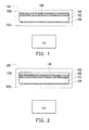
- FIG. 1 is a cross-sectional view of the fingerprint reader in accordance with an embodiment.
- FIG. 2 is a cross-sectional view of the fingerprint reader in accordance with another embodiment.
- FIG. 3 is a cross-sectional view of the fingerprint reader in accordance with yet another embodiment.
- FIG. 4A to FIG. 4E are images in accordance with example 1.
- FIG. 5A to FIG. 5C are images in accordance with example 2.
- FIG. 6A and FIG. 6B are images in accordance with example 3.
- FIG. 7A and FIG. 7B are images in accordance with example 4.
- FIG. 8A and FIG. 8B are images in accordance with example 5.
- FIG. 9A and FIG. 9B are images in accordance with example 6.
- FIG. 1 it shows a fingerprint reader in one embodiment of the present disclosure.
- a major part of the fingerprint reader is a press sheet 100 which includes a transparent substrate 102 , microstructure layer 104 and a diffusion layer 106 .
- the transparent substrate 102 has a first surface 102 a and a second surface 102 b.
- the microstructure layer 104 is disposed on the first surface 102 a of the transparent substrate and could be one of shapes of prismatic (prism), lenticular lens (lenticular), semi-circular dome, pyramid, cylinder and regular polygonal.
- the aforementioned microstructure layer has arrangements of random, period or a combination thereof
- the diffusion layer 106 is disposed on the second surface 102 b of the transparent substrate and includes diffusion particles 108 .
- the aforementioned transparent substrate 102 is made of for instance, polyethylene terephthalate (PET), polycarbonate (PC), polymethyl methacrylate (PMMA), cellulose triacetate (TAC) or any other transparent materials.
- PET polyethylene terephthalate
- PC polycarbonate
- PMMA polymethyl methacrylate
- TAC cellulose triacetate
- the diffusion layer 106 further comprises resin, such as UV curable resin, the mal curable resin and so on.
- the resin includes acrylic, epoxy, polyester, PU, PU acrylic, polysiloxane or a combination thereof Otherwise, uniform distribution of light may cause from the resin and the diffusion particles 108 have the refractive index difference of 0.01 to 1.5.
- the diffusion particles 108 comprise polystyrene, poly methyl acrylate, methyl methacrylate and styrene copolymer, polycarbonate, polyethylene, silicone resins, calcium carbonate, silica, titanium dioxide, or a combination thereof
- the diffusion particles 108 have a particle size of 0.01 ⁇ m to 30.0 ⁇ m. The present disclosure is not limited to this.
- the fingerprint identification and the accuracy should be raised due to the aforementioned diffusion layer 106 , it may cause the haze of press sheet 100 larger than for instance 95%. Moreover, the more amounts of the diffusion particles 108 of the diffusion layer 106 and/or the more thickness of the diffusion layer 106 may make further raising the haze.
- the diffusion layer 106 has the thickness of 1 ⁇ m to 80 ⁇ m or the diffusion particles and the resin have weight ratio of 0.01 to 10.0, and more particular have 0.1 to 2.0.
- FIG. 2 is a cross-sectional view of another embodiment. Using the same elements as the previous embodiment symbols to represent the same or similar components.
- the fingerprint reader includes press sheet 200 which is similar to that of in FIG. 1 , not only includes transparent substrate 102 , microstructure layer 104 and diffusion layer 106 but also includes a protection layer 202 disposed on the diffusion layer 106 .
- the protection layer 202 for instance could be a hard-coat which is coated on the diffusion layer 106 for increasing the lifetime of the press sheet 200 , scratch resistance and so on.
- the hard-coat includes acrylic resin, epoxy resin, polyester, polyurethane (PU), PU acrylic, polysiloxane, acrylic resin with inorganic particles, epoxy with inorganic particles, polysiloxane with inorganic particles, polyester with inorganic particles, PU with inorganic particles, PU acrylic with inorganic particles or a combination thereof.
- the fingerprint reader includes press sheet 200 which is similar to that of in FIG. 2 .
- press sheet 200 which is similar to that of in FIG. 2 .
- the optical imaging apparatus 300 includes a light source 302 and an optic camera lens 304 .
- the optic camera lens 304 is arranged between the light source 302 and the press sheet 200 .
- FIG. 3 shows three light sources 302 in this embodiment, for the present disclosure is not limited to this. Otherwise, the optic camera lens 304 may embed in the diffusion layer 306 for an alternative.
- the measurements were conducted with a haze meter (made by NIPPON DENSHOKU with a trade number of NDH 2000) with the build-in Method 3 which is the standard test of JIS K 7136, ISO 14782.
- the sample was placed with the structure surface faced to light source of the haze meter.
- IPA isopropanol
- diffusion particles manufactured by JX Nippon oil & Energy Corporation, with a trade number NMB-0120C, refraction index of 1.49
- FC4432 fluorosurfactant
- FC4432 diffusion particles
- Toluene, isopropanol, NMB-0120C, fluorosurfactant, and UV glue were mixed and stirred at room temperature for about 2 hours, a mixture (diffusion layer solution) was obtained and had solid content of about 70wt %.
- the NMB-0120C (diffusion particles) and UV glue had weight ratio of 0.3.
- the above mixture was coated on one flat surface of the PET film having a thickness of 90 ⁇ m to 95 ⁇ m which with microlens structure surface opposite to the flat surface to faun a coated PET film. After drying at 80° C. for about 3 minutes, it was cured with UV light to form a dry film with the thickness of 7 ⁇ m as sample 1-1.
- Sample 1-2 to sample 1-4 were prepared same as sample 1-1 with the only difference in sample 1-2 to sample 1-4 were the thickness of dry film of 9 ⁇ m, 13 ⁇ m and 17 ⁇ m respectively.
- Sample 1-5 was prepared same as sample 1-4 except for further coating acrylic PU resin on the dry film with a thickness of 17 ⁇ m, and cured with UV light to form a protective layer with the thickness of 8 ⁇ m.
- Comparative sample 1 was a PET film which one surface had microlens structure.
- a diffusion layer solution was prepared same as example 1.
- the diffusion layer solution was coated on the flat surface of the PET film having the thickness of 155 ⁇ m which with single prism structure opposite to the flat surface to form a coated PET film. After drying at 80° C. for about 3 minutes, it was cured with UV light to form a dry film with the thickness of 16 ⁇ m as sample 2-1.
- Sample 2-2 was prepared same as sample 2-1 except for the thickness for dry film of 16 ⁇ m. Further coated acrylic PU resin on the dry film with a thickness of 16 ⁇ m, and cured with UV light to form a protective layer with the thickness of 8 ⁇ m.
- Comparative sample 2 was a PET film which one surface had prism structure.
- FIG. 5A to FIG. 5C show the imaging for comparative sample 2, sample 2-1 and sample 2-1.
- the imaging identity of comparative sample 2 was bad (X), sample 2-1 and sample 2-1 were good (O).
- the longitudinal direction in FIG. 5A will change as the strip direction of the prism. That is the longitudinal direction is parallel to the strip direction of the prism.
- the strip of the prism turns 90 degrees in FIG. 5A
- the imaging in FIG. 5A to FIG. 5C are also turn 90 degrees.
- LA lauryl acrylate
- MMA toluene
- BPO Benzoyl peroxide
- LA30-MMA70 a solution called LA30-MMA70 was obtained.
- the reaction temperature was set at about 90° C. and the reflux condenser for the temperature was set at 15° C.-25° C.
- the heating method was used heating package.
- the refractive index of the solution LA30-MMA70 was about 1.47.
- Added diffusion particles with the refractive index of 1.59 (manufactured by SEKISUI with a trade number of SBX4) and LA30-MMA70 with the weight ratio of 0.5 to the reactor which had solvent and dispersant then mixed and stirred at room temperature for about 2 hours. After mixing and stirring, a mixture (diffusion layer solution) was obtained and had solid content of about 30.4wt %.
- the above mixture was coated on the flat surface of the PET film having a thickness of 95 ⁇ m which with microlens structure surface opposite to the flat surface to form a coated PET film. After drying at 100° C. for about 3 minutes, a dry film was obtained as sample 3-1.
- Sample 3-2 was prepared same as sample 3-1 except for the coated PE film having a thickness of 155 ⁇ m and one surface of the PET film was prism structure.
- FIG. 6A and FIG. 6B show the fingerprint images for sample 3-1 and sample 3-2. As shown in Table 3 and refer to FIG. 6A to FIG. 6B , both of them have good imaging identity. According to the results, even if one surface of the PET film has different structure, the identification in central region of the fingerprint imaging for coated film was obvious to distinguish.
- Toluene and isopropanol served as a solvent.
- Fluorosurfactant (manufactured by 3M with a trade number of FC4432) served as a dispersant.
- Toluene, isopropanol, titanium oxide, fluorosurfactant, and UV glue (refractive index of 1.58) were mixed and stirred at room temperature for about 2 hours, a mixture (diffusion layer solution) was obtained and had solid content of about 70wt %.
- the titanium oxide and UV glue had weight ratio of 0.1.
- the above mixture was coated on one flat surface of the PET film having a thickness of 90 ⁇ m to 95 ⁇ m which with microlens structure surface opposite to the flat surface to form a coated PET film. After drying at 80° C. for about 3 minutes, it was cured with UV light to form a dry film with the thickness of 12 ⁇ m as sample 4-1. Sample 4-2 was prepared same as sample 4-1, the difference in sample 4-2 was the thickness of the dry film of 17 ⁇ m.
- FIG. 7A and FIG. 7B showed the fingerprint images for sample 4-1 and sample 4-2. As shown in Table 4 and refer to FIG. 7A to FIG. 7B , both of them have good imaging identity.
- IPA isopropanol
- diffusion particles manufactured by JX Nippon oil & Energy Corporation, with a trade number NMB-0120C, refraction index of 1.49
- FC4432 fluorosurfactant
- FC4432 diffusion particles
- Toluene, isopropanol, NMB-0120C, fluorosurfactant, and UV glue were mixed and stirred at room temperature for about 2 hours, a mixture (diffusion layer solution) was obtained and had solid content of about 45wt %.
- the NMB-0120C (diffusion particles) and UV glue had weight ratio of 1.
- the above mixture was coated on one flat surface of the PET film having a thickness of 90 ⁇ m to 95 ⁇ m which with microlens structure surface opposite to the flat surface to form a coated PET film. After drying at 80° C. for about 3 minutes, took it out and curried it with UV light to form a dry film with the thickness of 10 ⁇ m as sample 5-1.
- Sample 5-2 was prepared same as sample 5-1, the difference in sample 5-2 was the thickness of the dry film of 15 ⁇ m.
- FIG. 8A and FIG. 8B showed the fingerprint images for sample 5-1 and sample 5-2. As shown in Table 5 and refer to FIG. 8A to FIG. 8B , both of them have good imaging identity.
- IPA isopropanol
- diffusion particles manufactured by JX Nippon oil & Energy Corporation, with a trade number NMB-0120C, refraction index of 1.49
- FC4432 fluorosurfactant
- FC4432 diffusion particles
- Toluene, isopropanol, NMB-0120C, fluorosurfactant, and UV glue were mixed and stirred at room temperature for about 2 hours, a mixture (diffusion layer solution) was obtained and had solid content of about 30wt %.
- the NMB-0120C (diffusion particles) and UV glue had weight ratio of 2.
Landscapes
- Physics & Mathematics (AREA)
- General Physics & Mathematics (AREA)
- Optics & Photonics (AREA)
- Engineering & Computer Science (AREA)
- Chemical & Material Sciences (AREA)
- Dispersion Chemistry (AREA)
- Human Computer Interaction (AREA)
- Multimedia (AREA)
- Theoretical Computer Science (AREA)
- Image Input (AREA)
- Measurement Of The Respiration, Hearing Ability, Form, And Blood Characteristics Of Living Organisms (AREA)
- Laminated Bodies (AREA)
Abstract
Description
- This application claims the priority benefit of U.S. provisional application Ser. No. 62/067,966, filed on Oct. 23, 2014. The entirety of each of the above-mentioned patent applications is hereby incorporated by reference herein and made a part of this specification.
- The present disclosure relates to a press sheet for fingerprint reader and a fingerprint reader.
- Fingerprints are one of many forms of biometrics used to identify individuals and verify their identities. Fingerprint readers have been gradually incorporated with many electronic products as password security protections such as access control system, and the combination devices with vehicle, notebook computers, mobile phones, flash drives, mouse and keyboard etc. The analysis of fingerprints for matching purposes generally requires the comparison of several features of the print pattern. These include patterns, which are aggregate characteristics of ridges, split, split and join and minutia points, which are unique features found within the patterns.
- Fingerprint reader generally has an optical, capacitive, ultrasonic and thermal induction type, etc. Optical fingerprint reader belongs to the total reflection type, it commonly includes an optical module and an optical imaging apparatus.
- It is difficult and complicated to assemble the total reflection type fingerprint reader. Since people must precisely arrange the optical module and an optical imaging apparatus in the assembly process in order to effectively adjust the angle of the light incident and emergent beams. Furthermore, the emitting source of optical type fingerprint reader is usually a point light source, it easily leads to the blurred image due to uneven distribution of light.
- In accordance with the disclosure, embodiments of the present disclosure are directed to a press sheet for fingerprint reader comprising a transparent substrate, a microstructure layer, and a diffusion layer. The transparent substrate has a first surface and a second surface, and the first surface faces an optical imaging apparatus. The microstructure layer is disposed on the first surface of the transparent substrate. The diffusion layer is disposed on the second surface of the transparent substrate, and comprises a plurality of diffusion particles.
- In one embodiment, the aforementioned diffusion layer includes resin. The resin comprises acrylic, epoxy resin, polyester, polyurethane (PU), PU acrylic, polysiloxane or a combination thereof.
- According to the disclosure, the resin and the diffusion particles have a refractive index difference of 0.01 to 1.5. The diffusion particles and the resin have a weight ratio of 0.01 to 2.0.
- The aforementioned diffusion particles include polystyrene, poly methyl acrylate, methyl methacrylate and styrene copolymer, polycarbonate, polyethylene, silicone resins, calcium carbonate, silica, titanium dioxide, or a combination thereof.
- One embodiment of the disclosure, the diffusion particles have a particle size of 0.01 μm to 30.0 μm.
- The aforementioned diffusion layer has a thickness of 1 μm to 80 μm in one embodiment of the disclosure.
- In one embodiment of the disclosure, the materials of transparent substrate include polyethylene terephthalate (PET), polycarbonate (PC), polymethyl methacrylate (PMMA), and cellulose triacetate (TAC).
- In one embodiment of the disclosure, the microstructure layer has at least one of the structure of prismatic (prism), lenticular lens (lenticular), semi-circular dome, pyramid, cylinder or regular polygonal.
- The aforementioned microstructure has at least an arrangement of random or period in one embodiment of the disclosure.
- According to the disclosure, the transparent substrate and the microstructure layer are integrated.
- In the present disclosure, the press sheet further comprises a protective layer which is disposed on the diffusion layer. The protective layer could be a hard coating.
- The present disclosure also relates to a fingerprint reader. The fingerprint reader comprises the aforementioned press sheet and at least one optical imaging apparatus. In one embodiment of the disclosure, the optical imaging apparatus includes light source and an optic camera lens, and the optic camera lens is arranged between the light source and the press sheet.
- The accompanying drawings are included to provide a further understanding of the disclosure, and are incorporated in and constitute a part of this specification. The drawings illustrate embodiments of the disclosure and, together with the description, serve to explain the principles of the disclosure.
-
FIG. 1 is a cross-sectional view of the fingerprint reader in accordance with an embodiment. -
FIG. 2 is a cross-sectional view of the fingerprint reader in accordance with another embodiment. -
FIG. 3 is a cross-sectional view of the fingerprint reader in accordance with yet another embodiment. -
FIG. 4A toFIG. 4E are images in accordance with example 1. -
FIG. 5A toFIG. 5C are images in accordance with example 2. -
FIG. 6A andFIG. 6B are images in accordance with example 3. -
FIG. 7A andFIG. 7B are images in accordance with example 4. -
FIG. 8A andFIG. 8B are images in accordance with example 5. -
FIG. 9A andFIG. 9B are images in accordance with example 6. - The disclosure will now be described with reference to the accompanying figures. It is to be understood that the specific illustrated in the attached figures and described in the following description is simply an exemplary embodiment of the present disclosure. This description is made for the purpose of illustrating the general principles of the disclosure and should not be taken in a limiting sense. The scope of the disclosure is best determined by reference to the appended claims
- Referring to
FIG. 1 , it shows a fingerprint reader in one embodiment of the present disclosure. A major part of the fingerprint reader is apress sheet 100 which includes atransparent substrate 102,microstructure layer 104 and adiffusion layer 106. Thetransparent substrate 102 has afirst surface 102 a and asecond surface 102 b. Themicrostructure layer 104 is disposed on thefirst surface 102 a of the transparent substrate and could be one of shapes of prismatic (prism), lenticular lens (lenticular), semi-circular dome, pyramid, cylinder and regular polygonal. The aforementioned microstructure layer has arrangements of random, period or a combination thereof Thediffusion layer 106 is disposed on thesecond surface 102 b of the transparent substrate and includesdiffusion particles 108. - The aforementioned
transparent substrate 102 is made of for instance, polyethylene terephthalate (PET), polycarbonate (PC), polymethyl methacrylate (PMMA), cellulose triacetate (TAC) or any other transparent materials. As thefirst surface 102 a of thetransparent substrate 102 faces toward to anoptical imaging apparatus 110, due to thediffusion particles 108 of thediffusion layer 106 may cause uniform distribution of light. In an embodiment of the disclosure, thediffusion layer 106 further comprises resin, such as UV curable resin, the mal curable resin and so on. Generally speaking, the resin includes acrylic, epoxy, polyester, PU, PU acrylic, polysiloxane or a combination thereof Otherwise, uniform distribution of light may cause from the resin and thediffusion particles 108 have the refractive index difference of 0.01 to 1.5. In an embodiment of the present disclosure, thediffusion particles 108 comprise polystyrene, poly methyl acrylate, methyl methacrylate and styrene copolymer, polycarbonate, polyethylene, silicone resins, calcium carbonate, silica, titanium dioxide, or a combination thereof Thediffusion particles 108 have a particle size of 0.01 μm to 30.0 μm. The present disclosure is not limited to this. - The fingerprint identification and the accuracy should be raised due to the
aforementioned diffusion layer 106, it may cause the haze ofpress sheet 100 larger than for instance 95%. Moreover, the more amounts of thediffusion particles 108 of thediffusion layer 106 and/or the more thickness of thediffusion layer 106 may make further raising the haze. For example, thediffusion layer 106 has the thickness of 1 μm to 80 μm or the diffusion particles and the resin have weight ratio of 0.01 to 10.0, and more particular have 0.1 to 2.0. -
FIG. 2 is a cross-sectional view of another embodiment. Using the same elements as the previous embodiment symbols to represent the same or similar components. - Referring to
FIG. 2 , in this embodiment the fingerprint reader includespress sheet 200 which is similar to that of inFIG. 1 , not only includestransparent substrate 102,microstructure layer 104 anddiffusion layer 106 but also includes aprotection layer 202 disposed on thediffusion layer 106. Theprotection layer 202, for instance could be a hard-coat which is coated on thediffusion layer 106 for increasing the lifetime of thepress sheet 200, scratch resistance and so on. The hard-coat includes acrylic resin, epoxy resin, polyester, polyurethane (PU), PU acrylic, polysiloxane, acrylic resin with inorganic particles, epoxy with inorganic particles, polysiloxane with inorganic particles, polyester with inorganic particles, PU with inorganic particles, PU acrylic with inorganic particles or a combination thereof. - Referring to
FIG. 3 , in this embodiment the fingerprint reader includespress sheet 200 which is similar to that of inFIG. 2 . Using the same elements as the previous embodiment symbols to represent the same or similar components. There is anoptical imaging apparatus 300 arranged toward the press sheet. Theoptical imaging apparatus 300 includes alight source 302 and anoptic camera lens 304. Theoptic camera lens 304 is arranged between thelight source 302 and thepress sheet 200. AlthoughFIG. 3 shows threelight sources 302 in this embodiment, for the present disclosure is not limited to this. Otherwise, theoptic camera lens 304 may embed in thediffusion layer 306 for an alternative. - Below, exemplary embodiments will be described to verify the efficacy of the present disclosure, but the disclosure is not limited to the exemplary embodiments set forth herein.
- Haze Measurement
- The measurements were conducted with a haze meter (made by NIPPON DENSHOKU with a trade number of NDH 2000) with the build-in Method 3 which is the standard test of JIS K 7136, ISO 14782. The sample was placed with the structure surface faced to light source of the haze meter.
- Toluene and a little amount of isopropanol served as a solvent. The isopropanol (IPA) and diffusion particles (manufactured by JX Nippon oil & Energy Corporation, with a trade number NMB-0120C, refraction index of 1.49) had weight ratio of 0.03 (IPA/NMB-0120C=0.03). Fluorosurfactant (manufactured by 3M with a trade number of FC4432) served as a dispersant. The fluorosurfactant (FC4432) and diffusion particles NMB-0120C had weight ratio of 0.012 (FC4432/NMB-0120C=0.012). Toluene, isopropanol, NMB-0120C, fluorosurfactant, and UV glue (refractive index of 1.60) were mixed and stirred at room temperature for about 2 hours, a mixture (diffusion layer solution) was obtained and had solid content of about 70wt %. The NMB-0120C (diffusion particles) and UV glue had weight ratio of 0.3.
- The above mixture was coated on one flat surface of the PET film having a thickness of 90 μm to 95 μm which with microlens structure surface opposite to the flat surface to faun a coated PET film. After drying at 80° C. for about 3 minutes, it was cured with UV light to form a dry film with the thickness of 7 μm as sample 1-1.
- Sample 1-2 to sample 1-4 were prepared same as sample 1-1 with the only difference in sample 1-2 to sample 1-4 were the thickness of dry film of 9 μm, 13 μm and 17 μm respectively.
- Sample 1-5 was prepared same as sample 1-4 except for further coating acrylic PU resin on the dry film with a thickness of 17 μm, and cured with UV light to form a protective layer with the thickness of 8 μm.
- Comparative sample 1 was a PET film which one surface had microlens structure.
- The haze measured and tabulated in Table 1.
-
TABLE 1 Haze Thickness of for diffusion Imaging diffusion layer layer Total Haze identity Comparative No coating layer 94.39% X sample 1 Sample 1-1 7 μm 78.56% 97.78% Δ Sample 1-2 9 μm 88.62% 98.38% ◯ Sample 1-3 13 μm 93.62% 98.68% ◯ Sample 1-4 17 μm 97.24% 98.92% ◯ Sample 1-5 17 μm 97.24% 99.05% ◯ - As shown in Table 1 and refer to
FIG. 4A toFIG. 4E , the imaging identity of comparative sample 1 was bad (X), sample 1-1 was normal (A), and sample 1-2 to sample 1-5 were all good (O). - According to Table 1 and
FIG. 4A toFIG. 4E , it shows that no identified imaging was found in the central region of the one-side microlens structure film (comparative sample 1). The central region of the fingerprint imaging with total haze of 97.78% was unobvious. The identification in central region of the fingerprint imaging for the total haze more than 98% was obvious and easy to distinguish. - A diffusion layer solution was prepared same as example 1. The diffusion layer solution was coated on the flat surface of the PET film having the thickness of 155 μm which with single prism structure opposite to the flat surface to form a coated PET film. After drying at 80° C. for about 3 minutes, it was cured with UV light to form a dry film with the thickness of 16 μm as sample 2-1.
- Sample 2-2 was prepared same as sample 2-1 except for the thickness for dry film of 16 μm. Further coated acrylic PU resin on the dry film with a thickness of 16 μm, and cured with UV light to form a protective layer with the thickness of 8 μm.
- Comparative sample 2 was a PET film which one surface had prism structure.
- The haze measured and tabulated in Table 2.
-
TABLE 2 Thickness of Haze for diffusion Imaging diffusion layer layer Total Haze identity Comparative No coating layer — X sample 2 (with one prism structure surface) Sample 2-1 16 μm 97.37% — ◯ Sample 2-2 16 μm 88.62% — ◯ (with hard coating) -
FIG. 5A toFIG. 5C show the imaging for comparative sample 2, sample 2-1 and sample 2-1. As shown in Table 2 and refer toFIG. 5A toFIG. 5C , the imaging identity of comparative sample 2 was bad (X), sample 2-1 and sample 2-1 were good (O). The longitudinal direction inFIG. 5A will change as the strip direction of the prism. That is the longitudinal direction is parallel to the strip direction of the prism. For instance, the strip of the prism turns 90 degrees inFIG. 5A , and the imaging inFIG. 5A toFIG. 5C are also turn 90 degrees. In addition, it is meaningless to measure the total haze since when light source irradiates the prism structure surface of the dry film, most of the light is reflected so the transmitted light is very weak that may cause the calculation for haze is distorted. - According to Table 2 and
FIG. 5A toFIG. 5C , it shows that no identified imaging was found in the central region of the plain prism structure film. The identification in central region of the fingerprint imaging for coated film was obvious to distinguish. - Added lauryl acrylate (LA), MMA, toluene, Benzoyl peroxide (BPO) (IUPAC diphenylperoxyanhydride) with the weight ratio of 3:7:15:0.3 to the closed reactor having reflux condenser, mixed with stirrer for 10 minutes in Nitrogen atmosphere then stopped introducing Nitrogen gas and kept stirring for 10 hours, a solution called LA30-MMA70 was obtained. In the aforementioned reaction, the reaction temperature was set at about 90° C. and the reflux condenser for the temperature was set at 15° C.-25° C. The heating method was used heating package. The refractive index of the solution LA30-MMA70 was about 1.47.
- Toluene and a little amount of isopropanol solution served as a solvent. The isopropanol solution was prepared with isopropanol and NMB-0120C for the weight ratio of 0.03 (IPA/NMB0120C=0.03). Fluorosurfactant (manufactured by 3M with a trade number of FC4432) served as a dispersant of (FC4432/SBX4=0.06 wt %). Added diffusion particles with the refractive index of 1.59 (manufactured by SEKISUI with a trade number of SBX4) and LA30-MMA70 with the weight ratio of 0.5 to the reactor which had solvent and dispersant then mixed and stirred at room temperature for about 2 hours. After mixing and stirring, a mixture (diffusion layer solution) was obtained and had solid content of about 30.4wt %.
- The above mixture was coated on the flat surface of the PET film having a thickness of 95 μm which with microlens structure surface opposite to the flat surface to form a coated PET film. After drying at 100° C. for about 3 minutes, a dry film was obtained as sample 3-1.
- Sample 3-2 was prepared same as sample 3-1 except for the coated PE film having a thickness of 155 μm and one surface of the PET film was prism structure.
- After drying at 100° C. for about 3 minutes, a dry film was obtained with the thickness of 14 μm.
- The haze measured and tabulated in Table 3.
-
TABLE 3 Thickness of Haze for diffusion Total Imaging diffusion layer layer Haze identity Sample 3-1 14 μm 96.97% 99.13% ◯ Sample 3-2 14 μm 96.97% — ◯ -
FIG. 6A andFIG. 6B show the fingerprint images for sample 3-1 and sample 3-2. As shown in Table 3 and refer toFIG. 6A toFIG. 6B , both of them have good imaging identity. According to the results, even if one surface of the PET film has different structure, the identification in central region of the fingerprint imaging for coated film was obvious to distinguish. - Preparation of Diffusion Layer Solution
- Toluene and isopropanol served as a solvent. The isopropanol (IPA) and titanium oxide (TiO2, manufactured by DuPont with a trade number R350) had weight ratio of 0.0435 (IPA/TiO2=0.0435). Fluorosurfactant (manufactured by 3M with a trade number of FC4432) served as a dispersant. The fluorosurfactant (FC4432) and titanium oxide (TiO2, manufactured by DuPont with a trade number R350, refractive index of 2.6) had weight ratio of 0.012 (FC4432/TiO2=0.012). Toluene, isopropanol, titanium oxide, fluorosurfactant, and UV glue (refractive index of 1.58) were mixed and stirred at room temperature for about 2 hours, a mixture (diffusion layer solution) was obtained and had solid content of about 70wt %. The titanium oxide and UV glue had weight ratio of 0.1.
- The above mixture was coated on one flat surface of the PET film having a thickness of 90 μm to 95 μm which with microlens structure surface opposite to the flat surface to form a coated PET film. After drying at 80° C. for about 3 minutes, it was cured with UV light to form a dry film with the thickness of 12 μm as sample 4-1. Sample 4-2 was prepared same as sample 4-1, the difference in sample 4-2 was the thickness of the dry film of 17 μm.
- The haze measured and tabulated in Table 4.
-
TABLE 4 Thickness of Haze for Imaging diffusion layer diffusion layer Total Haze identity Sample 4-1 12 μm 75.79% 98.92% ◯ Sample 4-2 17 μm 78.54% 99.02% ◯ -
FIG. 7A andFIG. 7B showed the fingerprint images for sample 4-1 and sample 4-2. As shown in Table 4 and refer toFIG. 7A toFIG. 7B , both of them have good imaging identity. - Preparation of Diffusion Layer Solution
- Toluene and a little amount of isopropanol served as a solvent. The isopropanol (IPA) and diffusion particles (manufactured by JX Nippon oil & Energy Corporation, with a trade number NMB-0120C, refraction index of 1.49) had weight ratio of 0.03 (IPA/NMB-0120C=0.03). Fluorosurfactant (manufactured by 3M with a trade number of FC4432) served as a dispersant. The fluorosurfactant (FC4432) and diffusion particles NMB-0120C had weight ratio of 0.012 (FC4432/NMB-0120C=0.012). Toluene, isopropanol, NMB-0120C, fluorosurfactant, and UV glue (refractive index of 1.58) were mixed and stirred at room temperature for about 2 hours, a mixture (diffusion layer solution) was obtained and had solid content of about 45wt %. The NMB-0120C (diffusion particles) and UV glue had weight ratio of 1.
- The above mixture was coated on one flat surface of the PET film having a thickness of 90 μm to 95 μm which with microlens structure surface opposite to the flat surface to form a coated PET film. After drying at 80° C. for about 3 minutes, took it out and curried it with UV light to form a dry film with the thickness of 10 μm as sample 5-1.
- Sample 5-2 was prepared same as sample 5-1, the difference in sample 5-2 was the thickness of the dry film of 15 μm.
- The haze measured and tabulated in Table 5.
-
TABLE 5 Thickness of Haze for Imaging diffusion layer diffusion layer Total Haze identity Sample 5-1 10 μm 96.81% 99.06% ◯ Sample 5-2 15 μm 98.30% 99.13% ◯ -
FIG. 8A andFIG. 8B showed the fingerprint images for sample 5-1 and sample 5-2. As shown in Table 5 and refer toFIG. 8A toFIG. 8B , both of them have good imaging identity. - Example 6
- Preparation of Diffusion Layer Solution
- Toluene and a little amount of isopropanol served as a solvent. The isopropanol (IPA) and diffusion particles (manufactured by JX Nippon oil & Energy Corporation, with a trade number NMB-0120C, refraction index of 1.49) had weight ratio of 0.03 (IPA/NMB-0120C=0.03). Fluorosurfactant (manufactured by 3M with a trade number of FC4432) served as a dispersant. The fluorosurfactant (FC4432) and diffusion particles NMB-0120C had weight ratio of 0.012 (FC4432/NMB-0120C=0.012). Toluene, isopropanol, NMB-0120C, fluorosurfactant, and UV glue (refractive index of 1.58) were mixed and stirred at room temperature for about 2 hours, a mixture (diffusion layer solution) was obtained and had solid content of about 30wt %. The NMB-0120C (diffusion particles) and UV glue had weight ratio of 2.
- The above mixture was coated on one flat surface of the PET film having a thickness of 90 μm to 95 μm which with microlens structure surface opposite to the flat surface to form a coated PET film. After drying at 80° C. for about 3 minutes, it was cured with UV light to form a dry film with the thickness of 5 μm as sample 6-1.
- Sample 6-2 was prepared same as sample 6-1, the difference in sample 6-2 was the thickness of the dry film of 9 μm.
- The haze measured and tabulated in Table 6.
-
TABLE 6 Thickness of Haze for Imaging diffusion layer diffusion layer Total Haze identity Sample 6-1 5 μm 84.01% 98.52% ◯ Sample 6-2 9 μm 98.09% 99.21% ◯ -
FIG. 9A andFIG. 9B showed the fingerprint images for sample 6-1 and sample 6-2. Both of them had good imaging identity. - It will be apparent to those skilled in the art that various modifications and variations can be made to the disclosed methods and materials. It is intended that the specification and examples be considered as exemplary only, with the true scope of the disclosure being indicated by the following claims and their equivalents.
Claims (16)
Priority Applications (2)
| Application Number | Priority Date | Filing Date | Title |
|---|---|---|---|
| US14/822,891 US10061964B2 (en) | 2014-10-23 | 2015-08-10 | Press sheet for fingerprint reader and fingerprint reader |
| US16/027,286 US20180330140A1 (en) | 2014-10-23 | 2018-07-04 | Fingerprint identification apparatus |
Applications Claiming Priority (2)
| Application Number | Priority Date | Filing Date | Title |
|---|---|---|---|
| US201462067966P | 2014-10-23 | 2014-10-23 | |
| US14/822,891 US10061964B2 (en) | 2014-10-23 | 2015-08-10 | Press sheet for fingerprint reader and fingerprint reader |
Related Child Applications (1)
| Application Number | Title | Priority Date | Filing Date |
|---|---|---|---|
| US16/027,286 Continuation-In-Part US20180330140A1 (en) | 2014-10-23 | 2018-07-04 | Fingerprint identification apparatus |
Publications (2)
| Publication Number | Publication Date |
|---|---|
| US20160117543A1 true US20160117543A1 (en) | 2016-04-28 |
| US10061964B2 US10061964B2 (en) | 2018-08-28 |
Family
ID=55792237
Family Applications (1)
| Application Number | Title | Priority Date | Filing Date |
|---|---|---|---|
| US14/822,891 Active 2036-09-25 US10061964B2 (en) | 2014-10-23 | 2015-08-10 | Press sheet for fingerprint reader and fingerprint reader |
Country Status (3)
| Country | Link |
|---|---|
| US (1) | US10061964B2 (en) |
| CN (1) | CN105549134B (en) |
| TW (1) | TWI552091B (en) |
Cited By (10)
| Publication number | Priority date | Publication date | Assignee | Title |
|---|---|---|---|---|
| US20170177921A1 (en) * | 2015-12-22 | 2017-06-22 | 3M Innovative Properties Company | Fingerprint imaging systems comprising self-wetting adhesive, films and methods |
| CN107688804A (en) * | 2016-08-05 | 2018-02-13 | 金佶科技股份有限公司 | Image capturing device |
| TWI630502B (en) * | 2016-08-05 | 2018-07-21 | 金佶科技股份有限公司 | Image capture apparatus |
| US10460188B2 (en) | 2014-08-26 | 2019-10-29 | Gingy Technology Inc. | Bio-sensing apparatus |
| US10613256B2 (en) * | 2017-08-11 | 2020-04-07 | Industrial Technology Research Institute | Biometric device |
| US10699098B2 (en) | 2017-12-12 | 2020-06-30 | Industrial Technology Research Institute | Fingerprint recognition device |
| US10713521B2 (en) | 2016-08-05 | 2020-07-14 | Gingy Technology Inc. | Image capturing apparatus and manufacturing method thereof |
| US10713465B2 (en) | 2016-08-05 | 2020-07-14 | Gingy Technology Inc. | Image capture apparatus |
| KR20210034914A (en) * | 2019-09-23 | 2021-03-31 | 주식회사 엘엠에스 | Optical film for fingerprinting |
| US12109771B2 (en) | 2019-02-25 | 2024-10-08 | Ams Sensors Singapore Pte. Ltd. | Manufacture of optical diffusers composed of reflowable materials |
Families Citing this family (6)
| Publication number | Priority date | Publication date | Assignee | Title |
|---|---|---|---|---|
| TWI664578B (en) * | 2016-08-05 | 2019-07-01 | Gingy Technology Inc. | Image capturing apparatus and manufacturing method thereof |
| CN107273787A (en) * | 2017-03-28 | 2017-10-20 | 敦捷光电股份有限公司 | Infrared-penetrable optical fingerprint sensing device and manufacturing method thereof |
| WO2019032590A1 (en) * | 2017-08-09 | 2019-02-14 | The Board Of Trustees Of The Leland Stanford Junior University | Interactive biometric touch scanner |
| TWI652626B (en) | 2017-08-11 | 2019-03-01 | 財團法人工業技術研究院 | Biometric device |
| CN111435213B (en) | 2019-01-11 | 2021-12-31 | 财团法人工业技术研究院 | Imaging module and biometric device using the same |
| US11783621B2 (en) | 2021-11-19 | 2023-10-10 | Gingy Technology Inc. | Optical fingerprint imaging device |
Family Cites Families (14)
| Publication number | Priority date | Publication date | Assignee | Title |
|---|---|---|---|---|
| US6091838A (en) | 1998-06-08 | 2000-07-18 | E.L. Specialists, Inc. | Irradiated images described by electrical contact |
| US7526109B2 (en) * | 2003-11-26 | 2009-04-28 | Microsoft Corporation | Fingerprint scanner with translating scan head |
| JP2009180895A (en) * | 2008-01-30 | 2009-08-13 | Sumitomo Chemical Co Ltd | Light diffusing plate, surface light source device, and liquid crystal display device |
| TWI382349B (en) * | 2009-01-07 | 2013-01-11 | Gingy Technology Inc | Optical light guide module for optical fingerprint identification system |
| TWI382353B (en) | 2009-02-19 | 2013-01-11 | Gingy Technology Inc | Optical Fingerprint Identification System |
| TWI382350B (en) * | 2009-02-19 | 2013-01-11 | Gingy Technology Inc | Optical Fingerprint Identification System |
| CN102682280B (en) * | 2009-02-25 | 2013-06-05 | 金佶科技股份有限公司 | Optical fingerprint identification system |
| KR200462271Y1 (en) * | 2010-10-28 | 2012-09-03 | 징이 테크놀러지 아이엔씨. | Optical fingerprint recognition system |
| TWI461988B (en) * | 2011-06-15 | 2014-11-21 | Pixart Imaging Inc | Optical touch device |
| TWI444904B (en) | 2011-06-24 | 2014-07-11 | Gingy Technology Inc | Finger print identification device |
| TWI450201B (en) | 2011-08-05 | 2014-08-21 | Gingy Technology Inc | Finger board |
| TWI456510B (en) * | 2011-08-24 | 2014-10-11 | Gingy Technology Inc | Fingerprint touch panel |
| DE102013106105A1 (en) * | 2013-06-12 | 2014-12-31 | Dan Hossu | A method of optically capturing a fingerprint or an object and apparatus having at least one screen |
| US20160092718A1 (en) * | 2014-07-16 | 2016-03-31 | Eric Dean Jensen | Fingerprint sensor |
-
2015
- 2015-05-26 TW TW104116820A patent/TWI552091B/en active
- 2015-08-07 CN CN201510481893.0A patent/CN105549134B/en active Active
- 2015-08-10 US US14/822,891 patent/US10061964B2/en active Active
Cited By (16)
| Publication number | Priority date | Publication date | Assignee | Title |
|---|---|---|---|---|
| US10460188B2 (en) | 2014-08-26 | 2019-10-29 | Gingy Technology Inc. | Bio-sensing apparatus |
| US10282583B2 (en) * | 2015-12-22 | 2019-05-07 | Gemalto Sa | Fingerprint imaging systems comprising self-wetting adhesive, films and methods |
| US20170177921A1 (en) * | 2015-12-22 | 2017-06-22 | 3M Innovative Properties Company | Fingerprint imaging systems comprising self-wetting adhesive, films and methods |
| US10713521B2 (en) | 2016-08-05 | 2020-07-14 | Gingy Technology Inc. | Image capturing apparatus and manufacturing method thereof |
| US10356296B2 (en) | 2016-08-05 | 2019-07-16 | Gingy Technology Inc. | Light guide for finger print reader |
| TWI630502B (en) * | 2016-08-05 | 2018-07-21 | 金佶科技股份有限公司 | Image capture apparatus |
| CN107688804A (en) * | 2016-08-05 | 2018-02-13 | 金佶科技股份有限公司 | Image capturing device |
| US10713465B2 (en) | 2016-08-05 | 2020-07-14 | Gingy Technology Inc. | Image capture apparatus |
| US10613256B2 (en) * | 2017-08-11 | 2020-04-07 | Industrial Technology Research Institute | Biometric device |
| US10830926B2 (en) * | 2017-08-11 | 2020-11-10 | Industrial Technology Research Institute | Biometric device |
| US10699098B2 (en) | 2017-12-12 | 2020-06-30 | Industrial Technology Research Institute | Fingerprint recognition device |
| US11354929B2 (en) | 2017-12-12 | 2022-06-07 | Industrial Technology Research Institute | Fingerprint recognition device |
| US12109771B2 (en) | 2019-02-25 | 2024-10-08 | Ams Sensors Singapore Pte. Ltd. | Manufacture of optical diffusers composed of reflowable materials |
| KR20210034914A (en) * | 2019-09-23 | 2021-03-31 | 주식회사 엘엠에스 | Optical film for fingerprinting |
| WO2021060708A1 (en) * | 2019-09-23 | 2021-04-01 | 주식회사 엘엠에스 | Optical film for fingerprint recognition |
| KR102250556B1 (en) * | 2019-09-23 | 2021-05-12 | 주식회사 엘엠에스 | Optical film for fingerprinting |
Also Published As
| Publication number | Publication date |
|---|---|
| US10061964B2 (en) | 2018-08-28 |
| TWI552091B (en) | 2016-10-01 |
| TW201616393A (en) | 2016-05-01 |
| CN105549134A (en) | 2016-05-04 |
| CN105549134B (en) | 2019-03-15 |
Similar Documents
| Publication | Publication Date | Title |
|---|---|---|
| US10061964B2 (en) | Press sheet for fingerprint reader and fingerprint reader | |
| KR102756034B1 (en) | Optical films and image display devices | |
| TWI673513B (en) | Anti reflection film, display device, method for selecting anti reflection flim for display device | |
| JP5179229B2 (en) | Laser pointer visibility improving film, polarizing plate, image display device, and laser pointer display method | |
| KR20170020370A (en) | Layered body for optical member and image display device | |
| TWI647488B (en) | Optical components and their manufacturing methods, as well as window components and building materials | |
| KR20200064091A (en) | Optical film and image display device | |
| US20180149792A1 (en) | Flat panel display embedding optical imaging sensor | |
| KR20080033859A (en) | Surface material for high precision display, high precision display and high precision touch panel provided with it | |
| JP2008180798A (en) | Pattern printing transparent sheet | |
| US20150118455A1 (en) | Intermediate base material film and touch panel sensor | |
| TWI591372B (en) | Surface protection film, capacitive touch panel and image display apparatus | |
| TW201001444A (en) | Transparent electrically conductive film and touch panel including the same | |
| CN113227889B (en) | Texture recognition device and display device | |
| US20160003984A1 (en) | Laminated film and display device | |
| TWI702414B (en) | Optical film and display device with touch panel | |
| CN111164464A (en) | Anti-glare film and display device using same | |
| CN112130239A (en) | Diffusers, backlight modules, liquid crystal display devices and information equipment | |
| Kumar et al. | Unclonable Anti‐Counterfeiting Labels Based on Microlens Arrays and Luminescent Microparticles | |
| JP2015075886A (en) | Laminate and touch panel sensor | |
| KR101090495B1 (en) | Light Diffusion Film for Light Emitting Diodes | |
| US20230016838A1 (en) | Resin layer, optical film, and image displaying device | |
| JP2015178177A (en) | Intermediate substrate film, intermediate substrate film with low refractive index layer, and touch panel sensor | |
| JP5549967B1 (en) | Conductive film and touch panel sensor | |
| JP2015036867A (en) | Intermediate base material film for touch panel, lamination film for touch panel, and touch panel sensor |
Legal Events
| Date | Code | Title | Description |
|---|---|---|---|
| AS | Assignment |
Owner name: INDUSTRIAL TECHNOLOGY RESEARCH INSTITUTE, TAIWAN Free format text: ASSIGNMENT OF ASSIGNORS INTEREST;ASSIGNORS:HUANG, HSIAO-FENG;CHEN, PING-CHEN;CHIANG, CHUN-CHEN;AND OTHERS;REEL/FRAME:036324/0489 Effective date: 20150720 Owner name: GINGYTECH TECHNOLOGY INC., TAIWAN Free format text: ASSIGNMENT OF ASSIGNORS INTEREST;ASSIGNORS:HUANG, HSIAO-FENG;CHEN, PING-CHEN;CHIANG, CHUN-CHEN;AND OTHERS;REEL/FRAME:036324/0489 Effective date: 20150720 |
|
| AS | Assignment |
Owner name: INDUSTRIAL TECHNOLOGY RESEARCH INSTITUTE, TAIWAN Free format text: CORRECTIVE ASSIGNMENT TO CORRECT THE 2ND ASSIGNEE NAME PREVIOUSLY RECORDED AT REEL: 036324 FRAME: 0489. ASSIGNOR(S) HEREBY CONFIRMS THE ASSIGNMENT;ASSIGNORS:HUANG, HSIAO-FENG;CHEN, PING-CHEN;CHIANG, CHUN-CHEN;AND OTHERS;REEL/FRAME:039688/0504 Effective date: 20150720 Owner name: GINGY TECHNOLOGY INC., TAIWAN Free format text: CORRECTIVE ASSIGNMENT TO CORRECT THE 2ND ASSIGNEE NAME PREVIOUSLY RECORDED AT REEL: 036324 FRAME: 0489. ASSIGNOR(S) HEREBY CONFIRMS THE ASSIGNMENT;ASSIGNORS:HUANG, HSIAO-FENG;CHEN, PING-CHEN;CHIANG, CHUN-CHEN;AND OTHERS;REEL/FRAME:039688/0504 Effective date: 20150720 |
|
| STCF | Information on status: patent grant |
Free format text: PATENTED CASE |
|
| MAFP | Maintenance fee payment |
Free format text: PAYMENT OF MAINTENANCE FEE, 4TH YEAR, LARGE ENTITY (ORIGINAL EVENT CODE: M1551); ENTITY STATUS OF PATENT OWNER: LARGE ENTITY Year of fee payment: 4 |
|
| MAFP | Maintenance fee payment |
Free format text: PAYMENT OF MAINTENANCE FEE, 8TH YEAR, LARGE ENTITY (ORIGINAL EVENT CODE: M1552); ENTITY STATUS OF PATENT OWNER: LARGE ENTITY Year of fee payment: 8 |