US20150288288A1 - Isolated power supply circuit with programmable function and control method thereof - Google Patents
Isolated power supply circuit with programmable function and control method thereof Download PDFInfo
- Publication number
- US20150288288A1 US20150288288A1 US14/676,268 US201514676268A US2015288288A1 US 20150288288 A1 US20150288288 A1 US 20150288288A1 US 201514676268 A US201514676268 A US 201514676268A US 2015288288 A1 US2015288288 A1 US 2015288288A1
- Authority
- US
- United States
- Prior art keywords
- signal
- circuit
- output voltage
- current
- programmable
- Prior art date
- Legal status (The legal status is an assumption and is not a legal conclusion. Google has not performed a legal analysis and makes no representation as to the accuracy of the status listed.)
- Granted
Links
- 238000000034 method Methods 0.000 title claims abstract description 19
- 238000007599 discharging Methods 0.000 claims abstract description 53
- 230000000740 bleeding effect Effects 0.000 claims abstract description 46
- 230000007704 transition Effects 0.000 claims abstract description 27
- 238000004804 winding Methods 0.000 claims description 75
- 238000006243 chemical reaction Methods 0.000 claims description 5
- 238000010168 coupling process Methods 0.000 claims description 2
- 238000005859 coupling reaction Methods 0.000 claims description 2
- 239000003990 capacitor Substances 0.000 description 17
- 102100029768 Histone-lysine N-methyltransferase SETD1A Human genes 0.000 description 11
- 101000865038 Homo sapiens Histone-lysine N-methyltransferase SETD1A Proteins 0.000 description 11
- 101150117538 Set2 gene Proteins 0.000 description 10
- 238000004891 communication Methods 0.000 description 10
- 101100218322 Arabidopsis thaliana ATXR3 gene Proteins 0.000 description 9
- 102100032742 Histone-lysine N-methyltransferase SETD2 Human genes 0.000 description 9
- 101100149326 Homo sapiens SETD2 gene Proteins 0.000 description 9
- LZHSWRWIMQRTOP-UHFFFAOYSA-N N-(furan-2-ylmethyl)-3-[4-[methyl(propyl)amino]-6-(trifluoromethyl)pyrimidin-2-yl]sulfanylpropanamide Chemical compound CCCN(C)C1=NC(=NC(=C1)C(F)(F)F)SCCC(=O)NCC2=CC=CO2 LZHSWRWIMQRTOP-UHFFFAOYSA-N 0.000 description 9
- 101100533304 Plasmodium falciparum (isolate 3D7) SETVS gene Proteins 0.000 description 9
- 238000010586 diagram Methods 0.000 description 6
- 230000007423 decrease Effects 0.000 description 2
- 238000012986 modification Methods 0.000 description 2
- 230000004048 modification Effects 0.000 description 2
- 229910044991 metal oxide Inorganic materials 0.000 description 1
- 150000004706 metal oxides Chemical class 0.000 description 1
- 239000004065 semiconductor Substances 0.000 description 1
Images


Classifications
-
- H—ELECTRICITY
- H02—GENERATION; CONVERSION OR DISTRIBUTION OF ELECTRIC POWER
- H02M—APPARATUS FOR CONVERSION BETWEEN AC AND AC, BETWEEN AC AND DC, OR BETWEEN DC AND DC, AND FOR USE WITH MAINS OR SIMILAR POWER SUPPLY SYSTEMS; CONVERSION OF DC OR AC INPUT POWER INTO SURGE OUTPUT POWER; CONTROL OR REGULATION THEREOF
- H02M3/00—Conversion of DC power input into DC power output
- H02M3/22—Conversion of DC power input into DC power output with intermediate conversion into AC
- H02M3/24—Conversion of DC power input into DC power output with intermediate conversion into AC by static converters
- H02M3/28—Conversion of DC power input into DC power output with intermediate conversion into AC by static converters using discharge tubes with control electrode or semiconductor devices with control electrode to produce the intermediate AC
- H02M3/325—Conversion of DC power input into DC power output with intermediate conversion into AC by static converters using discharge tubes with control electrode or semiconductor devices with control electrode to produce the intermediate AC using devices of a triode or a transistor type requiring continuous application of a control signal
- H02M3/335—Conversion of DC power input into DC power output with intermediate conversion into AC by static converters using discharge tubes with control electrode or semiconductor devices with control electrode to produce the intermediate AC using devices of a triode or a transistor type requiring continuous application of a control signal using semiconductor devices only
- H02M3/33507—Conversion of DC power input into DC power output with intermediate conversion into AC by static converters using discharge tubes with control electrode or semiconductor devices with control electrode to produce the intermediate AC using devices of a triode or a transistor type requiring continuous application of a control signal using semiconductor devices only with automatic control of the output voltage or current, e.g. flyback converters
- H02M3/33523—Conversion of DC power input into DC power output with intermediate conversion into AC by static converters using discharge tubes with control electrode or semiconductor devices with control electrode to produce the intermediate AC using devices of a triode or a transistor type requiring continuous application of a control signal using semiconductor devices only with automatic control of the output voltage or current, e.g. flyback converters with galvanic isolation between input and output of both the power stage and the feedback loop
-
- H—ELECTRICITY
- H02—GENERATION; CONVERSION OR DISTRIBUTION OF ELECTRIC POWER
- H02M—APPARATUS FOR CONVERSION BETWEEN AC AND AC, BETWEEN AC AND DC, OR BETWEEN DC AND DC, AND FOR USE WITH MAINS OR SIMILAR POWER SUPPLY SYSTEMS; CONVERSION OF DC OR AC INPUT POWER INTO SURGE OUTPUT POWER; CONTROL OR REGULATION THEREOF
- H02M1/00—Details of apparatus for conversion
- H02M1/0067—Converter structures employing plural converter units, other than for parallel operation of the units on a single load
- H02M1/007—Plural converter units in cascade
-
- H—ELECTRICITY
- H02—GENERATION; CONVERSION OR DISTRIBUTION OF ELECTRIC POWER
- H02M—APPARATUS FOR CONVERSION BETWEEN AC AND AC, BETWEEN AC AND DC, OR BETWEEN DC AND DC, AND FOR USE WITH MAINS OR SIMILAR POWER SUPPLY SYSTEMS; CONVERSION OF DC OR AC INPUT POWER INTO SURGE OUTPUT POWER; CONTROL OR REGULATION THEREOF
- H02M1/00—Details of apparatus for conversion
- H02M1/32—Means for protecting converters other than automatic disconnection
- H02M1/322—Means for rapidly discharging a capacitor of the converter for protecting electrical components or for preventing electrical shock
-
- H—ELECTRICITY
- H02—GENERATION; CONVERSION OR DISTRIBUTION OF ELECTRIC POWER
- H02M—APPARATUS FOR CONVERSION BETWEEN AC AND AC, BETWEEN AC AND DC, OR BETWEEN DC AND DC, AND FOR USE WITH MAINS OR SIMILAR POWER SUPPLY SYSTEMS; CONVERSION OF DC OR AC INPUT POWER INTO SURGE OUTPUT POWER; CONTROL OR REGULATION THEREOF
- H02M1/00—Details of apparatus for conversion
- H02M1/44—Circuits or arrangements for compensating for electromagnetic interference in converters or inverters
-
- H—ELECTRICITY
- H02—GENERATION; CONVERSION OR DISTRIBUTION OF ELECTRIC POWER
- H02M—APPARATUS FOR CONVERSION BETWEEN AC AND AC, BETWEEN AC AND DC, OR BETWEEN DC AND DC, AND FOR USE WITH MAINS OR SIMILAR POWER SUPPLY SYSTEMS; CONVERSION OF DC OR AC INPUT POWER INTO SURGE OUTPUT POWER; CONTROL OR REGULATION THEREOF
- H02M3/00—Conversion of DC power input into DC power output
- H02M3/22—Conversion of DC power input into DC power output with intermediate conversion into AC
- H02M3/24—Conversion of DC power input into DC power output with intermediate conversion into AC by static converters
- H02M3/28—Conversion of DC power input into DC power output with intermediate conversion into AC by static converters using discharge tubes with control electrode or semiconductor devices with control electrode to produce the intermediate AC
- H02M3/325—Conversion of DC power input into DC power output with intermediate conversion into AC by static converters using discharge tubes with control electrode or semiconductor devices with control electrode to produce the intermediate AC using devices of a triode or a transistor type requiring continuous application of a control signal
- H02M3/335—Conversion of DC power input into DC power output with intermediate conversion into AC by static converters using discharge tubes with control electrode or semiconductor devices with control electrode to produce the intermediate AC using devices of a triode or a transistor type requiring continuous application of a control signal using semiconductor devices only
- H02M3/33507—Conversion of DC power input into DC power output with intermediate conversion into AC by static converters using discharge tubes with control electrode or semiconductor devices with control electrode to produce the intermediate AC using devices of a triode or a transistor type requiring continuous application of a control signal using semiconductor devices only with automatic control of the output voltage or current, e.g. flyback converters
-
- H—ELECTRICITY
- H02—GENERATION; CONVERSION OR DISTRIBUTION OF ELECTRIC POWER
- H02M—APPARATUS FOR CONVERSION BETWEEN AC AND AC, BETWEEN AC AND DC, OR BETWEEN DC AND DC, AND FOR USE WITH MAINS OR SIMILAR POWER SUPPLY SYSTEMS; CONVERSION OF DC OR AC INPUT POWER INTO SURGE OUTPUT POWER; CONTROL OR REGULATION THEREOF
- H02M7/00—Conversion of AC power input into DC power output; Conversion of DC power input into AC power output
- H02M7/42—Conversion of DC power input into AC power output without possibility of reversal
- H02M7/44—Conversion of DC power input into AC power output without possibility of reversal by static converters
- H02M7/48—Conversion of DC power input into AC power output without possibility of reversal by static converters using discharge tubes with control electrode or semiconductor devices with control electrode
- H02M7/505—Conversion of DC power input into AC power output without possibility of reversal by static converters using discharge tubes with control electrode or semiconductor devices with control electrode using devices of a thyratron or thyristor type requiring extinguishing means
- H02M7/515—Conversion of DC power input into AC power output without possibility of reversal by static converters using discharge tubes with control electrode or semiconductor devices with control electrode using devices of a thyratron or thyristor type requiring extinguishing means using semiconductor devices only
- H02M7/525—Conversion of DC power input into AC power output without possibility of reversal by static converters using discharge tubes with control electrode or semiconductor devices with control electrode using devices of a thyratron or thyristor type requiring extinguishing means using semiconductor devices only with automatic control of output waveform or frequency
- H02M7/527—Conversion of DC power input into AC power output without possibility of reversal by static converters using discharge tubes with control electrode or semiconductor devices with control electrode using devices of a thyratron or thyristor type requiring extinguishing means using semiconductor devices only with automatic control of output waveform or frequency by pulse width modulation
Definitions
- the present invention relates to an isolated power supply circuit with a programmable function and a control method thereof; particularly, it relates to such isolated power supply circuit and control method thereof with a relatively shorter output level transition period.
- FIG. 1 shows a schematic diagram of a conventional isolated power supply circuit 100 .
- a rectifier circuit 101 rectifies an AC voltage Vac to generate an input voltage Vin.
- the rectifier circuit 101 is for example a bridge rectifier circuit.
- a transformer circuit 102 of the isolated power supply circuit 100 receives the input voltage Vin, and converts it to an output voltage Vo.
- the isolated power supply circuit 100 includes the aforementioned transformer circuit 102 , a power switch circuit 103 , a control circuit 105 , an input current sense circuit 106 , and an output voltage sense circuit 107 .
- the control circuit 105 generates an operation signal GATE according to a current sense signal CS generated by the input current sense circuit 106 and a feedback signal FB generated by the output voltage sense circuit 107 , for converting the input voltage Vin to the output voltage Vo.
- the transformer circuit 102 includes a primary winding W 1 and a secondary winding W 2 .
- the secondary winding w 2 is electrically connected to a reference level REF, and the primary winding W 1 and a third winding W 3 are coupled to a ground level GND.
- the output voltage sense circuit 107 senses the output voltage Vo by the third winding W 3 to generate the feedback signal FB, wherein voltage across the third winding W 3 is proportional to the voltage across the secondary winding W 2 , i.e., the output voltage Vo.
- the third winding W 3 is described as a part of the output voltage sense circuit 107 ; in circuit implementation, the third winding W 3 may be included as a part of the transformer circuit 102 .
- the aforementioned conventional isolated power supply circuit 100 can only provide the output voltage Vo at one single predetermined level.
- the conventional isolated power supply circuit 100 can not provide different output voltages Vo at different levels according to different loading requirements.
- the present invention proposes an isolated power supply circuit with a programmable function and a control method thereof, whereby a transition period between different output voltage levels is shortened.
- the present invention provides an isolated power supply circuit with a programmable function;
- the isolated power supply circuit with a programmable function includes: a first transformer circuit, which includes a primary winding and a secondary winding, wherein the primary winding receives an input voltage and the secondary winding generates a programmable output voltage at an output node; a power switch circuit, which is coupled to the primary winding, the power switch circuit operating according to an operation signal to convert the input voltage to the programmable output voltage; a discharge circuit, which is coupled to the output node, for generating a discharging current according to a bleeding signal; and a control circuit, which is coupled to the power switch circuit and the discharge circuit, for generating the operation signal and the bleeding signal at least according to a setting signal; wherein the control circuit adjusts the operation signal according to the setting signal, such that the programmable output voltage switches from a first predetermined level to a second predetermined level, and in a transition period when the programmable output voltage switches from the first predetermined level to the second
- the isolated power supply circuit further includes an output voltage sense circuit, which is coupled between the transformer circuit and the control circuit, for generating a feedback signal according to the programmable output voltage.
- the output voltage sense circuit includes: a tertiary winding, which is coupled to the secondary winding, for generating a sense signal according to the programmable output voltage; and a conversion circuit, which is coupled to the tertiary winding, for converting the sense signal to the feedback signal.
- the control circuit adjusts the setting signal according to the programmable output voltage or a signal related to the programmable output voltage, an input current or a signal related to the input current, or an output current or a signal related to the output current, wherein the programmable output voltage or the signal related to the programmable output voltage, the input current or the signal related to the input current, or the output current or the signal related to the output current includes a trigger signal which triggers the discharging current to discharge the programmable output voltage.
- the setting signal includes a finish signal indicating to stop discharging the programmable output voltage.
- the discharge circuit includes: an opto-coupler, which is coupled to the control circuit, for generating the discharge current according to the bleeding signal; and a voltage difference circuit, which is coupled to the opto-coupler, for providing a voltage difference in a path of the discharging current.
- the discharge circuit includes: a second transformer circuit, which has: a discharger primary winding, which is coupled to the control circuit, for receiving the bleeding signal; and a discharger secondary winding, which is coupled to the discharger primary winding, for sensing the bleeding signal to generate a coupled signal; and a voltage difference circuit, which is coupled to the discharge secondary winding and the output node, for generating the discharging current according to the coupled signal.
- the isolated power supply circuit further includes an input current sense circuit, which is coupled to the power switch circuit and the control circuit, for generating a current sense signal according to an input current flowing through the power switch circuit, such that the control circuit generates the operation signal further according to the current sense signal.
- the present invention provides a control method of an isolated power supply circuit with a programmable function, wherein the isolated power supply circuit includes a first transformer circuit, which has a primary winding and a secondary winding, the control method including: receiving an input voltage by the primary winding and generating a programmable output voltage at an output node by the secondary winding; operating a power switch circuit according to an operation signal to convert the input voltage to the programmable output voltage, wherein the power switch circuit is coupled to the primary winding; adjusting the operation signal according to a setting signal, such that the programmable output voltage switches from a first predetermined level to a second predetermined level; generating a bleeding signal according to the setting signal in a transition period when the programmable output voltage switches from the first predetermined level to the second predetermined level; and generating a discharging current according to the bleeding signal, whereby the discharging current discharges the programmable output voltage in the transition period.
- control method further includes: generating a feedback signal according to the programmable output voltage.
- the step of generating the feedback signal according to the programmable output voltage includes: generating a sense signal by sensing the programmable output voltage with a tertiary winding which is coupled to the secondary winding; and converting the sense signal to the feedback signal.
- control method further includes: adjusting the setting signal according to the programmable output voltage or a signal related to the programmable output voltage, an input current or a signal related to the input current, or an output current or a signal related to the output current, wherein the programmable output voltage or the signal related to the programmable output voltage, the input current or the signal related to the input current, or the output current or the signal related to the output current includes a trigger signal which triggers the discharging current to discharge the programmable output voltage.
- the setting signal includes a finish signal indicating to stop discharging the programmable output voltage.
- the step of generating the discharging current according to the bleeding signal includes: transmitting the bleeding signal through opto-coupling to generate the discharging current.
- the step of generating a discharging current according to the bleeding signal includes: receiving the bleeding signal by a discharger primary winding; sensing the bleeding signal to generate a coupled signal by a secondary winding; and generating the discharging current according to the coupled signal.
- control method further includes: generating a current sense signal according to an input current flowing through the power switch circuit, such that the operation signal is adjusted further according to the current sense signal.
- FIG. 1 shows a schematic diagram of a conventional isolated power supply circuit 100 .
- FIG. 2A shows a first embodiment of the present invention.
- FIGS. 2B-2D show schematic diagrams of signal waveforms according to several embodiments of the present invention.
- FIG. 3 shows a second embodiment of the present invention.
- FIG. 4 shows a third embodiment of the present invention.
- FIG. 5 shows a fourth embodiment of the present invention.
- an isolated power supply circuit 200 with a programmable function includes a transformer circuit 102 , a power switch circuit 103 , a control circuit 205 , an input current sense circuit 106 , an output voltage sense circuit 107 , and a discharge circuit 208 .
- the transformer circuit 102 includes a primary winding W 1 and a secondary winding W 2 .
- the rectifier circuit 101 rectifies an alternating current (AC) voltage Vac to generate an input voltage Vin.
- the rectifier circuit 101 is well known by those skilled in the art, so details thereof are omitted here.
- the primary winding W 1 receives the input voltage Vin, and the secondary winding W 2 generates an output voltage Vout at an output node OUT.
- the power switch circuit 103 is coupled to the primary winding W 1 , and it operates according to an operation signal GATE to convert the input voltage Vin to a programmable output voltage Vout.
- the control circuit 205 generates the operation signal GATE to control the power switch circuit 103 , and the control circuit 205 further generates a bleeding signal BLD to control the discharge circuit 208 .
- the operation signal GATE is generated according to a setting signal SET, in additional to the current sense signal CS and the feedback signal FB.
- the discharge circuit 208 is coupled to the output node OUT, and the discharge circuit 208 is controlled by the bleeding signal BLD to generate a discharging current Idis.
- the output voltage Vout is programmable according to the setting signal SET. That is, the control circuit 205 adjusts the operation signal GATE according to the setting signal SET, such that the programmable output voltage Vout switches between different predetermined levels at the output node OUT, for example from a predetermined level 12V to a predetermined level 5V.
- the control circuit 205 determines the bleeding signal BLD, whereby the discharge circuit 208 adjusts the discharging current Idis to discharge an output capacitor C 1 .
- the output capacitor C 1 is coupled to the output node OUT, and the voltage across the output capacitor C 1 corresponds to the programmable output voltage Vout.
- the input current sense circuit 106 is coupled to the power switch circuit 103 and the control circuit 205 , for generating a current sense signal CS according to an input current Iin flowing through the power switch.
- the output voltage sense circuit 107 is coupled between the transformer circuit 102 and the control circuit 205 , for generating a feedback signal FB according to the programmable output voltage Vout.
- the feedback signal FB is related to a level of the programmable output voltage Vout, and the feedback signal for example can be obtained from the programmable output voltage Vout, or as shown in the figure, obtained from a voltage across a tertiary winding W 3 which is proportional to a voltage across the secondary winding W 2 , i.e., the programmable output voltage Vout.
- the control circuit 205 generates the operation signal GATE according to the setting signal SET, the current sense signal CS and the feedback signal FB.
- the output voltage sense circuit 107 for example includes the tertiary winding W 3 and a conversion circuit 1071 .
- the tertiary winding W 3 is coupled to the secondary winding W 2 , for sensing the programmable output voltage Vout to generate a sense signal.
- the sense signal is generated at one end of the tertiary winding W 3 (which is opposite to the other end electrically connecting to the ground level GND).
- the conversion circuit 1071 is electrically connected to the tertiary winding W 3 to receive the sense signal.
- the conversion circuit 1071 includes for example but not limited to two resistors connected in series, and the feedback signal FB is obtained from a divided voltage across one of the resistors.
- the input current sense circuit 106 includes for example but not limited to a resistor as shown in FIG. 2A , which has one end electrically connected to the ground level GND, and the other end electrically connected to both the power switch circuit 103 and the control circuit 205 .
- the current sense signal CS inputted to the control circuit 205 may be obtained from a voltage across the resistor of the input current sense circuit 106 where the aforementioned input current Iin flows through.
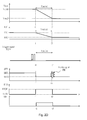
- FIG. 2B shows a schematic diagram of signal waveforms according to an embodiment of the present invention.
- the control circuit 205 may receive the setting signal SET from an external circuit, or alternatively, generate the setting signal SET internally according to the programmable output voltage Vout or its related signal, the input current Iin or its related signal, or an output current Iout or its related signal.
- FIG. 2B shows an example that the control circuit 205 receives the setting signal SET from an external circuit.
- the setting signal SET may be provided externally, for example may come from a load circuit (not shown) coupled to the output node OUT, or by a user's direct setting.
- FIG. 2B shows one possible signal waveform of the setting signal SET.
- the target of the programmable output voltage Vout is the predetermined level Vout 1 ; and after the setting signal SET changes from the level SET 1 to a level SET 2 at time point t 1 , the target of the programmable output voltage Vout changes from the predetermined level Vout 1 to the predetermined level Vout 2 .
- the control circuit 205 adjusts the operation signal GATE according to a change of the setting signal SET from the level SET 1 to the level SET 2 , to control the power switch of the power switch circuit 103 , such that the programmable output voltage Vout switches form the predetermined level Vout 1 to the predetermined level Vout 2 .
- the output capacitor C 1 is electrically connected between the output node OUT and the reference level REF, the output capacitor C 1 needs to be discharged when the programmable output voltage Vout changes from the predetermined level Vout 1 to the predetermined level Vout 2 . Therefore, a transition period is required to discharge the output capacitor C 1 when the programmable output voltage Vout changes from the predetermined level Vout 1 to the predetermined level Vout 2 .
- a transition period Tperiod is required for the programmable output voltage Vout to drop from the predetermined level Vout 1 to the predetermined level Vout 2 , and the programmable output voltage Vout reaches the predetermined level Vout 2 at a time point t 2 .
- the control circuit 205 adjusts the bleeding signal BLD according to the change of the setting signal SET. For example, the control circuit 205 adjusts the bleeding signal BLD from a low level LOW to a high level HIGH when the setting signal SET changes from the level SET 1 to the level SET 2 , for a period of time (discharge time period).
- This discharge time period that the bleeding signal BLD is at the high level HIGH for example can be but is not limited to the transition period Tperiod (from the time point t 1 to the time point t 2 ); for another example, the discharge time period can be a period shorter than the transition period Tperiod.
- the discharge current Id flows through the discharge circuit 208 to discharge the output capacitor C 1 , such that the transition period Tperiod for the programmable output voltage Vout to drop from the predetermined level Vout 1 to the predetermined level Vout 2 is shortened.
- the feedback signal FB also changes from a level FB 1 to a level FB 2 .
- the present invention is applied to a power supply circuit having an isolated structure. That is, the circuits at the same side of the primary winding W 1 of the transformer circuit 102 , including the control circuit 205 , the power switch circuit 103 , the input current sense circuit 106 , and the output voltage sense circuit 107 etc., have a relative low level which is the ground level GND; and the circuits at the same side of the secondary winding W 2 of the transformer circuit 102 , including the output capacitor C 1 and the discharge circuit 208 etc., have a relative low level which is the reference level REF, wherein the ground level GND is isolated from the reference level REF, as well known by those skilled in the art.
- FIG. 3 shows a second embodiment of an isolated power supply circuit 300 with the programmable function of the present invention.
- This embodiment shows a more specific embodiment of a discharge circuit 308 according to the present invention.
- a control circuit 305 adjusts the operation signal GATE according to the setting signal SET, to switch the programmable output voltage Vout between different predetermined levels at the output node OUT.
- the control circuit 305 determines the bleeding signal BLD to adjust the discharging current Idis to discharge the output capacitor C 1 when the programmable output voltage Vout switches between different predetermined levels.
- the discharge circuit 308 for example includes an opto-coupler 3081 and a voltage difference circuit 3082 , wherein the opto-coupler 3081 is controlled by the bleeding signal BLD to generate a current between the output node OUT and the reference level REF, which is the discharging current Idis.
- the voltage difference circuit 3082 includes for example but not limited to a resistor as shown in the figure, which is coupled to the opto-coupler 3081 and the output node OUT, for providing a voltage drop in the current path of the discharging current Idis.
- the discharging current Idis discharges the output capacitor C 1 so as to shorten the transition period Tperiod.
- FIG. 4 shows a third embodiment of an isolated power supply circuit 400 with the programmable function according to the present invention.
- This embodiment shows a more specific embodiment of a discharge circuit 408 according to the present invention.
- the discharge circuit 408 includes the opto-coupler 3081 and a voltage difference circuit 4082 , wherein the phot-coupler 3081 is coupled to a control circuit 405 , for generating the discharging current Idis according to the bleeding signal BLD, and the voltage difference circuit 4082 includes for example but not limited to a transistor Q 1 , which is coupled to the opto-coupler 3081 and the output node OUT, for providing a voltage drop in the current path of the discharging current Idis.
- the transistor Q 1 is for example but not limited to a metal oxide semiconductor (MOS) device or a bipolar junction transistor (BJT) device.
- the control circuit 405 adjusts the operation signal GATE according to the setting signal SET, to switch the programmable output voltage Vout between different predetermined levels at the output node OUT, for example from the higher predetermined level Vout 1 to the lower predetermined level Vout 2 .
- the control circuit 405 determines the bleeding signal BLD, which controls the discharging current Idis to discharge the output capacitor C 1 when the programmable output voltage switches between different predetermined levels in the transition period Tperiod.
- the figure shows that, instead of providing the setting signal SET from an external circuit which is one possible embodiment, the setting signal SET may be adjusted or determined according to the programmable output voltage Vout or its related signal, the input current Iin or its related signal, or the output current Iout or its related signal, or a combination of two or more of the above.
- FIG. 2C shows a schematic diagram of the signal waveforms of another embodiment according to the present invention.
- the control circuit 405 may adjust the setting signal SET according to the programmable output voltage Vout or its related signal, the input current Iin or its related signal, or the output current Iout or its related signal, wherein the programmable output voltage Vout or its related signal, the input current Iin or its related signal, or the output current Iout or its related signal includes a trigger signal TG.
- the feedback signal FB which is a signal related to the programmable output voltage Vout.
- the trigger signal TG triggers the discharging current Idis to start discharging the output capacitor C 1 .
- the feedback signal FB includes the trigger signal TG, wherein the trigger signal TG may be added to the feedback signal FB for example by a communication protocol.
- the communication protocol for example is used for the communication between the load circuit and the control circuit 405 , and a code may be predefined in the communication protocol which instructs to generate the trigger signal TG.
- the communication protocol between the load circuit and the control circuit 405 can be defined in any way.
- the trigger signal TG is inputted to the control circuit 405 before the time point t 1 , and the control circuit 405 changes the setting signal SET from the level SET 1 to the level SET 2 according to the trigger signal TG in the feedback signal FB, indicating that the target of the programmable output voltage Vout is switched to the predetermined level Vout 2 . Accordingly, the control circuit 405 adjusts the operation signal GATE, to control the power switch of the power switch circuit 103 such that the programmable output voltage Vout is changed from the predetermined level Vout 1 to the predetermined level Vout 2 .
- a transition period Tperiod is required for the programmable output voltage Vout to drop from the predetermined level Vout 1 to the predetermined level Vout 2 , and the programmable output voltage Vout reaches the predetermined level Vout 2 at a time point t 3 .
- the control circuit 405 adjusts the bleeding signal BLD according to the change of the setting signal SET.
- the bleeding signal BLD is changed from a low level LOW to a high level HIGH for a period of time (discharge time period).
- This discharge time period for example can be but is not limited to the transition period Tperiod (from the time point t 1 to the time point t 3 ); for another example, the discharge time period can be a period shorter than the transition period Tperiod.
- the discharge current Id flows through the discharge circuit 408 to discharge the output capacitor C 1 , such that the transition period Tperiod for the programmable output voltage Vout to switch from the predetermined level Vout 1 to the predetermined level Vout 2 is shortened.
- the trigger signal TG is for example a square wave signal added to the feedback signal FB.
- the present invention can be embodied in other ways.
- the trigger signal TG may be in other forms, or may be a digital or analog signal separated from the setting signal SET.
- control circuit 405 may further adjust the setting signal SET according to the programmable output voltage Vout or its related signal, to provide a finish signal FH.
- a single pulse signal is added to the setting signal SET at the time point t 3 .
- the finish signal FH indicates to stop discharging the output capacitor C 1 by the discharging signal Idis.
- the finish signal FH is related to the predetermined level Vout 2 , and it may be generated for example as thus: when the programmable output voltage Vout decreases to the predetermined level Vout 2 , the feedback signal FB (which is a signal related to the programmable output voltage Vout) changes to the level FB 2 , and the control circuit 405 adjusts the setting signal SET according to the feedback signal FB.
- the setting signal SET, the trigger signal TG and the finish signal FH are not limited to the waveforms as shown in the figure, but may be in other forms such as a group of pulses, or other forms of digital or analog signals.
- control circuit 405 may adjust the setting signal SET to generate a single pulse at the time point t 3 , or to change a level of the setting signal SET at the time point t 3 .
- control circuit 405 may generate another signal separated from the setting signal SET (form another perspective, this other signal and the original setting signal SET can be regarded as one setting signal SET having two parallel parts transmitted by two parallel lines).
- the aforementioned adjustment of the setting signal SET indicates that the bleeding signal BLD should be adjusted, to start the discharging current according to the trigger signal TG and to decrease the discharging current preferably zero current according to the finish signal FH.
- FIG. 2D shows a schematic diagram of the signal waveforms of another embodiment according to the present invention.
- the control circuit 405 may adjust the setting signal SET according to the programmable output voltage Vout or its related signal, the input current Iin or its related signal, or the output current Iout or its related signal, wherein the programmable output voltage Vout or its related signal, the input current Iin or its related signal, or the output current Iout or its related signal includes a trigger signal TG′.
- the feedback signal FB which is a signal related to the programmable output voltage Vout.
- the trigger signal TG′ triggers the discharging current Idis to start discharging the output capacitor C 1 .
- the setting signal SET is determined by for example but not limited to the control circuit 405 according to the feedback signal FB.
- the feedback signal FB includes the trigger signal TG′ and a signal FB′ which are two separate signals, wherein the trigger signal TG′ may be generated by a communication protocol.
- the communication protocol for example is used for the communication between the load circuit and the control circuit 405 , and a code may be predefined in the communication protocol which instructs to generate the trigger signal TG′ with the signal FB′.
- the communication protocol between the load circuit and the control circuit 405 can be defined in any way.
- the trigger signal TG′ is inputted to the control circuit 405 before the time point t 1 , and the control circuit 405 changes the setting signal SET from the level SET 1 to the level Set 2 according to the trigger signal TG′ in the feedback signal FB, indicating that the target of the programmable output voltage Vout is switched to the predetermined level Vout 2 . Accordingly, the control circuit 405 adjusts the operation signal GATE, to control the power switch of the power switch circuit 103 such that the programmable output voltage Vout is changed from the predetermined level Vout 1 to the predetermined level Vout 2 .
- a transition period Tperiod is required for the programmable output voltage Vout to drop from the predetermined level Vout 1 to the predetermined level Vout 2 , and the programmable output voltage Vout reaches the predetermined level Vout 2 at a time point t 3 .
- the control circuit 405 adjusts the bleeding signal BLD according to the change of the setting signal SET.
- the bleeding signal BLD is changed from a low level LOW to a high level HIGH for a period of time (discharge time period).
- This discharge time period for example can be but is not limited to the transition period Tperiod (from the time point t 1 to the time point t 3 ); for another example, the discharge time period can be a period shorter than the transition period Tperiod.
- the discharge current Id flows through the discharge circuit 408 to discharge the output capacitor C 1 , such that the transition period Tperiod for the programmable output voltage Vout to switch from the predetermined level Vout 1 to the predetermined level Vout 2 is shortened.
- the trigger signal TG′ and the signal FB′ are two separate signals which can be regarded as one feedback signal FB having two parallel parts transmitted by two parallel lines.
- the present invention can be embodied in other ways.
- the trigger signal TG′ may be grouped with other signals, such as the programmable signal Vout or its related signal, the input current Iin or its related signal, or the output current Iout or its related signal, to be inputted to the control circuit 405 .
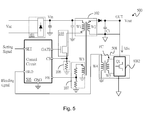
- FIG. 5 shows a fourth embodiment of the present invention, which is another embodiment of the isolated power supply circuit 500 with the programmable function.
- the output voltage sense circuit 107 and the discharge circuit 508 may respectively include transformer circuits to generate the feedback signal FB and the discharging current Idis.
- the discharge circuit 508 includes a transformer circuit and a voltage difference circuit 4082 .
- the transformer circuit includes a discharger primary winding W 4 and a discharger secondary winding W 5 .
- the discharger primary winding W 4 is coupled to the control circuit 505 , for receiving the bleeding signal BLD.
- the discharger secondary winding W 5 is coupled to the discharger primary winding W 4 , and the discharger secondary winding W 5 senses the bleeding signal BLD through the discharger primary winding W 4 to generate a coupled signal.
- the voltage difference circuit 4082 for example includes a transistor Q 1 , and it is coupled to the discharge secondary winding W 5 and the output node OUT, for generating the discharging current Idis according to the coupled signal.
- the voltage difference circuit 4082 for example is connected to the discharge secondary winding W 5 in parallel.
- the control circuit 505 adjusts the operation signal GATE according to the setting signal SET, to switch the programmable output voltage Vout between different predetermined levels at the output node OUT.
- the control circuit 505 determines the bleeding signal BLD which controls the discharging current Idis to discharge the output capacitor C 1 when the programmable output voltage Vout switches between different predetermined levels (for example, dropping from a higher level to a lower level).
- the present invention has been described in considerable detail with reference to certain preferred embodiments thereof. It should be understood that the description is for illustrative purpose, not for limiting the scope of the present invention. Those skilled in this art can readily conceive variations and modifications within the spirit of the present invention.
- a device or circuit which does not substantially influence the primary function of a signal can be inserted between any two devices or circuits in the shown embodiments, so the term “couple” should include direct and indirect connections.
- the resistors or the divider circuit is not limited to a circuit formed by passive devices, but it may be other circuits, such as a transistor circuit.
- the discharging current Idis is not limited to having a fixed level as show in the figures, but may have any waveform.
- the programmable output voltage Vout or its related signal, the input current Iin and its related signal, or the output current Iout or its related signal shown in the embodiments of the present invention is not limited to the feedback signal FB, but can be any other signal of the above-mentioned categories, such as the current sense signal CS, etc.
- the trigger signal TG is not limited to the square signal as shown in the figures, but may be a signal of any waveform.
- the programmable output voltage Vout is not limited to having two different predetermined levels Vout 1 and Vout 2 , but may have three or more different predetermined levels.
- the setting signal is not limited to the square signal as shown in the figures, but may be a signal of any other waveform, or a signal of another form such as a digital signal, or a signal including plural sub-signals.
- the spirit of the present invention should cover all such and other modifications and variations, which should be interpreted to fall within the scope of the following claims and their equivalents.
Landscapes
- Engineering & Computer Science (AREA)
- Power Engineering (AREA)
- Dc-Dc Converters (AREA)
Abstract
Description
- The present invention claims priority to U.S. 61/975,296, filed on Apr. 4, 2014.
- 1. Field of Invention
- The present invention relates to an isolated power supply circuit with a programmable function and a control method thereof; particularly, it relates to such isolated power supply circuit and control method thereof with a relatively shorter output level transition period.
- 2. Description of Related Art
-
FIG. 1 shows a schematic diagram of a conventional isolatedpower supply circuit 100. As shown inFIG. 1 , arectifier circuit 101 rectifies an AC voltage Vac to generate an input voltage Vin. Therectifier circuit 101 is for example a bridge rectifier circuit. Atransformer circuit 102 of the isolatedpower supply circuit 100 receives the input voltage Vin, and converts it to an output voltage Vo. The isolatedpower supply circuit 100 includes theaforementioned transformer circuit 102, apower switch circuit 103, acontrol circuit 105, an inputcurrent sense circuit 106, and an outputvoltage sense circuit 107. Thecontrol circuit 105 generates an operation signal GATE according to a current sense signal CS generated by the inputcurrent sense circuit 106 and a feedback signal FB generated by the outputvoltage sense circuit 107, for converting the input voltage Vin to the output voltage Vo. Thetransformer circuit 102 includes a primary winding W1 and a secondary winding W2. The secondary winding w2 is electrically connected to a reference level REF, and the primary winding W1 and a third winding W3 are coupled to a ground level GND. The outputvoltage sense circuit 107 senses the output voltage Vo by the third winding W3 to generate the feedback signal FB, wherein voltage across the third winding W3 is proportional to the voltage across the secondary winding W2, i.e., the output voltage Vo. For better logic in description, the third winding W3 is described as a part of the outputvoltage sense circuit 107; in circuit implementation, the third winding W3 may be included as a part of thetransformer circuit 102. - The aforementioned conventional isolated
power supply circuit 100 can only provide the output voltage Vo at one single predetermined level. The conventional isolatedpower supply circuit 100 can not provide different output voltages Vo at different levels according to different loading requirements. There is another prior art isolated power supply circuit which provides a programmable function wherein the output voltage Vo can switch between different levels, but this prior art requires a long transition period when the output voltage Vo switches from one level to another. - In view of the above, the present invention proposes an isolated power supply circuit with a programmable function and a control method thereof, whereby a transition period between different output voltage levels is shortened.
- From one perspective, the present invention provides an isolated power supply circuit with a programmable function; the isolated power supply circuit with a programmable function includes: a first transformer circuit, which includes a primary winding and a secondary winding, wherein the primary winding receives an input voltage and the secondary winding generates a programmable output voltage at an output node; a power switch circuit, which is coupled to the primary winding, the power switch circuit operating according to an operation signal to convert the input voltage to the programmable output voltage; a discharge circuit, which is coupled to the output node, for generating a discharging current according to a bleeding signal; and a control circuit, which is coupled to the power switch circuit and the discharge circuit, for generating the operation signal and the bleeding signal at least according to a setting signal; wherein the control circuit adjusts the operation signal according to the setting signal, such that the programmable output voltage switches from a first predetermined level to a second predetermined level, and in a transition period when the programmable output voltage switches from the first predetermined level to the second predetermined level, the control circuit determines the bleeding signal whereby the discharge circuit adjusts the discharging current, so that the discharging current discharges the programmable output voltage.
- In one preferable embodiment, the isolated power supply circuit further includes an output voltage sense circuit, which is coupled between the transformer circuit and the control circuit, for generating a feedback signal according to the programmable output voltage.
- In one preferable embodiment, the output voltage sense circuit includes: a tertiary winding, which is coupled to the secondary winding, for generating a sense signal according to the programmable output voltage; and a conversion circuit, which is coupled to the tertiary winding, for converting the sense signal to the feedback signal.
- In one preferable embodiment, the control circuit adjusts the setting signal according to the programmable output voltage or a signal related to the programmable output voltage, an input current or a signal related to the input current, or an output current or a signal related to the output current, wherein the programmable output voltage or the signal related to the programmable output voltage, the input current or the signal related to the input current, or the output current or the signal related to the output current includes a trigger signal which triggers the discharging current to discharge the programmable output voltage.
- In one preferable embodiment, the setting signal includes a finish signal indicating to stop discharging the programmable output voltage.
- In one preferable embodiment, the discharge circuit includes: an opto-coupler, which is coupled to the control circuit, for generating the discharge current according to the bleeding signal; and a voltage difference circuit, which is coupled to the opto-coupler, for providing a voltage difference in a path of the discharging current.
- In one preferable embodiment, the discharge circuit includes: a second transformer circuit, which has: a discharger primary winding, which is coupled to the control circuit, for receiving the bleeding signal; and a discharger secondary winding, which is coupled to the discharger primary winding, for sensing the bleeding signal to generate a coupled signal; and a voltage difference circuit, which is coupled to the discharge secondary winding and the output node, for generating the discharging current according to the coupled signal.
- In one preferable embodiment, the isolated power supply circuit further includes an input current sense circuit, which is coupled to the power switch circuit and the control circuit, for generating a current sense signal according to an input current flowing through the power switch circuit, such that the control circuit generates the operation signal further according to the current sense signal.
- From another perspective, the present invention provides a control method of an isolated power supply circuit with a programmable function, wherein the isolated power supply circuit includes a first transformer circuit, which has a primary winding and a secondary winding, the control method including: receiving an input voltage by the primary winding and generating a programmable output voltage at an output node by the secondary winding; operating a power switch circuit according to an operation signal to convert the input voltage to the programmable output voltage, wherein the power switch circuit is coupled to the primary winding; adjusting the operation signal according to a setting signal, such that the programmable output voltage switches from a first predetermined level to a second predetermined level; generating a bleeding signal according to the setting signal in a transition period when the programmable output voltage switches from the first predetermined level to the second predetermined level; and generating a discharging current according to the bleeding signal, whereby the discharging current discharges the programmable output voltage in the transition period.
- In one preferable embodiment, the control method further includes: generating a feedback signal according to the programmable output voltage.
- In one preferable embodiment, the step of generating the feedback signal according to the programmable output voltage includes: generating a sense signal by sensing the programmable output voltage with a tertiary winding which is coupled to the secondary winding; and converting the sense signal to the feedback signal.
- In one preferable embodiment, the control method further includes: adjusting the setting signal according to the programmable output voltage or a signal related to the programmable output voltage, an input current or a signal related to the input current, or an output current or a signal related to the output current, wherein the programmable output voltage or the signal related to the programmable output voltage, the input current or the signal related to the input current, or the output current or the signal related to the output current includes a trigger signal which triggers the discharging current to discharge the programmable output voltage.
- In one preferable embodiment, the setting signal includes a finish signal indicating to stop discharging the programmable output voltage.
- In one preferable embodiment, the step of generating the discharging current according to the bleeding signal includes: transmitting the bleeding signal through opto-coupling to generate the discharging current.
- In one preferable embodiment, the step of generating a discharging current according to the bleeding signal includes: receiving the bleeding signal by a discharger primary winding; sensing the bleeding signal to generate a coupled signal by a secondary winding; and generating the discharging current according to the coupled signal.
- In one preferable embodiment, the control method further includes: generating a current sense signal according to an input current flowing through the power switch circuit, such that the operation signal is adjusted further according to the current sense signal.
- The objectives, technical details, features, and effects of the present invention will be better understood with regard to the detailed description of the embodiments below.
-
FIG. 1 shows a schematic diagram of a conventional isolatedpower supply circuit 100. -
FIG. 2A shows a first embodiment of the present invention. -
FIGS. 2B-2D show schematic diagrams of signal waveforms according to several embodiments of the present invention. -
FIG. 3 shows a second embodiment of the present invention. -
FIG. 4 shows a third embodiment of the present invention. -
FIG. 5 shows a fourth embodiment of the present invention. - Please refer to
FIG. 2A for a first embodiment according to the present invention. As shown inFIG. 2A , an isolatedpower supply circuit 200 with a programmable function includes atransformer circuit 102, apower switch circuit 103, acontrol circuit 205, an inputcurrent sense circuit 106, an outputvoltage sense circuit 107, and adischarge circuit 208. Thetransformer circuit 102 includes a primary winding W1 and a secondary winding W2. Therectifier circuit 101 rectifies an alternating current (AC) voltage Vac to generate an input voltage Vin. Therectifier circuit 101 is well known by those skilled in the art, so details thereof are omitted here. The primary winding W1 receives the input voltage Vin, and the secondary winding W2 generates an output voltage Vout at an output node OUT. Thepower switch circuit 103 is coupled to the primary winding W1, and it operates according to an operation signal GATE to convert the input voltage Vin to a programmable output voltage Vout. Thecontrol circuit 205 generates the operation signal GATE to control thepower switch circuit 103, and thecontrol circuit 205 further generates a bleeding signal BLD to control thedischarge circuit 208. The operation signal GATE is generated according to a setting signal SET, in additional to the current sense signal CS and the feedback signal FB. Thedischarge circuit 208 is coupled to the output node OUT, and thedischarge circuit 208 is controlled by the bleeding signal BLD to generate a discharging current Idis. In this invention, the output voltage Vout is programmable according to the setting signal SET. That is, thecontrol circuit 205 adjusts the operation signal GATE according to the setting signal SET, such that the programmable output voltage Vout switches between different predetermined levels at the output node OUT, for example from a predetermined level 12V to a predetermined level 5V. Ina transition period Tperiod when the programmable output voltage Vout switches from one predetermined level to another predetermined level, thecontrol circuit 205 determines the bleeding signal BLD, whereby thedischarge circuit 208 adjusts the discharging current Idis to discharge an output capacitor C1. The output capacitor C1 is coupled to the output node OUT, and the voltage across the output capacitor C1 corresponds to the programmable output voltage Vout. The inputcurrent sense circuit 106 is coupled to thepower switch circuit 103 and thecontrol circuit 205, for generating a current sense signal CS according to an input current Iin flowing through the power switch. The outputvoltage sense circuit 107 is coupled between thetransformer circuit 102 and thecontrol circuit 205, for generating a feedback signal FB according to the programmable output voltage Vout. The feedback signal FB is related to a level of the programmable output voltage Vout, and the feedback signal for example can be obtained from the programmable output voltage Vout, or as shown in the figure, obtained from a voltage across a tertiary winding W3 which is proportional to a voltage across the secondary winding W2, i.e., the programmable output voltage Vout. Thecontrol circuit 205 generates the operation signal GATE according to the setting signal SET, the current sense signal CS and the feedback signal FB. - According to the present invention, in the first embodiment, the output
voltage sense circuit 107 for example includes the tertiary winding W3 and aconversion circuit 1071. The tertiary winding W3 is coupled to the secondary winding W2, for sensing the programmable output voltage Vout to generate a sense signal. For example, as shown inFIG. 2A , the sense signal is generated at one end of the tertiary winding W3 (which is opposite to the other end electrically connecting to the ground level GND). Theconversion circuit 1071 is electrically connected to the tertiary winding W3 to receive the sense signal. Theconversion circuit 1071 includes for example but not limited to two resistors connected in series, and the feedback signal FB is obtained from a divided voltage across one of the resistors. - The input
current sense circuit 106 includes for example but not limited to a resistor as shown inFIG. 2A , which has one end electrically connected to the ground level GND, and the other end electrically connected to both thepower switch circuit 103 and thecontrol circuit 205. The current sense signal CS inputted to thecontrol circuit 205 may be obtained from a voltage across the resistor of the inputcurrent sense circuit 106 where the aforementioned input current Iin flows through. -
FIG. 2B shows a schematic diagram of signal waveforms according to an embodiment of the present invention. For example, thecontrol circuit 205 may receive the setting signal SET from an external circuit, or alternatively, generate the setting signal SET internally according to the programmable output voltage Vout or its related signal, the input current Iin or its related signal, or an output current Iout or its related signal.FIG. 2B shows an example that thecontrol circuit 205 receives the setting signal SET from an external circuit. The setting signal SET may be provided externally, for example may come from a load circuit (not shown) coupled to the output node OUT, or by a user's direct setting.FIG. 2B shows one possible signal waveform of the setting signal SET. For example, as shown in the figure, when the setting signal SET is at a level SET1 before a time point t1, the target of the programmable output voltage Vout is the predetermined level Vout1; and after the setting signal SET changes from the level SET1 to a level SET2 at time point t1, the target of the programmable output voltage Vout changes from the predetermined level Vout1 to the predetermined level Vout2. Thecontrol circuit 205 adjusts the operation signal GATE according to a change of the setting signal SET from the level SET1 to the level SET2, to control the power switch of thepower switch circuit 103, such that the programmable output voltage Vout switches form the predetermined level Vout1 to the predetermined level Vout2. Because the output capacitor C1 is electrically connected between the output node OUT and the reference level REF, the output capacitor C1 needs to be discharged when the programmable output voltage Vout changes from the predetermined level Vout1 to the predetermined level Vout2. Therefore, a transition period is required to discharge the output capacitor C1 when the programmable output voltage Vout changes from the predetermined level Vout1 to the predetermined level Vout2. As shown in the figure, a transition period Tperiod is required for the programmable output voltage Vout to drop from the predetermined level Vout1 to the predetermined level Vout2, and the programmable output voltage Vout reaches the predetermined level Vout2 at a time point t2. - According to the present invention, in the first embodiment, when the setting signal SET changes from the level SET1 to the level SET2, the
control circuit 205 adjusts the bleeding signal BLD according to the change of the setting signal SET. For example, thecontrol circuit 205 adjusts the bleeding signal BLD from a low level LOW to a high level HIGH when the setting signal SET changes from the level SET1 to the level SET2, for a period of time (discharge time period). This discharge time period that the bleeding signal BLD is at the high level HIGH for example can be but is not limited to the transition period Tperiod (from the time point t1 to the time point t2); for another example, the discharge time period can be a period shorter than the transition period Tperiod. In the discharge time period, the discharge current Idis flows through thedischarge circuit 208 to discharge the output capacitor C1, such that the transition period Tperiod for the programmable output voltage Vout to drop from the predetermined level Vout1 to the predetermined level Vout2 is shortened. When the programmable output voltage Vout changes from the predetermined level Vout1 to the predetermined level Vout2, the feedback signal FB also changes from a level FB1 to a level FB2. - Note that the present invention is applied to a power supply circuit having an isolated structure. That is, the circuits at the same side of the primary winding W1 of the
transformer circuit 102, including thecontrol circuit 205, thepower switch circuit 103, the inputcurrent sense circuit 106, and the outputvoltage sense circuit 107 etc., have a relative low level which is the ground level GND; and the circuits at the same side of the secondary winding W2 of thetransformer circuit 102, including the output capacitor C1 and thedischarge circuit 208 etc., have a relative low level which is the reference level REF, wherein the ground level GND is isolated from the reference level REF, as well known by those skilled in the art. -
FIG. 3 shows a second embodiment of an isolatedpower supply circuit 300 with the programmable function of the present invention. This embodiment shows a more specific embodiment of adischarge circuit 308 according to the present invention. As shown inFIG. 3 , in this embodiment, acontrol circuit 305 adjusts the operation signal GATE according to the setting signal SET, to switch the programmable output voltage Vout between different predetermined levels at the output node OUT. Thecontrol circuit 305 determines the bleeding signal BLD to adjust the discharging current Idis to discharge the output capacitor C1 when the programmable output voltage Vout switches between different predetermined levels. Thedischarge circuit 308 for example includes an opto-coupler 3081 and avoltage difference circuit 3082, wherein the opto-coupler 3081 is controlled by the bleeding signal BLD to generate a current between the output node OUT and the reference level REF, which is the discharging current Idis. Thevoltage difference circuit 3082 includes for example but not limited to a resistor as shown in the figure, which is coupled to the opto-coupler 3081 and the output node OUT, for providing a voltage drop in the current path of the discharging current Idis. The discharging current Idis discharges the output capacitor C1 so as to shorten the transition period Tperiod. -
FIG. 4 shows a third embodiment of an isolatedpower supply circuit 400 with the programmable function according to the present invention. This embodiment shows a more specific embodiment of adischarge circuit 408 according to the present invention. As shown inFIG. 4 , in this embodiment, thedischarge circuit 408 includes the opto-coupler 3081 and avoltage difference circuit 4082, wherein the phot-coupler 3081 is coupled to acontrol circuit 405, for generating the discharging current Idis according to the bleeding signal BLD, and thevoltage difference circuit 4082 includes for example but not limited to a transistor Q1, which is coupled to the opto-coupler 3081 and the output node OUT, for providing a voltage drop in the current path of the discharging current Idis. The transistor Q1 is for example but not limited to a metal oxide semiconductor (MOS) device or a bipolar junction transistor (BJT) device. Thecontrol circuit 405 adjusts the operation signal GATE according to the setting signal SET, to switch the programmable output voltage Vout between different predetermined levels at the output node OUT, for example from the higher predetermined level Vout1 to the lower predetermined level Vout2. Thecontrol circuit 405 determines the bleeding signal BLD, which controls the discharging current Idis to discharge the output capacitor C1 when the programmable output voltage switches between different predetermined levels in the transition period Tperiod. - Note that in this embodiment, the figure shows that, instead of providing the setting signal SET from an external circuit which is one possible embodiment, the setting signal SET may be adjusted or determined according to the programmable output voltage Vout or its related signal, the input current Iin or its related signal, or the output current Iout or its related signal, or a combination of two or more of the above.
- Please refer to
FIG. 2C , which shows a schematic diagram of the signal waveforms of another embodiment according to the present invention. Please also refer toFIG. 4 . Thecontrol circuit 405 may adjust the setting signal SET according to the programmable output voltage Vout or its related signal, the input current Iin or its related signal, or the output current Iout or its related signal, wherein the programmable output voltage Vout or its related signal, the input current Iin or its related signal, or the output current Iout or its related signal includes a trigger signal TG. (InFIG. 2C , an example is given by the feedback signal FB, which is a signal related to the programmable output voltage Vout.) The trigger signal TG triggers the discharging current Idis to start discharging the output capacitor C1. As shown inFIG. 2C , the feedback signal FB includes the trigger signal TG, wherein the trigger signal TG may be added to the feedback signal FB for example by a communication protocol. The communication protocol for example is used for the communication between the load circuit and thecontrol circuit 405, and a code may be predefined in the communication protocol which instructs to generate the trigger signal TG. The communication protocol between the load circuit and thecontrol circuit 405 can be defined in any way. - The trigger signal TG is inputted to the
control circuit 405 before the time point t1, and thecontrol circuit 405 changes the setting signal SET from the level SET1 to the level SET2 according to the trigger signal TG in the feedback signal FB, indicating that the target of the programmable output voltage Vout is switched to the predetermined level Vout2. Accordingly, thecontrol circuit 405 adjusts the operation signal GATE, to control the power switch of thepower switch circuit 103 such that the programmable output voltage Vout is changed from the predetermined level Vout1 to the predetermined level Vout2. As shown in the figure, a transition period Tperiod is required for the programmable output voltage Vout to drop from the predetermined level Vout1 to the predetermined level Vout2, and the programmable output voltage Vout reaches the predetermined level Vout2 at a time point t3. - According to the present invention, in this embodiment, when the setting signal SET changes from the level SET1 to the level SET2, the
control circuit 405 adjusts the bleeding signal BLD according to the change of the setting signal SET. For example, when or after the setting signal SET changes from the level SET1 to the level SET2, the bleeding signal BLD is changed from a low level LOW to a high level HIGH for a period of time (discharge time period). This discharge time period for example can be but is not limited to the transition period Tperiod (from the time point t1 to the time point t3); for another example, the discharge time period can be a period shorter than the transition period Tperiod. In the discharge time period, the discharge current Idis flows through thedischarge circuit 408 to discharge the output capacitor C1, such that the transition period Tperiod for the programmable output voltage Vout to switch from the predetermined level Vout1 to the predetermined level Vout2 is shortened. In the shown embodiment, the trigger signal TG is for example a square wave signal added to the feedback signal FB. However, the present invention can be embodied in other ways. For example, the trigger signal TG may be in other forms, or may be a digital or analog signal separated from the setting signal SET. - Still referring to
FIG. 2C , thecontrol circuit 405 may further adjust the setting signal SET according to the programmable output voltage Vout or its related signal, to provide a finish signal FH. For example, as shown in the figure, a single pulse signal is added to the setting signal SET at the time point t3. The finish signal FH indicates to stop discharging the output capacitor C1 by the discharging signal Idis. The finish signal FH is related to the predetermined level Vout2, and it may be generated for example as thus: when the programmable output voltage Vout decreases to the predetermined level Vout2, the feedback signal FB (which is a signal related to the programmable output voltage Vout) changes to the level FB2, and thecontrol circuit 405 adjusts the setting signal SET according to the feedback signal FB. The setting signal SET, the trigger signal TG and the finish signal FH are not limited to the waveforms as shown in the figure, but may be in other forms such as a group of pulses, or other forms of digital or analog signals. For example, thecontrol circuit 405 may adjust the setting signal SET to generate a single pulse at the time point t3, or to change a level of the setting signal SET at the time point t3. Or, thecontrol circuit 405 may generate another signal separated from the setting signal SET (form another perspective, this other signal and the original setting signal SET can be regarded as one setting signal SET having two parallel parts transmitted by two parallel lines). The aforementioned adjustment of the setting signal SET indicates that the bleeding signal BLD should be adjusted, to start the discharging current according to the trigger signal TG and to decrease the discharging current preferably zero current according to the finish signal FH. - Please refer to
FIG. 2D , which shows a schematic diagram of the signal waveforms of another embodiment according to the present invention. Please also refer toFIG. 4 . Thecontrol circuit 405 may adjust the setting signal SET according to the programmable output voltage Vout or its related signal, the input current Iin or its related signal, or the output current Iout or its related signal, wherein the programmable output voltage Vout or its related signal, the input current Iin or its related signal, or the output current Iout or its related signal includes a trigger signal TG′. (InFIG. 2D , an example is given by the feedback signal FB, which is a signal related to the programmable output voltage Vout.) The trigger signal TG′ triggers the discharging current Idis to start discharging the output capacitor C1. The setting signal SET is determined by for example but not limited to thecontrol circuit 405 according to the feedback signal FB. As shown inFIG. 2D , the feedback signal FB includes the trigger signal TG′ and a signal FB′ which are two separate signals, wherein the trigger signal TG′ may be generated by a communication protocol. The communication protocol for example is used for the communication between the load circuit and thecontrol circuit 405, and a code may be predefined in the communication protocol which instructs to generate the trigger signal TG′ with the signal FB′. The communication protocol between the load circuit and thecontrol circuit 405 can be defined in any way. - The trigger signal TG′ is inputted to the
control circuit 405 before the time point t1, and thecontrol circuit 405 changes the setting signal SET from the level SET1 to the level Set2 according to the trigger signal TG′ in the feedback signal FB, indicating that the target of the programmable output voltage Vout is switched to the predetermined level Vout2. Accordingly, thecontrol circuit 405 adjusts the operation signal GATE, to control the power switch of thepower switch circuit 103 such that the programmable output voltage Vout is changed from the predetermined level Vout1 to the predetermined level Vout2. As shown in the figure, a transition period Tperiod is required for the programmable output voltage Vout to drop from the predetermined level Vout1 to the predetermined level Vout2, and the programmable output voltage Vout reaches the predetermined level Vout2 at a time point t3. - According to the present invention, in this embodiment, when the setting signal SET changes from the level SET1 to the level SET2, the
control circuit 405 adjusts the bleeding signal BLD according to the change of the setting signal SET. For example, when or after the setting signal SET changes from the level SET1 to the level SET2, the bleeding signal BLD is changed from a low level LOW to a high level HIGH for a period of time (discharge time period). This discharge time period for example can be but is not limited to the transition period Tperiod (from the time point t1 to the time point t3); for another example, the discharge time period can be a period shorter than the transition period Tperiod. In the discharge time period, the discharge current Idis flows through thedischarge circuit 408 to discharge the output capacitor C1, such that the transition period Tperiod for the programmable output voltage Vout to switch from the predetermined level Vout1 to the predetermined level Vout2 is shortened. In the shown embodiment, the trigger signal TG′ and the signal FB′ are two separate signals which can be regarded as one feedback signal FB having two parallel parts transmitted by two parallel lines. However, the present invention can be embodied in other ways. For example, the trigger signal TG′ may be grouped with other signals, such as the programmable signal Vout or its related signal, the input current Iin or its related signal, or the output current Iout or its related signal, to be inputted to thecontrol circuit 405. -
FIG. 5 shows a fourth embodiment of the present invention, which is another embodiment of the isolatedpower supply circuit 500 with the programmable function. This embodiment shows that the outputvoltage sense circuit 107 and thedischarge circuit 508 may respectively include transformer circuits to generate the feedback signal FB and the discharging current Idis. As shown inFIG. 5 , thedischarge circuit 508 includes a transformer circuit and avoltage difference circuit 4082. The transformer circuit includes a discharger primary winding W4 and a discharger secondary winding W5. The discharger primary winding W4 is coupled to thecontrol circuit 505, for receiving the bleeding signal BLD. The discharger secondary winding W5 is coupled to the discharger primary winding W4, and the discharger secondary winding W5 senses the bleeding signal BLD through the discharger primary winding W4 to generate a coupled signal. Thevoltage difference circuit 4082 for example includes a transistor Q1, and it is coupled to the discharge secondary winding W5 and the output node OUT, for generating the discharging current Idis according to the coupled signal. Thevoltage difference circuit 4082 for example is connected to the discharge secondary winding W5 in parallel. Thecontrol circuit 505 adjusts the operation signal GATE according to the setting signal SET, to switch the programmable output voltage Vout between different predetermined levels at the output node OUT. Thecontrol circuit 505 determines the bleeding signal BLD which controls the discharging current Idis to discharge the output capacitor C1 when the programmable output voltage Vout switches between different predetermined levels (for example, dropping from a higher level to a lower level). - The present invention has been described in considerable detail with reference to certain preferred embodiments thereof. It should be understood that the description is for illustrative purpose, not for limiting the scope of the present invention. Those skilled in this art can readily conceive variations and modifications within the spirit of the present invention. For example, a device or circuit which does not substantially influence the primary function of a signal can be inserted between any two devices or circuits in the shown embodiments, so the term “couple” should include direct and indirect connections. For another example, the resistors or the divider circuit is not limited to a circuit formed by passive devices, but it may be other circuits, such as a transistor circuit. For another example, the discharging current Idis is not limited to having a fixed level as show in the figures, but may have any waveform. For another example, the programmable output voltage Vout or its related signal, the input current Iin and its related signal, or the output current Iout or its related signal shown in the embodiments of the present invention is not limited to the feedback signal FB, but can be any other signal of the above-mentioned categories, such as the current sense signal CS, etc. For another example, the trigger signal TG is not limited to the square signal as shown in the figures, but may be a signal of any waveform. For another example, the programmable output voltage Vout is not limited to having two different predetermined levels Vout1 and Vout2, but may have three or more different predetermined levels. For another example, the setting signal is not limited to the square signal as shown in the figures, but may be a signal of any other waveform, or a signal of another form such as a digital signal, or a signal including plural sub-signals. In view of the foregoing, the spirit of the present invention should cover all such and other modifications and variations, which should be interpreted to fall within the scope of the following claims and their equivalents.
Claims (16)
Priority Applications (1)
| Application Number | Priority Date | Filing Date | Title |
|---|---|---|---|
| US14/676,268 US9627984B2 (en) | 2014-04-04 | 2015-04-01 | Isolated power supply circuit with programmable function and control method thereof |
Applications Claiming Priority (2)
| Application Number | Priority Date | Filing Date | Title |
|---|---|---|---|
| US201461975296P | 2014-04-04 | 2014-04-04 | |
| US14/676,268 US9627984B2 (en) | 2014-04-04 | 2015-04-01 | Isolated power supply circuit with programmable function and control method thereof |
Publications (2)
| Publication Number | Publication Date |
|---|---|
| US20150288288A1 true US20150288288A1 (en) | 2015-10-08 |
| US9627984B2 US9627984B2 (en) | 2017-04-18 |
Family
ID=54210625
Family Applications (1)
| Application Number | Title | Priority Date | Filing Date |
|---|---|---|---|
| US14/676,268 Expired - Fee Related US9627984B2 (en) | 2014-04-04 | 2015-04-01 | Isolated power supply circuit with programmable function and control method thereof |
Country Status (3)
| Country | Link |
|---|---|
| US (1) | US9627984B2 (en) |
| CN (1) | CN104980030B (en) |
| TW (1) | TWI538379B (en) |
Cited By (3)
| Publication number | Priority date | Publication date | Assignee | Title |
|---|---|---|---|---|
| US20170207699A1 (en) * | 2016-01-20 | 2017-07-20 | Denso Corporation | Switching power supply device |
| US20180323717A1 (en) * | 2017-05-07 | 2018-11-08 | Richtek Technology Corporation | Flyback power converter circuit and primary side controller circuit and method thereof |
| US20210351707A1 (en) * | 2020-05-06 | 2021-11-11 | Stmicroelectronics S.R.L. | Power supply circuit, corresponding device and method |
Families Citing this family (2)
| Publication number | Priority date | Publication date | Assignee | Title |
|---|---|---|---|---|
| TWI626806B (en) * | 2016-09-20 | 2018-06-11 | 立錡科技股份有限公司 | Charging circuit and capacitive power conversion circuit and charging control method thereof |
| CN113793461B (en) * | 2021-09-16 | 2022-11-04 | 中磊电子(苏州)有限公司 | Video doorbell and automatic setting method thereof |
Citations (16)
| Publication number | Priority date | Publication date | Assignee | Title |
|---|---|---|---|---|
| US20080278973A1 (en) * | 2007-05-11 | 2008-11-13 | Tzu-Chen Lin | Apparatus and method for providing multiple functions and protections for a power converter |
| US20110051463A1 (en) * | 2009-08-14 | 2011-03-03 | Richpower Microelectronics Corporation | Apparatus and method for standby power reduction of a flyback power converter |
| US8106596B2 (en) * | 2008-12-31 | 2012-01-31 | Delta Electronics, Inc. | Light source driving circuit |
| US8111015B2 (en) * | 2008-11-24 | 2012-02-07 | Delta Electronics, Inc. | Brightness-adjustable illumination driving system |
| US20130215651A1 (en) * | 2012-02-18 | 2013-08-22 | Richtek Technology Corporation, R.O.C. | Isolated Power Converter Circuit and Control Method Thereof |
| US20130250627A1 (en) * | 2012-03-20 | 2013-09-26 | Infineon Technologies Austria Ag | Power converter with reduced power consumption in standby mode |
| US8558494B2 (en) * | 2010-11-02 | 2013-10-15 | Delta Electronics, Inc. | Driving device of brushless DC motor for fan |
| US20140019446A1 (en) * | 2008-02-15 | 2014-01-16 | Google Inc. | User interaction based related digital content items |
| US20140139962A1 (en) * | 2012-11-22 | 2014-05-22 | Wago Verwaltungsgesellschaft Mbh | Circuit arrangement having an overload protection for galvanic isolation units |
| US20140192565A1 (en) * | 2013-01-08 | 2014-07-10 | System General Corp. | Circuit with synchronous rectifier for controlling programmable power converter |
| US20140192566A1 (en) * | 2013-01-08 | 2014-07-10 | System General Corporation | Primary-side controlled programmable power converter |
| US20140198535A1 (en) * | 2013-01-15 | 2014-07-17 | System General Corp. | Method and apparatus for controlling programmable power converter with low standby power loss |
| US20140254215A1 (en) * | 2011-08-29 | 2014-09-11 | Power Systems Technologies Ltd. | Controller for a power converter and method of operating the same |
| US20140321167A1 (en) * | 2013-04-24 | 2014-10-30 | Western Digital Technologies, Inc. | Power supply with voltage output responsive to load demand |
| US9190916B2 (en) * | 2012-09-11 | 2015-11-17 | Rohm Co., Ltd. | DC/DC converter, control circuit and control method thereof, power supply, power adapter and electronic apparatus using the same |
| US20160322911A1 (en) * | 2013-12-20 | 2016-11-03 | Byd Company Limited | Integrated circuit that controls switch power supply and switch power supply |
Family Cites Families (7)
| Publication number | Priority date | Publication date | Assignee | Title |
|---|---|---|---|---|
| TWM285132U (en) | 2005-09-05 | 2006-01-01 | Phison Electronics Corp | Switching type power supply unit |
| US20070230222A1 (en) * | 2006-03-31 | 2007-10-04 | Drabing Richard B | Power circuitry for high-frequency applications |
| US7619909B2 (en) * | 2007-12-07 | 2009-11-17 | Leadtrend Technology Corp. | Control circuit for adjusting leading edge blanking time and power converting system using the same control circuit |
| TWI431918B (en) * | 2009-06-19 | 2014-03-21 | Leadtrend Tech Corp | Control method, constant current control method, method for generating a real current source to represent average current through a winding, constant current and constant voltage power converter, switch controller, and average voltage detector |
| TWM385163U (en) | 2010-04-01 | 2010-07-21 | Top Victory Invest Ltd | Output-voltage variable power adapter |
| TWI399022B (en) | 2010-05-24 | 2013-06-11 | Powerforest Technology Corp | A heterodyne dual slope frequency feedback control circuit, control method and the power supply system having the same control circuit |
| CN103199690B (en) * | 2012-01-06 | 2015-06-24 | 西安展芯微电子技术股份有限公司 | X capacitor discharge control device applied to flyback power source |
-
2015
- 2015-03-13 TW TW104108017A patent/TWI538379B/en not_active IP Right Cessation
- 2015-03-19 CN CN201510120666.5A patent/CN104980030B/en not_active Expired - Fee Related
- 2015-04-01 US US14/676,268 patent/US9627984B2/en not_active Expired - Fee Related
Patent Citations (16)
| Publication number | Priority date | Publication date | Assignee | Title |
|---|---|---|---|---|
| US20080278973A1 (en) * | 2007-05-11 | 2008-11-13 | Tzu-Chen Lin | Apparatus and method for providing multiple functions and protections for a power converter |
| US20140019446A1 (en) * | 2008-02-15 | 2014-01-16 | Google Inc. | User interaction based related digital content items |
| US8111015B2 (en) * | 2008-11-24 | 2012-02-07 | Delta Electronics, Inc. | Brightness-adjustable illumination driving system |
| US8106596B2 (en) * | 2008-12-31 | 2012-01-31 | Delta Electronics, Inc. | Light source driving circuit |
| US20110051463A1 (en) * | 2009-08-14 | 2011-03-03 | Richpower Microelectronics Corporation | Apparatus and method for standby power reduction of a flyback power converter |
| US8558494B2 (en) * | 2010-11-02 | 2013-10-15 | Delta Electronics, Inc. | Driving device of brushless DC motor for fan |
| US20140254215A1 (en) * | 2011-08-29 | 2014-09-11 | Power Systems Technologies Ltd. | Controller for a power converter and method of operating the same |
| US20130215651A1 (en) * | 2012-02-18 | 2013-08-22 | Richtek Technology Corporation, R.O.C. | Isolated Power Converter Circuit and Control Method Thereof |
| US20130250627A1 (en) * | 2012-03-20 | 2013-09-26 | Infineon Technologies Austria Ag | Power converter with reduced power consumption in standby mode |
| US9190916B2 (en) * | 2012-09-11 | 2015-11-17 | Rohm Co., Ltd. | DC/DC converter, control circuit and control method thereof, power supply, power adapter and electronic apparatus using the same |
| US20140139962A1 (en) * | 2012-11-22 | 2014-05-22 | Wago Verwaltungsgesellschaft Mbh | Circuit arrangement having an overload protection for galvanic isolation units |
| US20140192565A1 (en) * | 2013-01-08 | 2014-07-10 | System General Corp. | Circuit with synchronous rectifier for controlling programmable power converter |
| US20140192566A1 (en) * | 2013-01-08 | 2014-07-10 | System General Corporation | Primary-side controlled programmable power converter |
| US20140198535A1 (en) * | 2013-01-15 | 2014-07-17 | System General Corp. | Method and apparatus for controlling programmable power converter with low standby power loss |
| US20140321167A1 (en) * | 2013-04-24 | 2014-10-30 | Western Digital Technologies, Inc. | Power supply with voltage output responsive to load demand |
| US20160322911A1 (en) * | 2013-12-20 | 2016-11-03 | Byd Company Limited | Integrated circuit that controls switch power supply and switch power supply |
Cited By (6)
| Publication number | Priority date | Publication date | Assignee | Title |
|---|---|---|---|---|
| US20170207699A1 (en) * | 2016-01-20 | 2017-07-20 | Denso Corporation | Switching power supply device |
| US10468981B2 (en) * | 2016-01-20 | 2019-11-05 | Denso Corporation | Switching power supply device |
| US20180323717A1 (en) * | 2017-05-07 | 2018-11-08 | Richtek Technology Corporation | Flyback power converter circuit and primary side controller circuit and method thereof |
| US10505461B2 (en) * | 2017-05-07 | 2019-12-10 | Richtek Technology Corporation | Flyback power converter circuit and primary side controller circuit and method thereof |
| US20210351707A1 (en) * | 2020-05-06 | 2021-11-11 | Stmicroelectronics S.R.L. | Power supply circuit, corresponding device and method |
| US11588408B2 (en) * | 2020-05-06 | 2023-02-21 | Stmicroelectronics S.R.L. | Power supply circuit, corresponding device and method |
Also Published As
| Publication number | Publication date |
|---|---|
| CN104980030A (en) | 2015-10-14 |
| US9627984B2 (en) | 2017-04-18 |
| TW201539963A (en) | 2015-10-16 |
| TWI538379B (en) | 2016-06-11 |
| CN104980030B (en) | 2017-08-08 |
Similar Documents
| Publication | Publication Date | Title |
|---|---|---|
| US9362834B2 (en) | Flyback power supply circuit with programmable function and control method thereof | |
| US9601983B2 (en) | Flyback power converter with weighted frequency and quasi-resonance | |
| US9998012B2 (en) | Voltage peak detection circuit and detection method | |
| US9812975B2 (en) | Resonant converter with capacitive mode control and associated control method | |
| US9627982B2 (en) | Flyback power converter and control circuit thereof | |
| TWI530078B (en) | Control circuit and method of fly - back power converter | |
| US9755530B2 (en) | Power converter with synchronous control function and control method thereof | |
| US20160329819A1 (en) | Flyback power converter and controller and driver thereof | |
| US9627987B2 (en) | Flyback converter operating by synchronous rectification with transient protection, primary side control circuit therein, and control method thereof | |
| US10291113B2 (en) | Flyback power converter circuit and primary side controller circuit thereof | |
| US9627984B2 (en) | Isolated power supply circuit with programmable function and control method thereof | |
| US20170049150A1 (en) | Power converter, power control circuit and power control method of electronic cigarette | |
| US10601329B2 (en) | Switching regulator and power switch controller circuit thereof | |
| JP5707797B2 (en) | Integrated circuit device for switching power supply control | |
| US20090028235A1 (en) | Frequency modulation device and switching mode power supply using the same | |
| KR20110095771A (en) | Switch control device, power supply and switch control method comprising the same | |
| KR101789799B1 (en) | Feedback circuit and power supply device comprising the same | |
| CN108933529B (en) | Power control device and power control system | |
| TWI590574B (en) | Power supply apparatus | |
| CN105991011A (en) | Control circuit and method for programming output voltage of power converter | |
| WO2014159660A1 (en) | Digital soft start with continuous ramp-up | |
| US11735994B2 (en) | Integrated circuit and power supply circuit | |
| JP2017120568A (en) | Power supply circuit and control circuit thereof, control method, and electronic equipment using the same | |
| CN110690823A (en) | Switching power supply and its power switch control circuit | |
| TW202042482A (en) | Flyback power converter circuit and control circuit and control method thereof |
Legal Events
| Date | Code | Title | Description |
|---|---|---|---|
| AS | Assignment |
Owner name: RICHTEK TECHNOLOGY CORPORATION, TAIWAN Free format text: ASSIGNMENT OF ASSIGNORS INTEREST;ASSIGNORS:CHANG, KUANG-FU;LIN, TZU-CHEN;CHI, CHIH-WEI;REEL/FRAME:035313/0067 Effective date: 20150323 |
|
| STCF | Information on status: patent grant |
Free format text: PATENTED CASE |
|
| FEPP | Fee payment procedure |
Free format text: MAINTENANCE FEE REMINDER MAILED (ORIGINAL EVENT CODE: REM.); ENTITY STATUS OF PATENT OWNER: LARGE ENTITY |
|
| LAPS | Lapse for failure to pay maintenance fees |
Free format text: PATENT EXPIRED FOR FAILURE TO PAY MAINTENANCE FEES (ORIGINAL EVENT CODE: EXP.); ENTITY STATUS OF PATENT OWNER: LARGE ENTITY |
|
| STCH | Information on status: patent discontinuation |
Free format text: PATENT EXPIRED DUE TO NONPAYMENT OF MAINTENANCE FEES UNDER 37 CFR 1.362 |
|
| FP | Lapsed due to failure to pay maintenance fee |
Effective date: 20210418 |