US20130200953A1 - Operational amplifier circuits - Google Patents
Operational amplifier circuits Download PDFInfo
- Publication number
- US20130200953A1 US20130200953A1 US13/612,784 US201213612784A US2013200953A1 US 20130200953 A1 US20130200953 A1 US 20130200953A1 US 201213612784 A US201213612784 A US 201213612784A US 2013200953 A1 US2013200953 A1 US 2013200953A1
- Authority
- US
- United States
- Prior art keywords
- transistor
- amplifier circuit
- coupled
- circuit
- input
- Prior art date
- Legal status (The legal status is an assumption and is not a legal conclusion. Google has not performed a legal analysis and makes no representation as to the accuracy of the status listed.)
- Granted
Links
Images



Classifications
-
- H—ELECTRICITY
- H03—ELECTRONIC CIRCUITRY
- H03F—AMPLIFIERS
- H03F3/00—Amplifiers with only discharge tubes or only semiconductor devices as amplifying elements
- H03F3/189—High-frequency amplifiers, e.g. radio frequency amplifiers
- H03F3/19—High-frequency amplifiers, e.g. radio frequency amplifiers with semiconductor devices only
- H03F3/193—High-frequency amplifiers, e.g. radio frequency amplifiers with semiconductor devices only with field-effect devices
-
- H—ELECTRICITY
- H03—ELECTRONIC CIRCUITRY
- H03F—AMPLIFIERS
- H03F3/00—Amplifiers with only discharge tubes or only semiconductor devices as amplifying elements
- H03F3/45—Differential amplifiers
- H03F3/45071—Differential amplifiers with semiconductor devices only
- H03F3/45076—Differential amplifiers with semiconductor devices only characterised by the way of implementation of the active amplifying circuit in the differential amplifier
- H03F3/45179—Differential amplifiers with semiconductor devices only characterised by the way of implementation of the active amplifying circuit in the differential amplifier using MOSFET transistors as the active amplifying circuit
-
- H—ELECTRICITY
- H03—ELECTRONIC CIRCUITRY
- H03F—AMPLIFIERS
- H03F1/00—Details of amplifiers with only discharge tubes, only semiconductor devices or only unspecified devices as amplifying elements
- H03F1/08—Modifications of amplifiers to reduce detrimental influences of internal impedances of amplifying elements
- H03F1/14—Modifications of amplifiers to reduce detrimental influences of internal impedances of amplifying elements by use of neutralising means
-
- H—ELECTRICITY
- H03—ELECTRONIC CIRCUITRY
- H03F—AMPLIFIERS
- H03F1/00—Details of amplifiers with only discharge tubes, only semiconductor devices or only unspecified devices as amplifying elements
- H03F1/32—Modifications of amplifiers to reduce non-linear distortion
- H03F1/3211—Modifications of amplifiers to reduce non-linear distortion in differential amplifiers
-
- H—ELECTRICITY
- H03—ELECTRONIC CIRCUITRY
- H03F—AMPLIFIERS
- H03F1/00—Details of amplifiers with only discharge tubes, only semiconductor devices or only unspecified devices as amplifying elements
- H03F1/42—Modifications of amplifiers to extend the bandwidth
- H03F1/48—Modifications of amplifiers to extend the bandwidth of aperiodic amplifiers
- H03F1/483—Modifications of amplifiers to extend the bandwidth of aperiodic amplifiers with field-effect transistors
-
- H—ELECTRICITY
- H03—ELECTRONIC CIRCUITRY
- H03F—AMPLIFIERS
- H03F3/00—Amplifiers with only discharge tubes or only semiconductor devices as amplifying elements
- H03F3/30—Single-ended push-pull [SEPP] amplifiers; Phase-splitters therefor
- H03F3/3001—Single-ended push-pull [SEPP] amplifiers; Phase-splitters therefor with field-effect transistors
- H03F3/3022—CMOS common source output SEPP amplifiers
- H03F3/3023—CMOS common source output SEPP amplifiers with asymmetrical driving of the end stage
-
- H—ELECTRICITY
- H03—ELECTRONIC CIRCUITRY
- H03F—AMPLIFIERS
- H03F3/00—Amplifiers with only discharge tubes or only semiconductor devices as amplifying elements
- H03F3/45—Differential amplifiers
-
- H—ELECTRICITY
- H03—ELECTRONIC CIRCUITRY
- H03F—AMPLIFIERS
- H03F3/00—Amplifiers with only discharge tubes or only semiconductor devices as amplifying elements
- H03F3/45—Differential amplifiers
- H03F3/45071—Differential amplifiers with semiconductor devices only
- H03F3/45076—Differential amplifiers with semiconductor devices only characterised by the way of implementation of the active amplifying circuit in the differential amplifier
-
- H—ELECTRICITY
- H03—ELECTRONIC CIRCUITRY
- H03F—AMPLIFIERS
- H03F3/00—Amplifiers with only discharge tubes or only semiconductor devices as amplifying elements
- H03F3/45—Differential amplifiers
- H03F3/45071—Differential amplifiers with semiconductor devices only
- H03F3/45076—Differential amplifiers with semiconductor devices only characterised by the way of implementation of the active amplifying circuit in the differential amplifier
- H03F3/45179—Differential amplifiers with semiconductor devices only characterised by the way of implementation of the active amplifying circuit in the differential amplifier using MOSFET transistors as the active amplifying circuit
- H03F3/45183—Long tailed pairs
- H03F3/45188—Non-folded cascode stages
-
- H—ELECTRICITY
- H03—ELECTRONIC CIRCUITRY
- H03F—AMPLIFIERS
- H03F2200/00—Indexing scheme relating to amplifiers
- H03F2200/36—Indexing scheme relating to amplifiers the amplifier comprising means for increasing the bandwidth
-
- H—ELECTRICITY
- H03—ELECTRONIC CIRCUITRY
- H03F—AMPLIFIERS
- H03F2203/00—Indexing scheme relating to amplifiers with only discharge tubes or only semiconductor devices as amplifying elements covered by H03F3/00
- H03F2203/45—Indexing scheme relating to differential amplifiers
- H03F2203/45222—Indexing scheme relating to differential amplifiers the differential amplifier output being directly controlled by a feedback or feedforward circuit coupled at the output of the dif amp
-
- H—ELECTRICITY
- H03—ELECTRONIC CIRCUITRY
- H03F—AMPLIFIERS
- H03F2203/00—Indexing scheme relating to amplifiers with only discharge tubes or only semiconductor devices as amplifying elements covered by H03F3/00
- H03F2203/45—Indexing scheme relating to differential amplifiers
- H03F2203/45521—Indexing scheme relating to differential amplifiers the FBC comprising op amp stages, e.g. cascaded stages of the dif amp and being coupled between the LC and the IC
-
- H—ELECTRICITY
- H03—ELECTRONIC CIRCUITRY
- H03F—AMPLIFIERS
- H03F2203/00—Indexing scheme relating to amplifiers with only discharge tubes or only semiconductor devices as amplifying elements covered by H03F3/00
- H03F2203/45—Indexing scheme relating to differential amplifiers
- H03F2203/45526—Indexing scheme relating to differential amplifiers the FBC comprising a resistor-capacitor combination and being coupled between the LC and the IC
-
- H—ELECTRICITY
- H03—ELECTRONIC CIRCUITRY
- H03F—AMPLIFIERS
- H03F2203/00—Indexing scheme relating to amplifiers with only discharge tubes or only semiconductor devices as amplifying elements covered by H03F3/00
- H03F2203/45—Indexing scheme relating to differential amplifiers
- H03F2203/45626—Indexing scheme relating to differential amplifiers the LC comprising biasing means controlled by the input signal
Definitions
- the invention relates to a high-speed operational amplifier circuit, and more particularly to a high-speed operational amplifier circuit having high linearity and design freedom.
- transconductance(s) may be used in the operational amplifier circuit to extend operation bandwidth of the operational amplifier.
- it may be power inefficient for an application bandwidth larger than several GHz since the parasitic poles may cause the operational amplifier to become unstable and more current may be needed to stabilize it.
- An exemplary embodiment of an operational amplifier circuit comprises a first stage amplifier circuit, a second stage amplifier circuit, and a first feedforward circuit.
- the first stage amplifier circuit is coupled to an input node for receiving an input signal and amplifying the input signal to generate an amplified signal.
- the second stage amplifier circuit is coupled to the first stage amplifier circuit for receiving the amplified signal and amplifying the amplified signal to generate an output signal at an output node.
- the first feedforward circuit is coupled between the input node and the second stage amplifier circuit for feeding the input signal forward to the second stage amplifier circuit.
- an operational amplifier circuit comprises a first stage amplifier circuit, a second stage amplifier circuit, a first feedforward circuit and a second feedforward circuit.
- the first stage amplifier circuit is coupled to a first input node and a second input node for receiving a first input signal and a second input signal, amplifying the first input signal to generate a first amplified signal and amplifying the second input signal to generate a second amplified signal.
- the second stage amplifier circuit is coupled to the first stage amplifier circuit for receiving and amplifying the first amplified signal and the second amplified signal to generate a first output signal at a first output node and a second output signal at a second output node.
- the second stage amplifier circuit comprises a first transistor coupled between an operating voltage and the first output node, a second transistor coupled between the first output node and a ground, a third transistor coupled between the operating voltage and the second output node, and a fourth transistor coupled between the second output node and the ground.
- the first feedforward circuit is coupled between the first input node and a gate of the second transistor for feeding the first input signal forward to the gate of the second transistor.
- the second feedforward circuit is coupled between the second input node and a gate of the fourth transistor for feeding the second input signal forward to the gate of the fourth transistor.
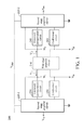
- FIG. 1 shows a block diagram of an operational amplifier circuit according to an embodiment of the invention
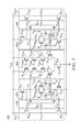
- FIG. 2 shows an exemplary circuit diagram of an operational amplifier circuit according to an embodiment of the invention
- FIG. 3 shows an exemplary circuit diagram of an operational amplifier circuit according to another embodiment of the invention.
- FIG. 4 shows a simulated phase margin of an operational amplifier circuit with and without the proposed feedforward path according to an embodiment of the invention.
- FIG. 1 shows a block diagram of an operational amplifier circuit according to an embodiment of the invention.
- the operational amplifier circuit 200 may comprise at least two stage amplifier circuits and frequency compensation circuits.
- the first stage amplifier circuit 210 may be coupled to a pair of differential input nodes of the operational amplifier circuit 200 for receiving a pair of differential input signals V in and V ip and amplifying the pair of differential input signals V in and V ip to generate amplified signals V 1 and V 2 respectively at nodes N 1 and N 2 .
- the second stage amplifier circuit may comprise two circuit subunits 220 - 1 and 220 - 2 and may be coupled to the first stage amplifier circuit 210 at the nodes N 1 and N 2 for receiving the amplified signals V 1 and V 2 from the first stage amplifier circuit 210 and further amplifying amplified signals V 1 and V 2 to respectively generate the output signals V op and V on , which may be a pair of differential output signals, at the output nodes of the operational amplifier circuit 200 .
- the frequency compensation circuits 230 and 240 may be operative to perform miller compensation for the frequency response of the operational amplifier circuit 200 .
- the operational amplifier circuit 200 may further comprise two feedforward circuits 250 and 260 , each being coupled between one of the input nodes of the operational amplifier circuit 200 and the second stage amplifier circuit for providing a feedforward path therebetween.
- the pair of differential input signals V in and V ip may be directly fed forward to the second stage amplifier circuit, which in the embodiment of the invention is the last stage amplifier circuit connected to the output nodes of the operational amplifier circuit 200 .
- feeding the input forward to the output may introduce one or more extra zeros in the overall transfer function of the operational amplifier circuit 200 . The extra zeros can be utilized to cancel the poles in the overall transfer function of the operational amplifier circuit 200 .
- the operational amplifier circuit 200 with the feedforward circuits may be designed as a class A amplifier or a class AB amplifier. Exemplary circuit diagrams of the proposed operational amplifier circuit will be discussed in detail in the following paragraphs.
- FIG. 2 shows an exemplary circuit diagram of an operational amplifier circuit according to an embodiment of the invention.
- the operational amplifier circuit 300 may comprise at least two stage amplifier circuits 310 and 320 - 1 and 320 - 2 , frequency compensation circuits 330 and 340 , and feedforward circuits 350 and 360 .
- the first stage amplifier circuit 310 may be coupled to a pair of differential input nodes of the operational amplifier circuit 300 for receiving a pair of differential input signals V in and V ip and amplifying the pair of differential input signals to respectively generate amplified signals at nodes N 1 and N 2 .
- the first stage amplifier circuit 310 may comprise a plurality of transistors M 0 ⁇ M 8 .
- the transistor M 0 may be coupled to a bias voltage V b1 .
- the pair of transistors M 1 and M 2 may be coupled to the input nodes of the operational amplifier circuit 300 for receiving the input signals V in and V ip .
- the pair of transistors M 3 and M 4 may be coupled to a bias voltage V casn .
- the pair of transistors M 5 and M 6 may be coupled to a bias voltage V casp .
- the pair of transistors M 7 and M 8 may be coupled to a bias voltage V CMFB , which is utilized to set the output common mode voltages of V op and V on
- the second stage amplifier circuit may comprise two circuit subunits 320 - 1 and 320 - 2 respectively coupled to the first stage amplifier circuit 310 at the nodes N 1 and N 2 for receiving the amplified signals from the first stage amplifier circuit 310 and further amplifying the amplified signals to respectively generate the output signals V op and V on at the output nodes of the operational amplifier circuit 300 .
- the circuit subunit 320 - 1 of the second stage amplifier circuit may comprise transistors M 9 and M 11 and the circuit subunit 320 - 2 of the second stage amplifier circuit may comprise transistors M 10 and M 12 .
- the transistor M 11 may be coupled between an operating voltage V DD and a first output node outputting the output signal V op .
- the transistor M 9 may be coupled between the first output node and a ground.
- the transistor M 12 may be coupled between the operating voltage V DD and a second output node outputting the output signal V on .
- the transistor M 10 may be coupled between the second output node and the ground.
- the output signals V op and V on may be a pair of differential output signals.
- the frequency compensation circuit 330 may comprise a capacitor C C1 and a resistor R C1 coupled in serial between the node N 1 and the first output node of the operational amplifier circuit 300 for performing miller compensation.
- the frequency compensation circuit 340 may comprise a capacitor C C2 and a resistor R C2 coupled in serial between the node N 2 and the second output node of the operational amplifier circuit 300 for performing miller compensation.
- the feedforward circuit 350 may comprise a feedforward capacitor C f1 with a first terminal coupled to a second input node receiving the input signal V in and a second terminal coupled to a gate of the transistor M 9 .
- the input signal V in is fed to the gate of the transistor M 9 via the feedforward capacitor C f1 .
- the feedforward circuit 360 may comprise a feedforward capacitor C f2 with a first terminal coupled to a first input node receiving the input signal V ip and a second terminal coupled to a gate of the transistor M 10 .
- the input signal V ip is fed to the gate of the transistor M 10 via the feedforward capacitor C f2 .
- the gate of the transistors M 9 and M 10 may be further coupled to a bias voltage V bnh and the capacitors C p1 and C p2 at the gate of the transistors M 9 and M 10 are the parasitic capacitors.
- feeding the input forward to the output may introduce extra zeros in the overall transfer function of the operational amplifier circuit 300 .
- the extra zeros can be utilized to cancel the poles in the overall transfer function of the operational amplifier circuit 300 . Therefore, introducing extra zeros can reduce the equivalent stages of the operational amplifier circuit 300 .
- the reduction of equivalent stages helps to stabilize the operational amplifier circuit 300 and may further extend the operation bandwidth of the operational amplifier circuit 300 .
- voltage swing will not be limited by the headroom of the transistors that are coupled to the source of the transistors M 9 and M 10 .
- the operation bandwidth of the operational amplifier circuit 300 may further be extended by making adjustment in the following three ways: 1) decreasing the capacitance of the capacitor C C1 and/or C C2 of the frequency compensation circuit(s), 2) increasing the current flowing through the transistors M 9 ⁇ M 12 of the second stage amplifier circuit, and 3) increasing the current flowing through the transistors M 0 , M 1 and M 2 of the first stage amplifier circuit. Because the designer may flexibly choose one or more adjustments to the capacitance and/or current to extend the operation bandwidth, the design freedom for bandwidth control can also be greatly improved as compared to conventional operational amplifier designs.
- FIG. 3 shows an exemplary circuit diagram of an operational amplifier circuit according to another embodiment of the invention.
- the operational amplifier circuit 400 may comprise at least two stage amplifier circuits 410 and 420 - 1 and 420 - 2 , frequency compensation circuits 430 and 440 , and feedforward circuits 450 and 460 .
- the first stage amplifier circuit 410 may be coupled to a pair of differential input nodes of the operational amplifier circuit 400 for receiving a pair of differential input signals V in and V ip and amplifying the pair of differential input signals to respectively generate amplified signals at nodes N 1 and N 2 .
- the first stage amplifier circuit 410 may comprise a plurality of transistors M c0 ⁇ M c8 .
- the transistor M c0 may be coupled to a bias voltage V b1 .
- the pair of transistors M c1 and M c2 may be coupled to the input nodes of the operational amplifier circuit 400 for receiving the input signals V in and V ip .
- the pair of transistors M c3 and M c4 may be coupled to a bias voltage V casn .
- the pair of transistors M c5 and M c6 may be coupled to a bias voltage V casp .
- the pair of transistors M c7 and M c8 may be coupled to a bias voltage V CMFB .
- the second stage amplifier circuit may comprise two circuit subunits 420 - 1 and 420 - 2 respectively coupled to the first stage amplifier circuit 410 at the nodes N 1 and N 2 for receiving the amplified signals from the first stage amplifier circuit 410 and further amplifying the amplified signals to respectively generate the output signals V op and V on at the output nodes of the operational amplifier circuit 400 .
- the circuit subunit 420 - 1 of the second stage amplifier circuit may comprise transistors M a1 and M a2
- the circuit subunit 420 - 2 of the second stage amplifier circuit may comprise transistors M b1 and M b2 .
- the transistor M a2 may be coupled between an operating voltage V DD and a first output node outputting the output signal V op .
- the transistor M a1 may be coupled between the first output node and a ground.
- the transistor M b2 may be coupled between the operating voltage V DD and a second output node outputting the output signal V on .
- the transistor M b1 may be coupled between the second output node and the ground.
- the output signals V op and V on may be a pair of differential output signals.
- the frequency compensation circuit 430 may be coupled between the first stage amplifier circuit 410 and the first output node and may comprise capacitors C C1 and C C2 and a resistor R C1 for performing miller compensation.
- the frequency compensation circuit 440 may be coupled between the first stage amplifier circuit 410 and the second output node and may comprise capacitors C C3 and C C4 and a resistor R C2 for performing miller compensation.
- the feedforward circuit 450 may comprise two feedforward capacitors C fa1 and C fa2 .
- the feedforward circuit 460 may comprise two feedforward capacitors C fb1 and C fb2 .
- the operational amplifier circuit 400 may further comprise two class AB controlling circuits 470 and 480 , which comprise static biasing transistors M a3 , M a4 , M b3 , and M b4 and dynamic biasing transistors M a5 , M a6 , M b5 , and M b6
- dynamic biasing transistors M a5 , M a6 , M b5 , and M b6 also act as the source follower input, which is favorable for high frequency application, and incur no noticeable stability degradation.
- the controlling circuit 470 which acts as a source follower in this embodiment may comprise a P-type source follower formed by transistors M a3 and M a5 and an N-type source follower formed by transistors M a4 and M a6 .
- the controlling circuit 480 which acts as a source follower in this embodiment may comprise a P-type source follower formed by transistors M b3 and M b5 and an N-type source follower formed by transistors M b4 and M b6 .
- a first terminal of the feedforward capacitor C fa1 may be coupled to the second input node of the operational amplifier circuit 400 for receiving the input signal V in and a second terminal of the feedforward capacitor C fa1 may be coupled to a gate of an input transistor M a5 of the P-type source follower formed by transistors M a3 and M a5 .
- the output terminal of the P-type source follower formed by transistors M a3 and M a5 may be coupled to a gate of the transistor M a2 of the second stage amplifier circuit at node N 1 .
- a first terminal of the feedforward capacitor C fa2 may also be coupled to the second input node of the operational amplifier circuit 400 for receiving the input signal V in and a second terminal of the feedforward capacitor C fa2 may be coupled to a gate of an input transistor M a6 of the N-type source follower formed by transistors M a4 and M a6 .
- the output terminal of the N-type source follower formed by transistors M a4 and M a6 may be coupled to a gate of the transistor M a1 of the second stage amplifier circuit at node N 3 .
- a first terminal of the feedforward capacitor C fb1 may be coupled to the first input node of the operational amplifier circuit 400 for receiving the input signal V ip and a second terminal of the feedforward capacitor C fb1 may be coupled to a gate of an input transistor M b5 of the P-type source follower formed by transistors M b3 and M b5 .
- the output terminal of the P-type source follower formed by transistors M b3 and M b5 may be coupled to a gate of the transistor M b2 of the second stage amplifier circuit at node N 2 .
- a first terminal of the feedforward capacitor C fb2 may also be coupled to the first input node of the operational amplifier circuit 400 for receiving the input signal V ip and a second terminal of the feedforward capacitor C fb2 may be coupled to a gate of an input transistor M b6 of the N-type source follower formed by transistors M b4 and M b6 .
- the output terminal of the N-type source follower formed by transistors M b4 and M b6 may be coupled to a gate of the transistor M b1 of the second stage amplifier circuit at node N 4 .
- the input terminal of the P-type source follower formed by transistors M a3 and M a5 is coupled to the feedforward capacitor C fa1 for receiving the input signal V in therethrough and the output terminal of the P-type source follower is coupled to the gate of the transistor M a2 at node N 1 , the input signal V in can be fed to the gate of the transistor M a2 via the feedforward capacitor C fa1 and the P-type source follower.
- the input terminal of the N-type source follower formed by transistors M a4 and M a6 is coupled to the feedforward capacitor C fa2 for receiving the input signal V in therethrough and the output terminal of the N-type source follower is coupled to the gate of the transistor M a1 at node N 3 , the input signal V in can also be fed to the gate of the transistor M a1 via the feedforward capacitor C fa2 and the N-type source follower.
- the input terminal of the P-type source follower formed by transistors M b3 and M b5 is coupled to the feedforward capacitor C fb1 for receiving the input signal V ip therethrough and the output terminal of the P-type source follower is coupled to the gate of the transistor M b2 at node N 2 , the input signal V ip can be fed to the gate of the transistor M b2 via the feedforward capacitor C fb1 and the P-type source follower.
- the input terminal of the N-type source follower formed by transistors M b4 and M b6 is coupled to the feedforward capacitor C fb2 for receiving the input signal V ip therethrough and the output terminal of the N-type source follower is coupled to the gate of the transistor M b1 at node N 4 , the input signal V ip can also be fed to the gate of the transistor M b1 via the feedforward capacitor C fb2 and the N-type source follower.
- the gate of the transistor M a5 and the gate of the transistor M b5 may be further coupled to a bias voltage V bp and the gate of the transistor M a6 and the gate of the transistor M b6 may be further coupled to a bias voltage V bn .
- the gate of the transistor M a4 and the gate of the transistor M b4 may be coupled to the bias voltage V b1 and the gate of the transistor M a3 and the gate of the transistor M b3 may be coupled to a bias voltage V b2 .
- the source follower circuits e.g., the class AB controlling circuits 470 and 480
- the source follower circuits may be integrated in the first stage amplifier circuit 410 to become a portion of the first stage amplifier and therefore the invention should not be limited thereto.
- feeding the input forward to the output may introduce extra zeros in the overall transfer function of the operational amplifier circuit 400 .
- the extra zeros can be utilized to cancel the poles in the overall transfer function of the operational amplifier circuit 400 . Therefore, introducing extra zeros can reduce the equivalent stages of the operational amplifier circuit 400 .
- the reduction of equivalent stages helps to stabilize the operational amplifier circuit 400 and may further extend the operation bandwidth of the operational amplifier circuit 400 .
- the common mode voltages are determined by the transistors M c7 and M c8 through the adjusting mechanism of bias voltage V CMFB . Therefore, linearity of the proposed operational amplifier circuit 400 as shown in FIG. 3 can be greatly improved because there is only one device coupled between output node and V DD or that and ground.
- the operation bandwidth of the operational amplifier circuit 400 may be further extended by making adjustments in the following three ways: 1) decreasing the capacitance of the capacitor C C1 , C C2 , C C3 and/or C C4 in the frequency compensation circuit(s), 2) increasing the current flowing through the transistors M a1 , M a2 , M b1 and/or M b2 of the second stage amplifier circuit, and 3) increasing the current flowing through the transistors M c0 , M c1 and M c2 of the first stage amplifier circuit. Because the designer may flexibly choose one or more adjustments to the capacitance and/or current to extend the operation bandwidth, the design freedom for bandwidth control can also be greatly improved as compared to conventional operational amplifier designs.
- FIG. 4 shows a simulated phase margin of an operational amplifier circuit with and without the proposed feedforward path according to an embodiment of the invention.
- the simulated phase margin of an operational amplifier circuit with the proposed feedforward path can be dramatically improved as compared to a conventional two stage operational amplifier, especially in the high frequency area, due to the ac coupling path(s) provided by the feedforward circuit(s). Therefore, the proposed operational amplifier circuits serve as good candidates to achieve high linearity and the design flexibility, as previously described, is high in high-frequency applications.
Landscapes
- Engineering & Computer Science (AREA)
- Power Engineering (AREA)
- Physics & Mathematics (AREA)
- Nonlinear Science (AREA)
- Amplifiers (AREA)
Abstract
Description
- This application claims the benefit of U.S. Provisional Application No. 61/596,356 filed 2012 Feb. 8, the entire contents of which are hereby incorporated by reference.
- 1. Field of the Invention
- The invention relates to a high-speed operational amplifier circuit, and more particularly to a high-speed operational amplifier circuit having high linearity and design freedom.
- 2. Description of the Related Art
- Using high-speed operational amplifier is a trend in high-frequency (for example, several GHz) applications. When designing a high-speed operational amplifier, transconductance(s) may be used in the operational amplifier circuit to extend operation bandwidth of the operational amplifier. However, it may be power inefficient for an application bandwidth larger than several GHz since the parasitic poles may cause the operational amplifier to become unstable and more current may be needed to stabilize it.
- Since using the high-speed operational amplifier is a trend in high-frequency (for example, several GHz) applications, a novel high-speed operational amplifier circuit which is more stable and has lower power consumption than the conventional designs, and which further has high linearity and design freedom, is highly desired.
- Operational amplifier circuits are provided. An exemplary embodiment of an operational amplifier circuit comprises a first stage amplifier circuit, a second stage amplifier circuit, and a first feedforward circuit. The first stage amplifier circuit is coupled to an input node for receiving an input signal and amplifying the input signal to generate an amplified signal. The second stage amplifier circuit is coupled to the first stage amplifier circuit for receiving the amplified signal and amplifying the amplified signal to generate an output signal at an output node. The first feedforward circuit is coupled between the input node and the second stage amplifier circuit for feeding the input signal forward to the second stage amplifier circuit.
- Another exemplary embodiment of an operational amplifier circuit comprises a first stage amplifier circuit, a second stage amplifier circuit, a first feedforward circuit and a second feedforward circuit. The first stage amplifier circuit is coupled to a first input node and a second input node for receiving a first input signal and a second input signal, amplifying the first input signal to generate a first amplified signal and amplifying the second input signal to generate a second amplified signal. The second stage amplifier circuit is coupled to the first stage amplifier circuit for receiving and amplifying the first amplified signal and the second amplified signal to generate a first output signal at a first output node and a second output signal at a second output node. The second stage amplifier circuit comprises a first transistor coupled between an operating voltage and the first output node, a second transistor coupled between the first output node and a ground, a third transistor coupled between the operating voltage and the second output node, and a fourth transistor coupled between the second output node and the ground. The first feedforward circuit is coupled between the first input node and a gate of the second transistor for feeding the first input signal forward to the gate of the second transistor. The second feedforward circuit is coupled between the second input node and a gate of the fourth transistor for feeding the second input signal forward to the gate of the fourth transistor.
- A detailed description is given in the following embodiments with reference to the accompanying drawings.
- The invention can be more fully understood by reading the subsequent detailed description and examples with references made to the accompanying drawings, wherein:
-
FIG. 1 shows a block diagram of an operational amplifier circuit according to an embodiment of the invention; -
FIG. 2 shows an exemplary circuit diagram of an operational amplifier circuit according to an embodiment of the invention; -
FIG. 3 shows an exemplary circuit diagram of an operational amplifier circuit according to another embodiment of the invention; and -
FIG. 4 shows a simulated phase margin of an operational amplifier circuit with and without the proposed feedforward path according to an embodiment of the invention. - The following description is of the best-contemplated mode of carrying out the invention. This description is made for the purpose of illustrating the general principles of the invention and should not be taken in a limiting sense. The scope of the invention is best determined by reference to the appended claims.
-
FIG. 1 shows a block diagram of an operational amplifier circuit according to an embodiment of the invention. According to an embodiment of the invention, theoperational amplifier circuit 200 may comprise at least two stage amplifier circuits and frequency compensation circuits. The firststage amplifier circuit 210 may be coupled to a pair of differential input nodes of theoperational amplifier circuit 200 for receiving a pair of differential input signals Vin and Vip and amplifying the pair of differential input signals Vin and Vip to generate amplified signals V1 and V2 respectively at nodes N1 and N2. The second stage amplifier circuit may comprise two circuit subunits 220-1 and 220-2 and may be coupled to the firststage amplifier circuit 210 at the nodes N1 and N2 for receiving the amplified signals V1 and V2 from the firststage amplifier circuit 210 and further amplifying amplified signals V1 and V2 to respectively generate the output signals Vop and Von, which may be a pair of differential output signals, at the output nodes of theoperational amplifier circuit 200. Thefrequency compensation circuits operational amplifier circuit 200. - According to an embodiment of the invention, the
operational amplifier circuit 200 may further comprise twofeedforward circuits operational amplifier circuit 200 and the second stage amplifier circuit for providing a feedforward path therebetween. Via thefeedforward circuits operational amplifier circuit 200. According to an embodiment of the invention, feeding the input forward to the output may introduce one or more extra zeros in the overall transfer function of theoperational amplifier circuit 200. The extra zeros can be utilized to cancel the poles in the overall transfer function of theoperational amplifier circuit 200. Therefore, introducing extra zeros can reduce the equivalent stages of theoperational amplifier circuit 200. The reduction of equivalent stages helps to stabilize theoperational amplifier circuit 200 and may further extend the operation bandwidth of theoperational amplifier circuit 200. Eventually, the order at high frequency of the operational amplifier circuit is reduced to one, which manifests itself as a powerful structure for high frequency application since the stability is easy to be handled. According to the embodiments of the invention, theoperational amplifier circuit 200 with the feedforward circuits may be designed as a class A amplifier or a class AB amplifier. Exemplary circuit diagrams of the proposed operational amplifier circuit will be discussed in detail in the following paragraphs. -
FIG. 2 shows an exemplary circuit diagram of an operational amplifier circuit according to an embodiment of the invention. According to the embodiment of the invention, theoperational amplifier circuit 300 may comprise at least twostage amplifier circuits 310 and 320-1 and 320-2,frequency compensation circuits feedforward circuits stage amplifier circuit 310 may be coupled to a pair of differential input nodes of theoperational amplifier circuit 300 for receiving a pair of differential input signals Vin and Vip and amplifying the pair of differential input signals to respectively generate amplified signals at nodes N1 and N2. The firststage amplifier circuit 310 may comprise a plurality of transistors M0˜M8. The transistor M0 may be coupled to a bias voltage Vb1. The pair of transistors M1 and M2 may be coupled to the input nodes of theoperational amplifier circuit 300 for receiving the input signals Vin and Vip. The pair of transistors M3 and M4 may be coupled to a bias voltage Vcasn. The pair of transistors M5 and M6 may be coupled to a bias voltage Vcasp. The pair of transistors M7 and M8 may be coupled to a bias voltage VCMFB, which is utilized to set the output common mode voltages of Vop and Von - The second stage amplifier circuit may comprise two circuit subunits 320-1 and 320-2 respectively coupled to the first
stage amplifier circuit 310 at the nodes N1 and N2 for receiving the amplified signals from the firststage amplifier circuit 310 and further amplifying the amplified signals to respectively generate the output signals Vop and Von at the output nodes of theoperational amplifier circuit 300. The circuit subunit 320-1 of the second stage amplifier circuit may comprise transistors M9 and M11 and the circuit subunit 320-2 of the second stage amplifier circuit may comprise transistors M10 and M12. The transistor M11 may be coupled between an operating voltage VDD and a first output node outputting the output signal Vop. The transistor M9 may be coupled between the first output node and a ground. The transistor M12 may be coupled between the operating voltage VDD and a second output node outputting the output signal Von. The transistor M10 may be coupled between the second output node and the ground. According to an embodiment of the invention, the output signals Vop and Von may be a pair of differential output signals. - The
frequency compensation circuit 330 may comprise a capacitor CC1 and a resistor RC1 coupled in serial between the node N1 and the first output node of theoperational amplifier circuit 300 for performing miller compensation. Thefrequency compensation circuit 340 may comprise a capacitor CC2 and a resistor RC2 coupled in serial between the node N2 and the second output node of theoperational amplifier circuit 300 for performing miller compensation. - The
feedforward circuit 350 may comprise a feedforward capacitor Cf1 with a first terminal coupled to a second input node receiving the input signal Vin and a second terminal coupled to a gate of the transistor M9. According to an embodiment of the invention, the input signal Vin is fed to the gate of the transistor M9 via the feedforward capacitor Cf1. Thefeedforward circuit 360 may comprise a feedforward capacitor Cf2 with a first terminal coupled to a first input node receiving the input signal Vip and a second terminal coupled to a gate of the transistor M10. According to an embodiment of the invention, the input signal Vip is fed to the gate of the transistor M10 via the feedforward capacitor Cf2. According to an embodiment of the invention, the gate of the transistors M9 and M10 may be further coupled to a bias voltage Vbnh and the capacitors Cp1 and Cp2 at the gate of the transistors M9 and M10 are the parasitic capacitors. - As previously described, feeding the input forward to the output may introduce extra zeros in the overall transfer function of the
operational amplifier circuit 300. The extra zeros can be utilized to cancel the poles in the overall transfer function of theoperational amplifier circuit 300. Therefore, introducing extra zeros can reduce the equivalent stages of theoperational amplifier circuit 300. The reduction of equivalent stages helps to stabilize theoperational amplifier circuit 300 and may further extend the operation bandwidth of theoperational amplifier circuit 300. In addition, in the embodiments of the invention, because there are only four transistors in the second stage amplifier circuit, in which transistors M9 and M10 receiving the fed-forward input signals Vin and Vip are directly coupled to the ground, voltage swing will not be limited by the headroom of the transistors that are coupled to the source of the transistors M9 and M10. In other words, in the proposed operational amplifier circuit as shown inFIG. 2 , there is no extra transistor, which may conventionally be utilized to provide appropriate common mode voltages for the output nodes Vop and Von, coupled to the source of the transistors M9 and M10. Instead, the common mode voltages are determined by the transistors M7 and M8 through the adjusting mechanism of bias voltage VCMFB. Therefore, linearity of the proposedoperational amplifier circuit 300 as shown inFIG. 2 can be greatly improved because there is only one device coupled between output node and VDD or that and ground. - In addition, the operation bandwidth of the
operational amplifier circuit 300 may further be extended by making adjustment in the following three ways: 1) decreasing the capacitance of the capacitor CC1 and/or CC2 of the frequency compensation circuit(s), 2) increasing the current flowing through the transistors M9˜M12 of the second stage amplifier circuit, and 3) increasing the current flowing through the transistors M0, M1 and M2 of the first stage amplifier circuit. Because the designer may flexibly choose one or more adjustments to the capacitance and/or current to extend the operation bandwidth, the design freedom for bandwidth control can also be greatly improved as compared to conventional operational amplifier designs. -
FIG. 3 shows an exemplary circuit diagram of an operational amplifier circuit according to another embodiment of the invention. According to the embodiment of the invention, theoperational amplifier circuit 400 may comprise at least twostage amplifier circuits 410 and 420-1 and 420-2,frequency compensation circuits feedforward circuits stage amplifier circuit 410 may be coupled to a pair of differential input nodes of theoperational amplifier circuit 400 for receiving a pair of differential input signals Vin and Vip and amplifying the pair of differential input signals to respectively generate amplified signals at nodes N1 and N2. The firststage amplifier circuit 410 may comprise a plurality of transistors Mc0˜Mc8. The transistor Mc0 may be coupled to a bias voltage Vb1. The pair of transistors Mc1 and Mc2 may be coupled to the input nodes of theoperational amplifier circuit 400 for receiving the input signals Vin and Vip. The pair of transistors Mc3 and Mc4 may be coupled to a bias voltage Vcasn. The pair of transistors Mc5 and Mc6 may be coupled to a bias voltage Vcasp. The pair of transistors Mc7 and Mc8 may be coupled to a bias voltage VCMFB. - The second stage amplifier circuit may comprise two circuit subunits 420-1 and 420-2 respectively coupled to the first
stage amplifier circuit 410 at the nodes N1 and N2 for receiving the amplified signals from the firststage amplifier circuit 410 and further amplifying the amplified signals to respectively generate the output signals Vop and Von at the output nodes of theoperational amplifier circuit 400. The circuit subunit 420-1 of the second stage amplifier circuit may comprise transistors Ma1 and Ma2, and the circuit subunit 420-2 of the second stage amplifier circuit may comprise transistors Mb1 and Mb2. The transistor Ma2 may be coupled between an operating voltage VDD and a first output node outputting the output signal Vop. The transistor Ma1 may be coupled between the first output node and a ground. The transistor Mb2 may be coupled between the operating voltage VDD and a second output node outputting the output signal Von. The transistor Mb1 may be coupled between the second output node and the ground. According to an embodiment of the invention, the output signals Vop and Von may be a pair of differential output signals. - The
frequency compensation circuit 430 may be coupled between the firststage amplifier circuit 410 and the first output node and may comprise capacitors CC1 and CC2 and a resistor RC1 for performing miller compensation. Thefrequency compensation circuit 440 may be coupled between the firststage amplifier circuit 410 and the second output node and may comprise capacitors CC3 and CC4 and a resistor RC2 for performing miller compensation. - The
feedforward circuit 450 may comprise two feedforward capacitors Cfa1 and Cfa2. Thefeedforward circuit 460 may comprise two feedforward capacitors Cfb1 and Cfb2. According to an embodiment of the invention, theoperational amplifier circuit 400 may further comprise two classAB controlling circuits controlling circuit 470 which acts as a source follower in this embodiment may comprise a P-type source follower formed by transistors Ma3 and Ma5 and an N-type source follower formed by transistors Ma4 and Ma6.The controlling circuit 480 which acts as a source follower in this embodiment may comprise a P-type source follower formed by transistors Mb3 and Mb5 and an N-type source follower formed by transistors Mb4 and Mb6. - According to an embodiment of the invention, a first terminal of the feedforward capacitor Cfa1 may be coupled to the second input node of the
operational amplifier circuit 400 for receiving the input signal Vin and a second terminal of the feedforward capacitor Cfa1 may be coupled to a gate of an input transistor Ma5 of the P-type source follower formed by transistors Ma3 and Ma5. The output terminal of the P-type source follower formed by transistors Ma3 and Ma5 may be coupled to a gate of the transistor Ma2 of the second stage amplifier circuit at node N1. In addition, a first terminal of the feedforward capacitor Cfa2 may also be coupled to the second input node of theoperational amplifier circuit 400 for receiving the input signal Vin and a second terminal of the feedforward capacitor Cfa2 may be coupled to a gate of an input transistor Ma6 of the N-type source follower formed by transistors Ma4 and Ma6. The output terminal of the N-type source follower formed by transistors Ma4 and Ma6 may be coupled to a gate of the transistor Ma1 of the second stage amplifier circuit at node N3. - Similarly, a first terminal of the feedforward capacitor Cfb1 may be coupled to the first input node of the
operational amplifier circuit 400 for receiving the input signal Vip and a second terminal of the feedforward capacitor Cfb1 may be coupled to a gate of an input transistor Mb5 of the P-type source follower formed by transistors Mb3 and Mb5. The output terminal of the P-type source follower formed by transistors Mb3 and Mb5 may be coupled to a gate of the transistor Mb2 of the second stage amplifier circuit at node N2. In addition, a first terminal of the feedforward capacitor Cfb2 may also be coupled to the first input node of theoperational amplifier circuit 400 for receiving the input signal Vip and a second terminal of the feedforward capacitor Cfb2 may be coupled to a gate of an input transistor Mb6 of the N-type source follower formed by transistors Mb4 and Mb6. The output terminal of the N-type source follower formed by transistors Mb4 and Mb6 may be coupled to a gate of the transistor Mb1 of the second stage amplifier circuit at node N4. - According to an embodiment of the invention, because the input terminal of the P-type source follower formed by transistors Ma3 and Ma5 is coupled to the feedforward capacitor Cfa1 for receiving the input signal Vin therethrough and the output terminal of the P-type source follower is coupled to the gate of the transistor Ma2 at node N1, the input signal Vin can be fed to the gate of the transistor Ma2 via the feedforward capacitor Cfa1 and the P-type source follower. In addition, because the input terminal of the N-type source follower formed by transistors Ma4 and Ma6 is coupled to the feedforward capacitor Cfa2 for receiving the input signal Vin therethrough and the output terminal of the N-type source follower is coupled to the gate of the transistor Ma1 at node N3, the input signal Vin can also be fed to the gate of the transistor Ma1 via the feedforward capacitor Cfa2 and the N-type source follower.
- Similarly, according to an embodiment of the invention, because the input terminal of the P-type source follower formed by transistors Mb3 and Mb5 is coupled to the feedforward capacitor Cfb1 for receiving the input signal Vip therethrough and the output terminal of the P-type source follower is coupled to the gate of the transistor Mb2 at node N2, the input signal Vip can be fed to the gate of the transistor Mb2 via the feedforward capacitor Cfb1 and the P-type source follower. In addition, because the input terminal of the N-type source follower formed by transistors Mb4 and Mb6 is coupled to the feedforward capacitor Cfb2 for receiving the input signal Vip therethrough and the output terminal of the N-type source follower is coupled to the gate of the transistor Mb1 at node N4, the input signal Vip can also be fed to the gate of the transistor Mb1 via the feedforward capacitor Cfb2 and the N-type source follower.
- According to an embodiment of the invention, the gate of the transistor Ma5 and the gate of the transistor Mb5 may be further coupled to a bias voltage Vbp and the gate of the transistor Ma6 and the gate of the transistor Mb6 may be further coupled to a bias voltage Vbn. In addition, the gate of the transistor Ma4 and the gate of the transistor Mb4 may be coupled to the bias voltage Vb1 and the gate of the transistor Ma3 and the gate of the transistor Mb3 may be coupled to a bias voltage Vb2. Note that according to some embodiments of the invention, the source follower circuits (e.g., the class
AB controlling circuits 470 and 480) may be integrated in the firststage amplifier circuit 410 to become a portion of the first stage amplifier and therefore the invention should not be limited thereto. - As previously described, feeding the input forward to the output may introduce extra zeros in the overall transfer function of the
operational amplifier circuit 400. The extra zeros can be utilized to cancel the poles in the overall transfer function of theoperational amplifier circuit 400. Therefore, introducing extra zeros can reduce the equivalent stages of theoperational amplifier circuit 400. The reduction of equivalent stages helps to stabilize theoperational amplifier circuit 400 and may further extend the operation bandwidth of theoperational amplifier circuit 400. In addition, in the embodiments of the invention, because there are only four transistors in the second stage amplifier circuit, in which the transistors Ma1 and Mb1 receiving the fed-forward input signals Vin and Vip are directly coupled to the ground, voltage swing will not be limited by the headroom of the transistors that are coupled to the source of the transistors Ma1 and Mb1. In other words, in the proposed operational amplifier circuit as shown inFIG. 3 , there is no extra transistor, which may conventionally utilized to provide appropriate common mode voltages for the output nodes Vop and Von, coupled to the source of the transistors Ma1 and Mb1. Instead, the common mode voltages are determined by the transistors Mc7 and Mc8 through the adjusting mechanism of bias voltage VCMFB. Therefore, linearity of the proposedoperational amplifier circuit 400 as shown inFIG. 3 can be greatly improved because there is only one device coupled between output node and VDD or that and ground. - In addition, the operation bandwidth of the
operational amplifier circuit 400 may be further extended by making adjustments in the following three ways: 1) decreasing the capacitance of the capacitor CC1, CC2, CC3 and/or CC4 in the frequency compensation circuit(s), 2) increasing the current flowing through the transistors Ma1, Ma2, Mb1 and/or Mb2 of the second stage amplifier circuit, and 3) increasing the current flowing through the transistors Mc0, Mc1 and Mc2 of the first stage amplifier circuit. Because the designer may flexibly choose one or more adjustments to the capacitance and/or current to extend the operation bandwidth, the design freedom for bandwidth control can also be greatly improved as compared to conventional operational amplifier designs. -
FIG. 4 shows a simulated phase margin of an operational amplifier circuit with and without the proposed feedforward path according to an embodiment of the invention. As shown inFIG. 4 , the simulated phase margin of an operational amplifier circuit with the proposed feedforward path can be dramatically improved as compared to a conventional two stage operational amplifier, especially in the high frequency area, due to the ac coupling path(s) provided by the feedforward circuit(s). Therefore, the proposed operational amplifier circuits serve as good candidates to achieve high linearity and the design flexibility, as previously described, is high in high-frequency applications. - While the invention has been described by way of example and in terms of preferred embodiment, it is to be understood that the invention is not limited thereto. Those who are skilled in this technology can still make various alterations and modifications without departing from the scope and spirit of this invention. Therefore, the scope of the present invention shall be defined and protected by the following claims and their equivalents.
Claims (19)
Priority Applications (3)
| Application Number | Priority Date | Filing Date | Title |
|---|---|---|---|
| US13/612,784 US8890611B2 (en) | 2012-02-08 | 2012-09-12 | Operational amplifier circuits |
| CN201310016756.0A CN103338014B (en) | 2012-02-08 | 2013-01-17 | Operational Amplifier Circuit |
| US14/513,387 US9628035B2 (en) | 2012-02-08 | 2014-10-14 | Operational amplifier circuits |
Applications Claiming Priority (2)
| Application Number | Priority Date | Filing Date | Title |
|---|---|---|---|
| US201261596356P | 2012-02-08 | 2012-02-08 | |
| US13/612,784 US8890611B2 (en) | 2012-02-08 | 2012-09-12 | Operational amplifier circuits |
Related Child Applications (1)
| Application Number | Title | Priority Date | Filing Date |
|---|---|---|---|
| US14/513,387 Continuation US9628035B2 (en) | 2012-02-08 | 2014-10-14 | Operational amplifier circuits |
Publications (2)
| Publication Number | Publication Date |
|---|---|
| US20130200953A1 true US20130200953A1 (en) | 2013-08-08 |
| US8890611B2 US8890611B2 (en) | 2014-11-18 |
Family
ID=48902372
Family Applications (2)
| Application Number | Title | Priority Date | Filing Date |
|---|---|---|---|
| US13/612,784 Active 2032-10-24 US8890611B2 (en) | 2012-02-08 | 2012-09-12 | Operational amplifier circuits |
| US14/513,387 Active 2032-09-13 US9628035B2 (en) | 2012-02-08 | 2014-10-14 | Operational amplifier circuits |
Family Applications After (1)
| Application Number | Title | Priority Date | Filing Date |
|---|---|---|---|
| US14/513,387 Active 2032-09-13 US9628035B2 (en) | 2012-02-08 | 2014-10-14 | Operational amplifier circuits |
Country Status (2)
| Country | Link |
|---|---|
| US (2) | US8890611B2 (en) |
| CN (1) | CN103338014B (en) |
Cited By (6)
| Publication number | Priority date | Publication date | Assignee | Title |
|---|---|---|---|---|
| CN107196616A (en) * | 2017-05-30 | 2017-09-22 | 长沙方星腾电子科技有限公司 | A kind of Miller's compensating circuit and operational amplifier for operational amplifier |
| EP3355471A1 (en) * | 2017-01-25 | 2018-08-01 | MediaTek Inc. | Class ab amplifier having cascode stage with filter for improving linearity |
| KR20210096623A (en) * | 2018-12-05 | 2021-08-05 | 페르디난드-브라운-인스티튜트 게게엠바하, 라이브니츠-인스티튜트 푸어 훼스트후리퀀즈테크닉 | High-frequency power transistors and high-frequency power amplifiers |
| KR20210101852A (en) * | 2020-02-11 | 2021-08-19 | 숭실대학교산학협력단 | Power Amplifier |
| CN113395048A (en) * | 2020-03-11 | 2021-09-14 | 中国电子科技集团公司第二十四研究所 | Mixed compensation three-stage operational amplifier |
| CN113452332A (en) * | 2020-03-27 | 2021-09-28 | 爱思开海力士有限公司 | Differential amplifier |
Families Citing this family (10)
| Publication number | Priority date | Publication date | Assignee | Title |
|---|---|---|---|---|
| US8890611B2 (en) * | 2012-02-08 | 2014-11-18 | Mediatek Inc. | Operational amplifier circuits |
| JP2015220689A (en) * | 2014-05-20 | 2015-12-07 | 富士通株式会社 | Differential amplifier circuit |
| CN104283519B (en) * | 2014-10-24 | 2017-06-09 | 中国电子科技集团公司第十三研究所 | Current multiplexing type feedforward compensation Full differential operational amplifier |
| CN104393846B (en) * | 2014-11-17 | 2018-02-06 | 上海华虹宏力半导体制造有限公司 | Operational amplifier |
| CN105099451B (en) * | 2015-07-31 | 2018-06-15 | 华为技术有限公司 | Differential amplifier circuit and the production line analog-digital converter using the differential amplifier circuit |
| US10187024B2 (en) | 2016-05-09 | 2019-01-22 | Mediatek Inc. | Input feed-forward technique for class AB amplifier |
| KR102558000B1 (en) | 2018-03-27 | 2023-07-20 | 삼성전자주식회사 | Amplifying circuit comprising miller compensation circuit |
| KR102772414B1 (en) | 2019-10-07 | 2025-02-25 | 삼성전자주식회사 | Fully differential amplifier including feedforward path |
| CN114967826B (en) * | 2021-02-26 | 2024-04-16 | 瑞昱半导体股份有限公司 | Low-dropout voltage regulator |
| CN118694321A (en) * | 2023-03-24 | 2024-09-24 | 华为技术有限公司 | Operational amplifiers, chips, electronic devices |
Citations (1)
| Publication number | Priority date | Publication date | Assignee | Title |
|---|---|---|---|---|
| US5216380A (en) * | 1990-10-05 | 1993-06-01 | Texas Instruments Incorporated | Performance operational amplifier and method of amplification |
Family Cites Families (8)
| Publication number | Priority date | Publication date | Assignee | Title |
|---|---|---|---|---|
| JP2892287B2 (en) * | 1994-02-04 | 1999-05-17 | 松下電器産業株式会社 | Operational amplifier |
| SE519691C2 (en) | 1997-07-08 | 2003-04-01 | Ericsson Telefon Ab L M | High speed and high gain operational amplifier |
| JP2005045702A (en) | 2003-07-25 | 2005-02-17 | Matsushita Electric Ind Co Ltd | Differential amplifier and test circuit with differential amplifier |
| KR100674912B1 (en) * | 2004-09-24 | 2007-01-26 | 삼성전자주식회사 | Differential Amplification Circuit with Improved Slew Rate |
| US7504886B2 (en) * | 2006-09-11 | 2009-03-17 | Lecroy Corporation | Thermal tail compensation |
| US7852158B2 (en) | 2006-11-30 | 2010-12-14 | Panasonic Corporation | Operational amplifier |
| CN101635560A (en) * | 2009-08-26 | 2010-01-27 | 余浩 | High-speed two-stage calculation amplifier |
| US8890611B2 (en) * | 2012-02-08 | 2014-11-18 | Mediatek Inc. | Operational amplifier circuits |
-
2012
- 2012-09-12 US US13/612,784 patent/US8890611B2/en active Active
-
2013
- 2013-01-17 CN CN201310016756.0A patent/CN103338014B/en active Active
-
2014
- 2014-10-14 US US14/513,387 patent/US9628035B2/en active Active
Patent Citations (1)
| Publication number | Priority date | Publication date | Assignee | Title |
|---|---|---|---|---|
| US5216380A (en) * | 1990-10-05 | 1993-06-01 | Texas Instruments Incorporated | Performance operational amplifier and method of amplification |
Cited By (11)
| Publication number | Priority date | Publication date | Assignee | Title |
|---|---|---|---|---|
| EP3355471A1 (en) * | 2017-01-25 | 2018-08-01 | MediaTek Inc. | Class ab amplifier having cascode stage with filter for improving linearity |
| CN107196616A (en) * | 2017-05-30 | 2017-09-22 | 长沙方星腾电子科技有限公司 | A kind of Miller's compensating circuit and operational amplifier for operational amplifier |
| KR20210096623A (en) * | 2018-12-05 | 2021-08-05 | 페르디난드-브라운-인스티튜트 게게엠바하, 라이브니츠-인스티튜트 푸어 훼스트후리퀀즈테크닉 | High-frequency power transistors and high-frequency power amplifiers |
| KR102795974B1 (en) * | 2018-12-05 | 2025-04-14 | 페르디난드-브라운-인스티튜트 게게엠바하, 라이브니츠-인스티튜트 푸어 훼스트후리퀀즈테크닉 | High frequency power transistors and high frequency power amplifiers |
| KR20210101852A (en) * | 2020-02-11 | 2021-08-19 | 숭실대학교산학협력단 | Power Amplifier |
| KR102449479B1 (en) * | 2020-02-11 | 2022-09-30 | 숭실대학교산학협력단 | power amplifier |
| CN113395048A (en) * | 2020-03-11 | 2021-09-14 | 中国电子科技集团公司第二十四研究所 | Mixed compensation three-stage operational amplifier |
| CN113452332A (en) * | 2020-03-27 | 2021-09-28 | 爱思开海力士有限公司 | Differential amplifier |
| KR20210120506A (en) * | 2020-03-27 | 2021-10-07 | 에스케이하이닉스 주식회사 | Differential amplifier circuit |
| US11489500B2 (en) * | 2020-03-27 | 2022-11-01 | SK Hynix Inc. | Differential amplifier |
| KR102813465B1 (en) * | 2020-03-27 | 2025-05-27 | 에스케이하이닉스 주식회사 | Differential amplifier circuit |
Also Published As
| Publication number | Publication date |
|---|---|
| US20150028951A1 (en) | 2015-01-29 |
| US8890611B2 (en) | 2014-11-18 |
| CN103338014A (en) | 2013-10-02 |
| US9628035B2 (en) | 2017-04-18 |
| CN103338014B (en) | 2016-04-06 |
Similar Documents
| Publication | Publication Date | Title |
|---|---|---|
| US9628035B2 (en) | Operational amplifier circuits | |
| US7859338B2 (en) | Compact low-power class AB amplifier | |
| US7733182B2 (en) | Hybrid class AB super follower | |
| US20080272844A1 (en) | Class ab folded-cascode amplifier having cascode compensation | |
| CN101242160B (en) | Two-stage operational amplifier with class ab output stage | |
| US6300834B1 (en) | High performance intermediate stage circuit for a rail-to-rail input/output CMOS operational amplifier | |
| US8836427B2 (en) | Folded cascode operational amplifier | |
| US7271663B2 (en) | Operational amplifier output stage and method | |
| Sarkar et al. | Design of a power efficient, high slew rate and gain boosted improved recycling folded cascode amplifier with adaptive biasing technique | |
| US20220263480A1 (en) | Operational amplifier using single-stage amplifier with slew-rate enhancement and associated method | |
| US6833760B1 (en) | Low power differential amplifier powered by multiple unequal power supply voltages | |
| US9214898B2 (en) | Triple cascode power amplifier | |
| US11329619B2 (en) | Operational amplifier | |
| TWI504139B (en) | Operational amplifier circuit | |
| US20050200411A1 (en) | Differential amplifier without common mode feedback | |
| US20140292410A1 (en) | Folded cascode amplifier circuit | |
| US11496105B2 (en) | Multi-stage amplifier circuit | |
| US7834693B2 (en) | Amplifying circuit | |
| Neag et al. | Design options for high-speed OA-based fully differential buffers able to drive large loads | |
| Ali | A power efficient gain enhancing technique for current mirror operational transconductance amplifiers | |
| CN115314011B (en) | With feedforward compensated amplifier | |
| US11848649B2 (en) | Low power VB class AB amplifier with local common mode feedback | |
| US10187024B2 (en) | Input feed-forward technique for class AB amplifier | |
| US7443238B2 (en) | Amplifier stage, operational amplifier and method for amplifying a signal | |
| CN110768636A (en) | Stability compensation method and circuit structure for multistage operational amplifier |
Legal Events
| Date | Code | Title | Description |
|---|---|---|---|
| AS | Assignment |
Owner name: MEDIATEK INC., TAIWAN Free format text: ASSIGNMENT OF ASSIGNORS INTEREST;ASSIGNORS:TSAI, HUNG-CHIEH;LO, CHI-LUN;HO, CHEN-YEN;AND OTHERS;REEL/FRAME:029889/0144 Effective date: 20130221 |
|
| STCF | Information on status: patent grant |
Free format text: PATENTED CASE |
|
| MAFP | Maintenance fee payment |
Free format text: PAYMENT OF MAINTENANCE FEE, 4TH YEAR, LARGE ENTITY (ORIGINAL EVENT CODE: M1551) Year of fee payment: 4 |
|
| MAFP | Maintenance fee payment |
Free format text: PAYMENT OF MAINTENANCE FEE, 8TH YEAR, LARGE ENTITY (ORIGINAL EVENT CODE: M1552); ENTITY STATUS OF PATENT OWNER: LARGE ENTITY Year of fee payment: 8 |
|
| MAFP | Maintenance fee payment |
Free format text: PAYMENT OF MAINTENANCE FEE, 12TH YEAR, LARGE ENTITY (ORIGINAL EVENT CODE: M1553); ENTITY STATUS OF PATENT OWNER: LARGE ENTITY Year of fee payment: 12 |