US20120249607A1 - Output circuit for reducing offset for use in source driver adapted to drive liquid crystal device - Google Patents
Output circuit for reducing offset for use in source driver adapted to drive liquid crystal device Download PDFInfo
- Publication number
- US20120249607A1 US20120249607A1 US13/418,719 US201213418719A US2012249607A1 US 20120249607 A1 US20120249607 A1 US 20120249607A1 US 201213418719 A US201213418719 A US 201213418719A US 2012249607 A1 US2012249607 A1 US 2012249607A1
- Authority
- US
- United States
- Prior art keywords
- terminal
- output
- capacitor
- switch device
- opposite
- Prior art date
- Legal status (The legal status is an assumption and is not a legal conclusion. Google has not performed a legal analysis and makes no representation as to the accuracy of the status listed.)
- Granted
Links
Images


Classifications
-
- G—PHYSICS
- G09—EDUCATION; CRYPTOGRAPHY; DISPLAY; ADVERTISING; SEALS
- G09G—ARRANGEMENTS OR CIRCUITS FOR CONTROL OF INDICATING DEVICES USING STATIC MEANS TO PRESENT VARIABLE INFORMATION
- G09G3/00—Control arrangements or circuits, of interest only in connection with visual indicators other than cathode-ray tubes
- G09G3/20—Control arrangements or circuits, of interest only in connection with visual indicators other than cathode-ray tubes for presentation of an assembly of a number of characters, e.g. a page, by composing the assembly by combination of individual elements arranged in a matrix no fixed position being assigned to or needed to be assigned to the individual characters or partial characters
- G09G3/34—Control arrangements or circuits, of interest only in connection with visual indicators other than cathode-ray tubes for presentation of an assembly of a number of characters, e.g. a page, by composing the assembly by combination of individual elements arranged in a matrix no fixed position being assigned to or needed to be assigned to the individual characters or partial characters by control of light from an independent source
- G09G3/36—Control arrangements or circuits, of interest only in connection with visual indicators other than cathode-ray tubes for presentation of an assembly of a number of characters, e.g. a page, by composing the assembly by combination of individual elements arranged in a matrix no fixed position being assigned to or needed to be assigned to the individual characters or partial characters by control of light from an independent source using liquid crystals
- G09G3/3611—Control of matrices with row and column drivers
- G09G3/3685—Details of drivers for data electrodes
- G09G3/3688—Details of drivers for data electrodes suitable for active matrices only
-
- G—PHYSICS
- G09—EDUCATION; CRYPTOGRAPHY; DISPLAY; ADVERTISING; SEALS
- G09G—ARRANGEMENTS OR CIRCUITS FOR CONTROL OF INDICATING DEVICES USING STATIC MEANS TO PRESENT VARIABLE INFORMATION
- G09G2310/00—Command of the display device
- G09G2310/02—Addressing, scanning or driving the display screen or processing steps related thereto
- G09G2310/0264—Details of driving circuits
- G09G2310/0291—Details of output amplifiers or buffers arranged for use in a driving circuit
Definitions
- the present invention relates to an offset-reducing output circuit of a source driver adapted to drive a liquid crystal device.
- a source driver to drive a liquid crystal panel is equipped with a function of canceling an offset component of a driving voltage issued from an output circuit including an operational amplifier.
- Such source drivers are, for example, disclosed in Japanese Patent Application Publication (Kokai) No. 11-044872 and Japanese Patent Application Publication (Kokai) No. 2001-67047.
- FIG. 1 of the accompanying drawings is a circuit diagram showing the structure of an output circuit for reducing an offset of a source driver in Japanese Patent Application Publication No. 2001-67047.
- the offset-reducing output circuit 5 is a capacitor-coupled operational amplifier, and includes an output amplifier 1 , an input capacitor Cin, an output capacitor Cout, switch devices SW 1 to SW 6 , and a resistor R 1 .
- a reference voltage VOP and a voltage VDAC are supplied to the offset-reducing output circuit 5 as input voltages.
- the voltage VDAC is a voltage (gray-scale voltage) obtained by converting digital data representing the gray scale of each pixel supplied to a source driver into an analog voltage by a D/A (digital/analog) converter (not shown) provided in the source driver.
- An application terminal of the reference voltage VOP is connected to a non-inverting input terminal of the output amplifier (operational amplifier) 1 .
- An inverting input terminal of the output amplifier 1 is connected to one terminal of the input capacitor Cin and also connected to one terminal of the output capacitor Cout.
- the switch device SW 1 is connected between an application terminal of the voltage VDAC and an opposite terminal of the input capacitor Cin.
- the switch device SW 2 is connected between the application terminal of the reference voltage VOP and the opposite terminal of the input capacitor Cin.
- the switch device SW 3 is connected between the non-inverting input terminal and the inverting input terminal of the output amplifier 1 .
- the switch device SW 4 is connected between the inverting input terminal of the output amplifier 1 and an output terminal OUT of the output amplifier 1 .
- the switch device SW 5 is connected between an opposite terminal of the output capacitor Cout and the output terminal OUT of the output amplifier 1 .
- the switch device SW 6 is connected between the opposite terminal of the output capacitor Cout and the application terminal of the reference voltage VOP.
- One terminal of the resistor R 1 is connected to the output terminal OUT of the output amplifier 1 , so that an output voltage of the output amplifier 1 is issued, as a driving voltage, from a terminal PAD through the resistor R 1 .
- the offset-reducing output circuit 5 of FIG. 1 has a reset operation and a normal output operation.
- the reset operation is triggered upon receiving an external reset signal in synchronization with a vertical synchronization signal of an image signal.
- the voltage VDAC is generated in synchronization with a horizontal synchronization signal during the normal output operation.
- the reset operation of the output circuit 5 will be described.
- the switch devices SW 1 and SW 5 are turned off, and the switch devices SW 2 , SW 3 , SW 4 , and SW 6 are turned on.
- voltages at all connection points (nodes) expressed as black dots in FIG. 2 , become equal to the reference voltage VOP.
- the reference voltage VOP is applied to the opposite terminal of the input capacitor Cin through the switch device SW 2 while being applied to an opposite terminal of the output capacitor Cout through the switch device SW 6 .
- an offset voltage ⁇ V is generated at the output terminal of the output amplifier 1 .
- the offset voltage ⁇ V is supplied to a node FB through the switch device SW 4 . Accordingly, the offset voltage ⁇ V is charged or accumulated in the input capacitor Cin and the output capacitor Cout. In this state, the operation of the offset reduction output circuit 5 is stabilized.
- the normal output operation of the output circuit 5 will be described.
- the switch devices SW 1 and SW 5 are turned on, and the switch devices SW 2 , SW 3 , SW 4 , and SW 6 are turned off as shown in FIG. 3 .
- the node FB of the inverting input terminal comes into a floating state, and the output amplifier 1 is operated in such a manner that the voltage of the node FB stays at the reference voltage VOP.
- charges flow in the input capacitor Cin corresponding to the voltage difference between the reference voltage VOP and the voltage VDAC charges flow in the output capacitor Cout corresponding to the voltage difference between the output voltage of the output amplifier 1 and the reference voltage VOP.
- an output voltage is generated from the output amplifier 1 with the offset voltage ⁇ V being cancelled. Since a voltage corresponding to the voltage VDAC is applied to the inverting input terminal through the input capacitor Cin, a voltage corresponding to a differential voltage between the reference voltage VOP and a voltage of the inverting input terminal is generated. In the normal output operation, the output voltage of the output amplifier 1 is supplied, as a driving voltage, to pixels of a liquid crystal display panel during a writing period in response to a writing signal in every one horizontal writing period.
- the output circuit 5 generates the reset and writing signals.
- the voltage at the node FB of the inverting input terminal of the output amplifier 1 approximates the reference voltage VOP (including offset voltage ⁇ V) in response to the reset signal.
- the voltage of the node FB gradually decreases from the reference voltage VOP. This phenomenon occurs due to the leakage current flowing to a base element (substrate) of the switch device SW 4 including a field-effect transistor (FET), and/or the leakage current between a source and a drain of the switch device SW 4 .
- FET field-effect transistor
- An object of the present invention is to provide an offset reduction output circuit used for a source driver of a liquid crystal device, capable of preventing display quality degradation by properly reducing an offset voltage of an output amplifier.
- an offset reduction output circuit of a source driver for receiving a gray scale voltage corresponding to gray scales represented by digital data and for generating a driving voltage to a liquid display panel.
- the offset reduction output circuit includes an operational amplifier having a non-inverting input terminal to receive a reference voltage.
- the offset reduction output circuit also a first input capacitor and a first output capacitor. One terminal of the first input capacitor and one terminal of the first output capacitor are connected to a first node connected to an inverting input terminal of the operational amplifier in at least a normal output operation.
- the offset reduction output circuit also includes a first switching circuit to short both terminals of the first input capacitor and short both terminals of the first output capacitor in a reset operation so that the reference voltage is applied to the terminals of the first input and output capacitors.
- the first switching circuit is also adapted to apply the gray scale voltage to an opposite terminal of the first input capacitor and connect an opposite terminal of the first output capacitor to an output terminal of the operational amplifier in the normal output operation after the reset operation.
- the first switching circuit has first and second switch devices connected with each other in series at a predetermined connection point. The first and second switch devices are connected between the first node and the output terminal of the operational amplifier. The first and second switch devices are turned on in the reset operation, and turned off in the normal output operation.
- the reference voltage is applied to the predetermined connection point of the first and second switch devices in the normal output operation.
- the reference voltage is applied to the in-series connection point (predetermined connection point) of the first and second switch devices in the normal output operation of the offset reduction output circuit, the voltage at the in-series connection point is fixed to the reference voltage. Therefore, a voltage between the two terminals (for example, voltage between the source and the drain) of the first switch device provided on the first node side becomes equal to the reference voltage. Thus, the leakage current between the both terminals of the first switch device can be reduced. In addition, the current leaking from the output terminal of the operational amplifier to the first node through the both terminals of the first switch device can be reduced. Consequently, the offset voltage of the operational amplifier can be properly reduced, so that the degradation of the display quality can be prevented.
- FIG. 1 shows a circuit diagram of an offset reduction output circuit according to the related art
- FIG. 2 is a circuit diagram showing on/off states of switch devices in the output circuit shown in FIG. 1 during a reset operation;
- FIG. 3 is a circuit diagram showing on/off states of the switch devices in the output circuit of FIG. 1 during a normal output operation;
- FIG. 4 depicts a timing chart among an external reset signal, a writing signal, and the voltage variation at a particular node in the output circuit of FIG. 1 ;
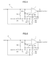
- FIG. 5 illustrates a circuit diagram of an offset reduction output circuit according to a first embodiment of the present invention
- FIG. 6 illustrates a circuit diagram showing on/off states of switch devices in a reset operation of the output circuit shown in FIG. 5 ;
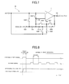
- FIG. 7 is a circuit diagram showing on/off states of switch devices in a normal output operation of the output circuit shown in FIG. 5 ;
- FIG. 8 is a timing chart among an external reset signal, a writing signal, and the voltage variation at a particular node in the output circuit of FIG. 5 ;
- FIG. 9 is a circuit diagram of an offset reduction output circuit according to a second embodiment of the present invention.
- FIG. 10 is a timing diagram showing the operations of two blocks in the output circuit shown in FIG. 9 ;
- FIG. 11 is a circuit diagram showing on/off states of switch devices when one block is in a reset condition and the other block is in a normal output mode in the circuit of FIG. 9 ;
- FIG. 12 is a circuit diagram showing on/off states of the switch devices when the other block is in the reset condition and said one block is in the normal output mode in the output circuit of FIG. 9 .
- the offset reduction output circuit 10 includes switch devices SW 7 and SW 8 in addition to the structure of the offset reduction output circuit 5 shown in FIG. 1 .
- the switch device SW 7 is connected to a switch device SW 4 in series.
- One terminal of the switch device SW 4 is connected to an inverting input terminal of an output amplifier 1
- an opposite terminal of the switch device SW 7 is connected to an output terminal OUT of the output amplifier 1 .
- the switch device SW 8 is connected between a connection point (node) FB 3 , which is provided between the switch device SW 4 and the switch device SW 7 , and an application terminal of a reference voltage VOP. Since other components of the output circuit 10 are similar to those shown in FIG. 1 , the details thereof will not be described here.
- the switch devices SW 1 to SW 8 constitute a switching circuit.
- Each switch device has a P-channel FET, and a channel between a source and a drain is turned on or turned off according to a control signal supplied to a gate of the P-channel FET.
- a power supply voltage VDD is applied to a base element (substrate or back gate) of the FET.
- the switch device SW 4 corresponds to a first switch device
- the switch device SW 7 corresponds to a second switch
- the switch device SW 8 corresponds to a third switch device.
- the power supply voltage VDD is 18V
- the reference voltage VOP is 3V
- a ground voltage VSS is 0V
- the voltage VDAC is in the range from 0V to 18V. It should be noted, however, that the present invention is not limited to these numerals.
- the offset reduction output circuit 10 Similar to the offset reduction output circuit 5 shown in FIG. 1 , the offset reduction output circuit 10 having the above-described structure performs a reset operation and a normal output operation.
- the reset operation is performed upon receiving an external reset signal in synchronization with a vertical synchronization signal of an image signal.
- the reset operation of the output circuit 10 will be described.
- the switch devices SW 1 , SW 5 , and SW 8 are turned off, and the switch devices SW 2 , SW 3 , SW 4 , SW 6 , and SW 7 are turned on. Therefore, the reference voltage VOP is applied to an opposite terminal of an input capacitor Cin through the switch device SW 2 while being applied to an opposite terminal of an output capacitor Cout through the switch device SW 6 . Since an inverting input terminal of the output amplifier 1 and a non-inverting input terminal of the output amplifier 1 are shorted with each other by the switch device SW 3 , an offset voltage ⁇ V is generated at the output terminal of the output amplifier 1 .
- the offset voltage ⁇ V is supplied to a node FB through the switch devices SW 7 and SW 4 . As a result, the offset voltage ⁇ V is charged in the input capacitor Cin and the output capacitor Cout. In this state, the operation of the offset reduction output circuit 10 is stabilized.
- the normal output operation will be described.
- the switch devices SW 1 , SW 5 , and SW 8 are turned on, and the switch devices SW 2 , SW 3 , SW 4 , SW 6 , and SW 7 are turned off as shown in FIG. 7 .
- the node FB of the inverting input terminal comes into a floating state, the output amplifier 1 is operated in such a manner that the voltage of the node FB is kept to the reference voltage VOP. In other words, charges flow in the input capacitor Cin corresponding to the differential voltage between the reference voltage VOP and the voltage VDAC, and charges flow in the output capacitor Cout corresponding to the differential voltage between the output voltage of the output amplifier 1 and the reference voltage VOP.
- the output voltage is generated from the output amplifier 1 with the offset voltage ⁇ V being canceled.
- the output voltage of the output amplifier 1 is supplied, as a driving voltage, to pixels of a liquid crystal display panel by those switching elements (not shown) which are turned on during a writing period in response to a writing signal in every one horizontal writing period.
- the reference voltage VOP is applied to the node FB 3 of the switch devices SW 4 and SW 7 through the switch device SW 8 , the voltage of the node FB 3 is held to the reference voltage VOP. Therefore, the voltage between both terminals of the switch device SW 4 , that is, the voltage between the source and the drain of the switch device SW 4 is equal to the reference voltage VOP, and a current leaking between the source and the drain of the switch device SW 4 is reduced. Also a current leaking from the output terminal OUT of the output amplifier 1 to the node FB through the channel between the source and the drain of the switch device SW 4 is reduced.
- the voltage at the node FB of the inverting input terminal of the output amplifier 1 is equal to the reference voltage VOP in response to the reset signal in the reset operation. Even if the normal output operation is performed after the reset operation, the voltage at the node FB is approximately maintained at the reference voltage VOP for a long time. In other words, since the leakage current can be reduced as described above, the reference voltage VOP at the node FB hardly drops. Accordingly, the offset voltage of the output amplifier 1 is cancelled in an appropriate matter, and the degradation of the display quality is prevented.
- FIG. 9 illustrates the structure of the offset reduction output circuit 12 according to a second embodiment of the present invention. Similar reference numerals and symbols are used in the first and second embodiments to designate similar elements and items.
- the offset reduction output circuit 12 includes a block A and a block B.
- the block A includes switch devices SW 3 , and SW 7 to SW 9 in addition to the structure of the offset reduction output circuit 5 shown in FIG. 1 .
- the input capacitor is designated by Cin 1 , not Cin, and may be referred to as a first input capacitor
- the output capacitor is designated by Cout 1 , not Cout, and may be referred to as a first output capacitor.
- the application terminal of the reference voltage VOP is connected to a non-inverting input terminal of the output amplifier 1 , and the switch device SW 1 is connected between the application terminal of the voltage VDAC and an opposite terminal of the input Capacitor Cin 1 .
- the switch device SW 2 is connected between the application terminal of the reference voltage VOP and the opposite terminal of the input capacitor Cin 1 .
- the switch device SW 3 is connected between the application terminal of the reference voltage VOP and one terminal of the input capacitor Cin 1 , that is, a node FB 1 .
- the node FB 1 is connected to one terminal of the output capacitor Cout 1 .
- the switch device SW 4 is connected to the switch device SW 9 in series.
- One terminal of the switch device SW 4 is connected to the node FB 1 , and the opposite terminal of the switch device SW 9 is connected to the output terminal OUT of the output amplifier 1 .
- the switch device SW 5 is connected between an opposite terminal of the output capacitor Cout 1 and a node which is provided between the switch device SW 4 and the switch device SW 9 .
- the switch device SW 6 is connected between the opposite terminal of the output capacitor Cout 1 and the application terminal of the reference voltage VOP.
- the switch device SW 7 is connected between the node FB of the inverting input terminal of the output amplifier 1 and the node FB 1 .
- the switch device S 8 is connected between the application terminal of the reference voltage VOP and the node between the switch device SW 4 and the switch device SW 9 .
- the block B includes switch devices SW 10 to SW 18 , an input capacitor Cin 2 (second input capacitor), and an output capacitor Cout 2 (second output capacitor). Other components of the block B are the same as those of the block A except for the output amplifier 1 . Regarding the relation between components of the blocks A and B, the input capacitor Cin 2 corresponds to the input capacitor Cin 1 , and the output capacitor Cout 2 corresponds to the output capacitor Cout 1 .
- the switch device SW 10 corresponds to the switch device SW 1 , the switch device SW 11 corresponds to the switch device SW 2 , and the switch device SW 12 corresponds to the switch device SW 3 . Since other components of the block B correspond to other components of block A in order of reference numerals, the description thereof will be omitted.
- the opposite terminal of the input capacitor Cin 2 is connected to a node FB 2 .
- the block A may be referred to as a first block, and the block B may be referred to as a second block.
- the switch device SW 13 may be referred to as the fourth switch device, the switch device SW 18 may be referred to as the fifth switch device, and the switch device SW 17 may be referred to as the sixth switch device.
- the block A and the block B of the output circuit 12 alternately repeat the normal output operation and the reset operation in response to the writing signal in every one horizontal writing period.
- the block B performs the reset operation.
- the block B performs the normal output operation.
- the block A may perform the reset operation in response to the external reset signal and then performs the normal output operation in response to an initial writing signal.
- the block B performs the reset operation in response to the initial writing signal. Thereafter, the blocks A and B perform the reset operation and the normal output operation as shown in FIG. 10 .
- the switch devices SW 1 , SW 5 , SW 7 , and SW 9 in the block A are turned on, and the switch devices SW 2 to SW 4 , SW 6 , and SW 8 in the block A are turned off as shown in FIG. 11 .
- the switch devices SW 10 , SW 14 , SW 16 , and SW 18 are turned off, and the switch devices SW 11 to SW 13 , SW 15 , and SW 17 are turned on.
- the switch devices SW 1 , SW 5 , SW 7 , and SW 9 are turned off and the switch devices SW 2 to SW 4 , SW 6 , and SW 8 are turned on in the block A as shown in FIG. 12 .
- the switch devices SW 10 , SW 14 , SW 16 , and SW 18 are turned on, and the switch devices SW 11 to SW 13 , SW 15 , and SW 17 are turned off.
- the block A enters the reset mode in response to the external reset signal and then shifts to the normal output operation in response to the initial writing signal.
- the block B performs the reset operation in response to the initial writing signal. Thereafter, the blocks A and B perform the reset operation and the normal output operation as shown in FIG. 10 .
- the switch devices SW 2 to SW 4 , SW 6 , and SW 8 are turned on so that both terminals of the input capacitor Cin 1 are shorted and both terminals of the output capacitor Cout 1 are shorted while the reference voltage VOP is being applied.
- the reference voltage VOP is applied to both terminals of each of the input and output capacitors Cin 1 and Cout 1 .
- the voltage of the node FB 1 becomes equal to the reference voltage VOP.
- the node FB 1 is electrically disconnected from the inverting input terminal of the output amplifier 1 due to the turning off of the switch device SW 7 , and the output terminal OUT of the output amplifier 1 is independent from other circuit parts (except for the resistor R 1 ) of the block A due to the turning off of the switch device SW 9 .
- the node FB 1 becomes in a floating state, and the output amplifier 1 is operated such that the voltage of the node FB 1 is held to the reference voltage VOP.
- the input capacitor Cin 1 corresponding to the differential voltage between the reference voltage VOP and the voltage VDAC
- the output capacitor Cout 1 corresponding to the differential voltage between the output voltage of the output amplifier 1 and the reference voltage VOP, thereby generating the output voltage.
- the block B When the block A performs the normal output operation, the block B is in the reset condition.
- the switch devices SW 11 to SW 13 , SW 15 , and SW 17 are turned on, so that both terminals of the input capacitor Cin 2 are shorted and both terminals of the output capacitor Cout 2 are shorted while the reference voltage VOP is being applied.
- the reference voltage VOP is applied to both terminals of each of the input and output capacitors Cin 2 and Cou 2 .
- the voltage of the node FB 2 becomes equal to the reference voltage VOP.
- the node FB 2 When the block B is in the reset condition, the node FB 2 is electrically disconnected from the inverting input terminal of the output amplifier 1 due to the turning off of the switch SW 16 .
- the output terminal OUT of the output amplifier 1 becomes independent from other circuit parts of the block B due to the turning off of the switch S 18 .
- the node FB 2 When the block B shifts to the normal output operation from the reset condition, the node FB 2 also shifts to a floating state, and the output amplifier 1 is operated such that the voltage of the connection point FB 2 is kept to the reference voltage VOP.
- the input capacitor Cin 2 corresponding to the differential voltage between the reference voltage VOP and the voltage VDAC
- the output capacitor Cout 2 corresponding to the differential voltage between the output voltage of the output amplifier 1 and the reference voltage VOP
- the block A When the block B performs the normal output operation, the block A is in the reset condition as described above.
- the reference voltage VOP is applied to the node FB 3 between the switch device SW 4 and the switch device SW 9 through the switch device SW 8 , the voltage of the connection point FB 3 is held to the reference voltage VOP. Therefore, the voltage between both terminals of the switch device SW 4 , that is, the voltage between the source and the drain of the switch device SW 4 , is equal to the reference voltage VOP, and the leakage current between the source and drain of the switch device SW 4 is reduced (eliminated). Also the current leaking from the output terminal OUT of the output amplifier 1 to the node FB through the channel between the source and drain of the switch device SW 4 is reduced.
- the reference voltage VOP is applied to the node FB 4 between the switch device SW 13 and the switch device SW 18 through the switch device SW 17 , the voltage of the connection point FB 4 is held to the reference voltage VOP. Therefore, the voltage between both terminals of the switch device SW 13 , that is, the voltage between the source and the drain, is equal to the reference voltage VOP, and the leakage current leaking between the source and drain of the switch device SW 13 can be reduced. Also the current leaking from the output terminal OUT of the output amplifier 1 to the node FB through the channel between the source and drain of the switch device SW 13 can be reduced.
- the blocks A and B alternately repeat the normal output operation and the reset operation at the timings in synchronization with the horizontal synchronization signals in such a manner that an operation of the block A differs from an operation of the block B, the reference voltage which is changed due to the leakage current can return to an original reference voltage in every one horizontal period. Accordingly, the same quantity as a leaking current to the basis parts from the switch devices (FETs) can be supplemented (compensated), and the influence of the offset voltage of the output amplifier can be more effectively minimized.
- FETs switch devices
- the present invention is not limited to the illustrated embodiments.
- the block A includes the output amplifier 1 in the offset reduction output circuit 12 shown in FIG. 9
- the output amplifier 1 may be provided in the block B, or provided outside the block A (or B).
- the switch device may not be limited to the P-channel FET, but may be an N-channel FET.
Landscapes
- Engineering & Computer Science (AREA)
- Chemical & Material Sciences (AREA)
- Crystallography & Structural Chemistry (AREA)
- Physics & Mathematics (AREA)
- Computer Hardware Design (AREA)
- General Physics & Mathematics (AREA)
- Theoretical Computer Science (AREA)
- Liquid Crystal Display Device Control (AREA)
- Amplifiers (AREA)
- Liquid Crystal (AREA)
- Control Of Indicators Other Than Cathode Ray Tubes (AREA)
- Analogue/Digital Conversion (AREA)
Abstract
Description
- The present invention relates to an offset-reducing output circuit of a source driver adapted to drive a liquid crystal device.
- A source driver to drive a liquid crystal panel is equipped with a function of canceling an offset component of a driving voltage issued from an output circuit including an operational amplifier. Such source drivers are, for example, disclosed in Japanese Patent Application Publication (Kokai) No. 11-044872 and Japanese Patent Application Publication (Kokai) No. 2001-67047.
FIG. 1 of the accompanying drawings is a circuit diagram showing the structure of an output circuit for reducing an offset of a source driver in Japanese Patent Application Publication No. 2001-67047. The offset-reducingoutput circuit 5 is a capacitor-coupled operational amplifier, and includes anoutput amplifier 1, an input capacitor Cin, an output capacitor Cout, switch devices SW1 to SW6, and a resistor R1. A reference voltage VOP and a voltage VDAC are supplied to the offset-reducingoutput circuit 5 as input voltages. The voltage VDAC is a voltage (gray-scale voltage) obtained by converting digital data representing the gray scale of each pixel supplied to a source driver into an analog voltage by a D/A (digital/analog) converter (not shown) provided in the source driver. An application terminal of the reference voltage VOP is connected to a non-inverting input terminal of the output amplifier (operational amplifier) 1. An inverting input terminal of theoutput amplifier 1 is connected to one terminal of the input capacitor Cin and also connected to one terminal of the output capacitor Cout. The switch device SW1 is connected between an application terminal of the voltage VDAC and an opposite terminal of the input capacitor Cin. The switch device SW2 is connected between the application terminal of the reference voltage VOP and the opposite terminal of the input capacitor Cin. The switch device SW3 is connected between the non-inverting input terminal and the inverting input terminal of theoutput amplifier 1. The switch device SW4 is connected between the inverting input terminal of theoutput amplifier 1 and an output terminal OUT of theoutput amplifier 1. The switch device SW5 is connected between an opposite terminal of the output capacitor Cout and the output terminal OUT of theoutput amplifier 1. The switch device SW6 is connected between the opposite terminal of the output capacitor Cout and the application terminal of the reference voltage VOP. One terminal of the resistor R1 is connected to the output terminal OUT of theoutput amplifier 1, so that an output voltage of theoutput amplifier 1 is issued, as a driving voltage, from a terminal PAD through the resistor R1. - The offset-reducing
output circuit 5 ofFIG. 1 has a reset operation and a normal output operation. The reset operation is triggered upon receiving an external reset signal in synchronization with a vertical synchronization signal of an image signal. The voltage VDAC is generated in synchronization with a horizontal synchronization signal during the normal output operation. - Referring now to
FIG. 2 of the accompanying drawings, the reset operation of theoutput circuit 5 will be described. In the reset operation, the switch devices SW1 and SW5 are turned off, and the switch devices SW2, SW3, SW4, and SW6 are turned on. As a result, voltages at all connection points (nodes), expressed as black dots inFIG. 2 , become equal to the reference voltage VOP. This is the reset operation. In other words, the reference voltage VOP is applied to the opposite terminal of the input capacitor Cin through the switch device SW2 while being applied to an opposite terminal of the output capacitor Cout through the switch device SW6. Since the inverting input terminal and the non-inverting input terminal of theoutput amplifier 1 are shorted with each other by the switch device SW3, an offset voltage ΔV is generated at the output terminal of theoutput amplifier 1. The offset voltage ΔV is supplied to a node FB through the switch device SW4. Accordingly, the offset voltage ΔV is charged or accumulated in the input capacitor Cin and the output capacitor Cout. In this state, the operation of the offsetreduction output circuit 5 is stabilized. - Referring now to
FIG. 3 , the normal output operation of theoutput circuit 5 will be described. When the operation mode changes to the normal output operation from the reset operation, the switch devices SW1 and SW5 are turned on, and the switch devices SW2, SW3, SW4, and SW6 are turned off as shown inFIG. 3 . The node FB of the inverting input terminal comes into a floating state, and theoutput amplifier 1 is operated in such a manner that the voltage of the node FB stays at the reference voltage VOP. In other words, charges flow in the input capacitor Cin corresponding to the voltage difference between the reference voltage VOP and the voltage VDAC, and charges flow in the output capacitor Cout corresponding to the voltage difference between the output voltage of theoutput amplifier 1 and the reference voltage VOP. Therefore, an output voltage is generated from theoutput amplifier 1 with the offset voltage ΔV being cancelled. Since a voltage corresponding to the voltage VDAC is applied to the inverting input terminal through the input capacitor Cin, a voltage corresponding to a differential voltage between the reference voltage VOP and a voltage of the inverting input terminal is generated. In the normal output operation, the output voltage of theoutput amplifier 1 is supplied, as a driving voltage, to pixels of a liquid crystal display panel during a writing period in response to a writing signal in every one horizontal writing period. - Referring now to
FIG. 4 , the operation of the offsetreduction output circuit 5 shown inFIG. 1 will be further discussed. As described earlier, theoutput circuit 5 generates the reset and writing signals. In the reset operation, the voltage at the node FB of the inverting input terminal of theoutput amplifier 1 approximates the reference voltage VOP (including offset voltage ΔV) in response to the reset signal. If the normal output operation is performed after the reset operation, the voltage of the node FB gradually decreases from the reference voltage VOP. This phenomenon occurs due to the leakage current flowing to a base element (substrate) of the switch device SW4 including a field-effect transistor (FET), and/or the leakage current between a source and a drain of the switch device SW4. Accordingly, it is difficult to maintain the reference voltage VOP at the node FB of the inverting input terminal of theoutput amplifier 1 for a long time, and therefore an offset voltage in the output voltage of theoutput amplifier 1 increases to degrade display quality of the liquid crystal display panel. - An object of the present invention is to provide an offset reduction output circuit used for a source driver of a liquid crystal device, capable of preventing display quality degradation by properly reducing an offset voltage of an output amplifier.
- According to one aspect of the present invention, there is provided an offset reduction output circuit of a source driver for receiving a gray scale voltage corresponding to gray scales represented by digital data and for generating a driving voltage to a liquid display panel. The offset reduction output circuit includes an operational amplifier having a non-inverting input terminal to receive a reference voltage. The offset reduction output circuit also a first input capacitor and a first output capacitor. One terminal of the first input capacitor and one terminal of the first output capacitor are connected to a first node connected to an inverting input terminal of the operational amplifier in at least a normal output operation. The offset reduction output circuit also includes a first switching circuit to short both terminals of the first input capacitor and short both terminals of the first output capacitor in a reset operation so that the reference voltage is applied to the terminals of the first input and output capacitors. The first switching circuit is also adapted to apply the gray scale voltage to an opposite terminal of the first input capacitor and connect an opposite terminal of the first output capacitor to an output terminal of the operational amplifier in the normal output operation after the reset operation. The first switching circuit has first and second switch devices connected with each other in series at a predetermined connection point. The first and second switch devices are connected between the first node and the output terminal of the operational amplifier. The first and second switch devices are turned on in the reset operation, and turned off in the normal output operation. The reference voltage is applied to the predetermined connection point of the first and second switch devices in the normal output operation.
- Since the reference voltage is applied to the in-series connection point (predetermined connection point) of the first and second switch devices in the normal output operation of the offset reduction output circuit, the voltage at the in-series connection point is fixed to the reference voltage. Therefore, a voltage between the two terminals (for example, voltage between the source and the drain) of the first switch device provided on the first node side becomes equal to the reference voltage. Thus, the leakage current between the both terminals of the first switch device can be reduced. In addition, the current leaking from the output terminal of the operational amplifier to the first node through the both terminals of the first switch device can be reduced. Consequently, the offset voltage of the operational amplifier can be properly reduced, so that the degradation of the display quality can be prevented.
- These and other objects, aspects and advantages of the present invention will become apparent to those skilled in the art from the following detailed description when read and understood in conjunction with the appended claims and drawings.
-
FIG. 1 shows a circuit diagram of an offset reduction output circuit according to the related art; -
FIG. 2 is a circuit diagram showing on/off states of switch devices in the output circuit shown inFIG. 1 during a reset operation; -
FIG. 3 is a circuit diagram showing on/off states of the switch devices in the output circuit ofFIG. 1 during a normal output operation; -
FIG. 4 depicts a timing chart among an external reset signal, a writing signal, and the voltage variation at a particular node in the output circuit ofFIG. 1 ; -
FIG. 5 illustrates a circuit diagram of an offset reduction output circuit according to a first embodiment of the present invention; -
FIG. 6 illustrates a circuit diagram showing on/off states of switch devices in a reset operation of the output circuit shown inFIG. 5 ; -
FIG. 7 is a circuit diagram showing on/off states of switch devices in a normal output operation of the output circuit shown inFIG. 5 ; -
FIG. 8 is a timing chart among an external reset signal, a writing signal, and the voltage variation at a particular node in the output circuit ofFIG. 5 ; -
FIG. 9 is a circuit diagram of an offset reduction output circuit according to a second embodiment of the present invention; -
FIG. 10 is a timing diagram showing the operations of two blocks in the output circuit shown inFIG. 9 ; -
FIG. 11 is a circuit diagram showing on/off states of switch devices when one block is in a reset condition and the other block is in a normal output mode in the circuit ofFIG. 9 ; and -
FIG. 12 is a circuit diagram showing on/off states of the switch devices when the other block is in the reset condition and said one block is in the normal output mode in the output circuit ofFIG. 9 . - Exemplary embodiments of the present invention will be described with reference to
FIG. 5 toFIG. 12 of the accompanying drawings. Like reference numerals and symbols are used to designate like elements and items in different drawings. - Referring to
FIG. 5 , the structure of an offsetreduction output circuit 10 according to a first embodiment of the present invention will be described. The offsetreduction output circuit 10 includes switch devices SW7 and SW8 in addition to the structure of the offsetreduction output circuit 5 shown inFIG. 1 . The switch device SW7 is connected to a switch device SW4 in series. One terminal of the switch device SW4 is connected to an inverting input terminal of anoutput amplifier 1, and an opposite terminal of the switch device SW7 is connected to an output terminal OUT of theoutput amplifier 1. The switch device SW8 is connected between a connection point (node) FB3, which is provided between the switch device SW4 and the switch device SW7, and an application terminal of a reference voltage VOP. Since other components of theoutput circuit 10 are similar to those shown inFIG. 1 , the details thereof will not be described here. - The switch devices SW1 to SW8 constitute a switching circuit. Each switch device has a P-channel FET, and a channel between a source and a drain is turned on or turned off according to a control signal supplied to a gate of the P-channel FET. A power supply voltage VDD is applied to a base element (substrate or back gate) of the FET. The switch device SW4 corresponds to a first switch device, the switch device SW7 corresponds to a second switch, and the switch device SW8 corresponds to a third switch device.
- In this embodiment, the power supply voltage VDD is 18V, the reference voltage VOP is 3V, a ground voltage VSS is 0V, and the voltage VDAC is in the range from 0V to 18V. It should be noted, however, that the present invention is not limited to these numerals.
- Similar to the offset
reduction output circuit 5 shown inFIG. 1 , the offsetreduction output circuit 10 having the above-described structure performs a reset operation and a normal output operation. The reset operation is performed upon receiving an external reset signal in synchronization with a vertical synchronization signal of an image signal. - Referring to
FIG. 6 , the reset operation of theoutput circuit 10 will be described. In the reset operation, the switch devices SW1, SW5, and SW8 are turned off, and the switch devices SW2, SW3, SW4, SW6, and SW7 are turned on. Therefore, the reference voltage VOP is applied to an opposite terminal of an input capacitor Cin through the switch device SW2 while being applied to an opposite terminal of an output capacitor Cout through the switch device SW6. Since an inverting input terminal of theoutput amplifier 1 and a non-inverting input terminal of theoutput amplifier 1 are shorted with each other by the switch device SW3, an offset voltage ΔV is generated at the output terminal of theoutput amplifier 1. The offset voltage ΔV is supplied to a node FB through the switch devices SW7 and SW4. As a result, the offset voltage ΔV is charged in the input capacitor Cin and the output capacitor Cout. In this state, the operation of the offsetreduction output circuit 10 is stabilized. - Referring to
FIG. 7 , the normal output operation will be described. When a normal output operation is performed after the reset operation, the switch devices SW1, SW5, and SW8 are turned on, and the switch devices SW2, SW3, SW4, SW6, and SW7 are turned off as shown inFIG. 7 . The node FB of the inverting input terminal comes into a floating state, theoutput amplifier 1 is operated in such a manner that the voltage of the node FB is kept to the reference voltage VOP. In other words, charges flow in the input capacitor Cin corresponding to the differential voltage between the reference voltage VOP and the voltage VDAC, and charges flow in the output capacitor Cout corresponding to the differential voltage between the output voltage of theoutput amplifier 1 and the reference voltage VOP. Therefore, the output voltage is generated from theoutput amplifier 1 with the offset voltage ΔV being canceled. In the normal output operation, the output voltage of theoutput amplifier 1 is supplied, as a driving voltage, to pixels of a liquid crystal display panel by those switching elements (not shown) which are turned on during a writing period in response to a writing signal in every one horizontal writing period. - Since the reference voltage VOP is applied to the node FB3 of the switch devices SW4 and SW7 through the switch device SW8, the voltage of the node FB3 is held to the reference voltage VOP. Therefore, the voltage between both terminals of the switch device SW4, that is, the voltage between the source and the drain of the switch device SW4 is equal to the reference voltage VOP, and a current leaking between the source and the drain of the switch device SW4 is reduced. Also a current leaking from the output terminal OUT of the
output amplifier 1 to the node FB through the channel between the source and the drain of the switch device SW4 is reduced. - Therefore, as shown in
FIG. 8 , the voltage at the node FB of the inverting input terminal of theoutput amplifier 1 is equal to the reference voltage VOP in response to the reset signal in the reset operation. Even if the normal output operation is performed after the reset operation, the voltage at the node FB is approximately maintained at the reference voltage VOP for a long time. In other words, since the leakage current can be reduced as described above, the reference voltage VOP at the node FB hardly drops. Accordingly, the offset voltage of theoutput amplifier 1 is cancelled in an appropriate matter, and the degradation of the display quality is prevented. -
FIG. 9 illustrates the structure of the offsetreduction output circuit 12 according to a second embodiment of the present invention. Similar reference numerals and symbols are used in the first and second embodiments to designate similar elements and items. The offsetreduction output circuit 12 includes a block A and a block B. The block A includes switch devices SW3, and SW7 to SW9 in addition to the structure of the offsetreduction output circuit 5 shown inFIG. 1 . In the second embodiment, the input capacitor is designated by Cin1, not Cin, and may be referred to as a first input capacitor, and the output capacitor is designated by Cout1, not Cout, and may be referred to as a first output capacitor. The application terminal of the reference voltage VOP is connected to a non-inverting input terminal of theoutput amplifier 1, and the switch device SW1 is connected between the application terminal of the voltage VDAC and an opposite terminal of the input Capacitor Cin1. The switch device SW2 is connected between the application terminal of the reference voltage VOP and the opposite terminal of the input capacitor Cin1. The switch device SW3 is connected between the application terminal of the reference voltage VOP and one terminal of the input capacitor Cin1, that is, a node FB1. The node FB1 is connected to one terminal of the output capacitor Cout1. The switch device SW4 is connected to the switch device SW9 in series. One terminal of the switch device SW4 is connected to the node FB1, and the opposite terminal of the switch device SW9 is connected to the output terminal OUT of theoutput amplifier 1. The switch device SW5 is connected between an opposite terminal of the output capacitor Cout1 and a node which is provided between the switch device SW4 and the switch device SW9. The switch device SW6 is connected between the opposite terminal of the output capacitor Cout1 and the application terminal of the reference voltage VOP. The switch device SW7 is connected between the node FB of the inverting input terminal of theoutput amplifier 1 and the node FB1. The switch device S8 is connected between the application terminal of the reference voltage VOP and the node between the switch device SW4 and the switch device SW9. - The block B includes switch devices SW10 to SW18, an input capacitor Cin2 (second input capacitor), and an output capacitor Cout2 (second output capacitor). Other components of the block B are the same as those of the block A except for the
output amplifier 1. Regarding the relation between components of the blocks A and B, the input capacitor Cin2 corresponds to the input capacitor Cin1, and the output capacitor Cout2 corresponds to the output capacitor Cout1. The switch device SW10 corresponds to the switch device SW1, the switch device SW11 corresponds to the switch device SW2, and the switch device SW12 corresponds to the switch device SW3. Since other components of the block B correspond to other components of block A in order of reference numerals, the description thereof will be omitted. The opposite terminal of the input capacitor Cin2 is connected to a node FB2. - The block A may be referred to as a first block, and the block B may be referred to as a second block. The switch device SW13 may be referred to as the fourth switch device, the switch device SW18 may be referred to as the fifth switch device, and the switch device SW17 may be referred to as the sixth switch device.
- Referring to
FIG. 10 , the block A and the block B of theoutput circuit 12 alternately repeat the normal output operation and the reset operation in response to the writing signal in every one horizontal writing period. When the block A performs the normal output operation, the block B performs the reset operation. When the block A performs the reset operation, the block B performs the normal output operation. - For example, at the beginning of each frame, the block A may perform the reset operation in response to the external reset signal and then performs the normal output operation in response to an initial writing signal. The block B performs the reset operation in response to the initial writing signal. Thereafter, the blocks A and B perform the reset operation and the normal output operation as shown in
FIG. 10 . - When the block A is in the normal output mode and the block B is in the reset mode, the switch devices SW1, SW5, SW7, and SW9 in the block A are turned on, and the switch devices SW2 to SW4, SW6, and SW8 in the block A are turned off as shown in
FIG. 11 . In the block B, the switch devices SW10, SW14, SW16, and SW18 are turned off, and the switch devices SW11 to SW13, SW15, and SW17 are turned on. - When the block A is in the reset mode and the block B is in the normal output mode, then the switch devices SW1, SW5, SW7, and SW9 are turned off and the switch devices SW2 to SW4, SW6, and SW8 are turned on in the block A as shown in
FIG. 12 . In the block B, the switch devices SW10, SW14, SW16, and SW18 are turned on, and the switch devices SW11 to SW13, SW15, and SW17 are turned off. - For example, at the beginning of each frame, the block A enters the reset mode in response to the external reset signal and then shifts to the normal output operation in response to the initial writing signal. The block B performs the reset operation in response to the initial writing signal. Thereafter, the blocks A and B perform the reset operation and the normal output operation as shown in
FIG. 10 . - In the reset operation of the block A, the switch devices SW2 to SW4, SW6, and SW8 are turned on so that both terminals of the input capacitor Cin1 are shorted and both terminals of the output capacitor Cout1 are shorted while the reference voltage VOP is being applied. As such, the reference voltage VOP is applied to both terminals of each of the input and output capacitors Cin1 and Cout1. The voltage of the node FB1 becomes equal to the reference voltage VOP. In addition, in the reset operation of the block A, the node FB1 is electrically disconnected from the inverting input terminal of the
output amplifier 1 due to the turning off of the switch device SW7, and the output terminal OUT of theoutput amplifier 1 is independent from other circuit parts (except for the resistor R1) of the block A due to the turning off of the switch device SW9. - When the block A enters the normal output operation from the reset condition, the node FB1 becomes in a floating state, and the
output amplifier 1 is operated such that the voltage of the node FB1 is held to the reference voltage VOP. In other words, charges flow in the input capacitor Cin1 corresponding to the differential voltage between the reference voltage VOP and the voltage VDAC, and charges flow in the output capacitor Cout1 corresponding to the differential voltage between the output voltage of theoutput amplifier 1 and the reference voltage VOP, thereby generating the output voltage. - When the block A performs the normal output operation, the block B is in the reset condition. When the block B is in the reset condition, the switch devices SW11 to SW13, SW15, and SW17 are turned on, so that both terminals of the input capacitor Cin2 are shorted and both terminals of the output capacitor Cout2 are shorted while the reference voltage VOP is being applied. Thus the reference voltage VOP is applied to both terminals of each of the input and output capacitors Cin2 and Cou2. The voltage of the node FB2 becomes equal to the reference voltage VOP. When the block B is in the reset condition, the node FB2 is electrically disconnected from the inverting input terminal of the
output amplifier 1 due to the turning off of the switch SW16. In addition, the output terminal OUT of theoutput amplifier 1 becomes independent from other circuit parts of the block B due to the turning off of the switch S18. - When the block B shifts to the normal output operation from the reset condition, the node FB2 also shifts to a floating state, and the
output amplifier 1 is operated such that the voltage of the connection point FB2 is kept to the reference voltage VOP. In other words, charges flow in the input capacitor Cin2 corresponding to the differential voltage between the reference voltage VOP and the voltage VDAC, and charges flow in the output capacitor Cout2 corresponding to the differential voltage between the output voltage of theoutput amplifier 1 and the reference voltage VOP, thereby generating the output voltage. - When the block B performs the normal output operation, the block A is in the reset condition as described above.
- In the block A, since the reference voltage VOP is applied to the node FB3 between the switch device SW4 and the switch device SW9 through the switch device SW8, the voltage of the connection point FB3 is held to the reference voltage VOP. Therefore, the voltage between both terminals of the switch device SW4, that is, the voltage between the source and the drain of the switch device SW4, is equal to the reference voltage VOP, and the leakage current between the source and drain of the switch device SW4 is reduced (eliminated). Also the current leaking from the output terminal OUT of the
output amplifier 1 to the node FB through the channel between the source and drain of the switch device SW4 is reduced. - Similarly, in the block B, since the reference voltage VOP is applied to the node FB4 between the switch device SW13 and the switch device SW18 through the switch device SW17, the voltage of the connection point FB4 is held to the reference voltage VOP. Therefore, the voltage between both terminals of the switch device SW13, that is, the voltage between the source and the drain, is equal to the reference voltage VOP, and the leakage current leaking between the source and drain of the switch device SW13 can be reduced. Also the current leaking from the output terminal OUT of the
output amplifier 1 to the node FB through the channel between the source and drain of the switch device SW13 can be reduced. - Since the blocks A and B alternately repeat the normal output operation and the reset operation at the timings in synchronization with the horizontal synchronization signals in such a manner that an operation of the block A differs from an operation of the block B, the reference voltage which is changed due to the leakage current can return to an original reference voltage in every one horizontal period. Accordingly, the same quantity as a leaking current to the basis parts from the switch devices (FETs) can be supplemented (compensated), and the influence of the offset voltage of the output amplifier can be more effectively minimized.
- It should be noted that the present invention is not limited to the illustrated embodiments. For example, although the block A includes the
output amplifier 1 in the offsetreduction output circuit 12 shown inFIG. 9 , theoutput amplifier 1 may be provided in the block B, or provided outside the block A (or B). In addition, the switch device may not be limited to the P-channel FET, but may be an N-channel FET. - This application is based on Japanese Patent Application No. 2011-78010 filed on Mar. 31, 2011, and the entire disclosure thereof is incorporated herein by reference.
Claims (9)
Applications Claiming Priority (2)
| Application Number | Priority Date | Filing Date | Title |
|---|---|---|---|
| JP2011078010A JP5738041B2 (en) | 2011-03-31 | 2011-03-31 | Source driver offset reduction output circuit for liquid crystal drive |
| JP2011-078010 | 2011-03-31 |
Publications (2)
| Publication Number | Publication Date |
|---|---|
| US20120249607A1 true US20120249607A1 (en) | 2012-10-04 |
| US8736642B2 US8736642B2 (en) | 2014-05-27 |
Family
ID=46926624
Family Applications (1)
| Application Number | Title | Priority Date | Filing Date |
|---|---|---|---|
| US13/418,719 Active 2032-11-21 US8736642B2 (en) | 2011-03-31 | 2012-03-13 | Output circuit for reducing offset for use in source driver adapted to drive liquid crystal device |
Country Status (2)
| Country | Link |
|---|---|
| US (1) | US8736642B2 (en) |
| JP (1) | JP5738041B2 (en) |
Cited By (3)
| Publication number | Priority date | Publication date | Assignee | Title |
|---|---|---|---|---|
| US20170193959A1 (en) * | 2015-12-31 | 2017-07-06 | Samsung Display Co., Ltd. | Display apparatus and method of operating the same |
| US20170263205A1 (en) * | 2016-03-09 | 2017-09-14 | Semiconductor Energy Laboratory Co., Ltd. | Semiconductor device, display device, and electronic device |
| US10043454B2 (en) | 2014-09-12 | 2018-08-07 | Joled Inc. | Source driver circuit, and display device |
Families Citing this family (1)
| Publication number | Priority date | Publication date | Assignee | Title |
|---|---|---|---|---|
| KR102931037B1 (en) | 2022-03-29 | 2026-02-24 | 삼성전자주식회사 | Semiconductor device |
Citations (2)
| Publication number | Priority date | Publication date | Assignee | Title |
|---|---|---|---|---|
| US20090278868A1 (en) * | 2002-02-06 | 2009-11-12 | Nec Corporation | Driving circuit for display apparatus, and method for controlling same |
| US20110187757A1 (en) * | 2010-01-29 | 2011-08-04 | Novatek Microelectronics Corp. | Source driving apparatus for display |
Family Cites Families (5)
| Publication number | Priority date | Publication date | Assignee | Title |
|---|---|---|---|---|
| JPH09146500A (en) * | 1995-11-22 | 1997-06-06 | Fujitsu Ltd | Voltage follower circuit, sample hold circuit using the same, and flat panel display device |
| JP3097612B2 (en) | 1997-07-25 | 2000-10-10 | 日本電気株式会社 | Liquid crystal drive semiconductor device |
| JP3897900B2 (en) * | 1998-04-13 | 2007-03-28 | 日本テキサス・インスツルメンツ株式会社 | Digital / analog conversion circuit |
| JP4510955B2 (en) | 1999-08-30 | 2010-07-28 | 日本テキサス・インスツルメンツ株式会社 | Data line drive circuit for liquid crystal display |
| JP2006324847A (en) * | 2005-05-18 | 2006-11-30 | Sony Corp | Sample hold circuit, serial / parallel conversion circuit, and display drive device |
-
2011
- 2011-03-31 JP JP2011078010A patent/JP5738041B2/en not_active Expired - Fee Related
-
2012
- 2012-03-13 US US13/418,719 patent/US8736642B2/en active Active
Patent Citations (2)
| Publication number | Priority date | Publication date | Assignee | Title |
|---|---|---|---|---|
| US20090278868A1 (en) * | 2002-02-06 | 2009-11-12 | Nec Corporation | Driving circuit for display apparatus, and method for controlling same |
| US20110187757A1 (en) * | 2010-01-29 | 2011-08-04 | Novatek Microelectronics Corp. | Source driving apparatus for display |
Cited By (6)
| Publication number | Priority date | Publication date | Assignee | Title |
|---|---|---|---|---|
| US10043454B2 (en) | 2014-09-12 | 2018-08-07 | Joled Inc. | Source driver circuit, and display device |
| US20170193959A1 (en) * | 2015-12-31 | 2017-07-06 | Samsung Display Co., Ltd. | Display apparatus and method of operating the same |
| US10152942B2 (en) * | 2015-12-31 | 2018-12-11 | Samsung Display Co., Ltd. | Display apparatus and method of operating the same |
| US20170263205A1 (en) * | 2016-03-09 | 2017-09-14 | Semiconductor Energy Laboratory Co., Ltd. | Semiconductor device, display device, and electronic device |
| US10083668B2 (en) * | 2016-03-09 | 2018-09-25 | Semiconductor Energy Laboratory Co., Ltd. | Semiconductor device, display device, and electronic device |
| US10832626B2 (en) | 2016-03-09 | 2020-11-10 | Semiconductor Energy Laboratory Co., Ltd. | Semiconductor device, display device, and electronic device |
Also Published As
| Publication number | Publication date |
|---|---|
| JP2012212046A (en) | 2012-11-01 |
| US8736642B2 (en) | 2014-05-27 |
| JP5738041B2 (en) | 2015-06-17 |
Similar Documents
| Publication | Publication Date | Title |
|---|---|---|
| US7358946B2 (en) | Offset cancel circuit of voltage follower equipped with operational amplifier | |
| US8531376B2 (en) | Bootstrap circuit, and shift register, scanning circuit, display device using the same | |
| US20100156474A1 (en) | Gate drive circuit and display apparatus having the same | |
| GB2385221A (en) | Amplifier offset reduction in an LCD or EL display grey-level driver circuit | |
| US7944439B2 (en) | Display device | |
| US8477159B2 (en) | Offset cancel output circuit of source driver for driving liquid crystal display | |
| US10839750B2 (en) | Electrostatic discharging circuit and display device including the same | |
| US20120032939A1 (en) | Output circuit, data driver and display device | |
| US20070176675A1 (en) | Differential amplifier and digital-to-analog converter | |
| US7414601B2 (en) | Driving circuit for liquid crystal display device and method of driving the same | |
| US7786970B2 (en) | Driver circuit of display device | |
| US8736642B2 (en) | Output circuit for reducing offset for use in source driver adapted to drive liquid crystal device | |
| US6812768B2 (en) | Input circuit, display device and information display apparatus | |
| US20120007901A1 (en) | Pixel circuitry of display device | |
| KR20080011896A (en) | Gate-on voltage generator circuit and gate-off voltage generator circuit and liquid crystal display device having them | |
| US20070052874A1 (en) | Display apparatus including sensor in pixel | |
| CN101154365A (en) | Drive circuits, optoelectronic devices and electronic equipment | |
| US8179359B2 (en) | Analog buffer circuit capable of compensating threshold voltage variation of transistor | |
| US20090167666A1 (en) | LCD Driver IC and Method for Operating the Same | |
| JP4487488B2 (en) | Display device drive circuit, mobile phone, and portable electronic device | |
| US20050190139A1 (en) | Load capacity driving circuit and liquid crystal driving circuit | |
| US20050206640A1 (en) | Image display panel and level shifter | |
| US7847603B2 (en) | Driving circuits in electronic device | |
| KR20060041927A (en) | Driving device of liquid crystal display | |
| KR100841126B1 (en) | Analog buffer circuit for driving flat panel displays |
Legal Events
| Date | Code | Title | Description |
|---|---|---|---|
| AS | Assignment |
Owner name: LAPIS SEMICONDUCTOR CO., LTD., JAPAN Free format text: ASSIGNMENT OF ASSIGNORS INTEREST;ASSIGNORS:ICHIKURA, HIROYOSHI;YAMAZAKI, KOJI;REEL/FRAME:027853/0447 Effective date: 20120214 |
|
| AS | Assignment |
Owner name: LAPIS SEMICONDUCTOR CO., LTD., JAPAN Free format text: CHANGE OF ADDRESS;ASSIGNOR:LAPIS SEMICONDUCTOR CO., LTD.,;REEL/FRAME:032495/0049 Effective date: 20130306 |
|
| STCF | Information on status: patent grant |
Free format text: PATENTED CASE |
|
| FEPP | Fee payment procedure |
Free format text: PAYOR NUMBER ASSIGNED (ORIGINAL EVENT CODE: ASPN); ENTITY STATUS OF PATENT OWNER: LARGE ENTITY |
|
| MAFP | Maintenance fee payment |
Free format text: PAYMENT OF MAINTENANCE FEE, 4TH YEAR, LARGE ENTITY (ORIGINAL EVENT CODE: M1551) Year of fee payment: 4 |
|
| MAFP | Maintenance fee payment |
Free format text: PAYMENT OF MAINTENANCE FEE, 8TH YEAR, LARGE ENTITY (ORIGINAL EVENT CODE: M1552); ENTITY STATUS OF PATENT OWNER: LARGE ENTITY Year of fee payment: 8 |
|
| FEPP | Fee payment procedure |
Free format text: MAINTENANCE FEE REMINDER MAILED (ORIGINAL EVENT CODE: REM.); ENTITY STATUS OF PATENT OWNER: LARGE ENTITY |