US20120249388A1 - Platform enhancements for planar array antennas - Google Patents
Platform enhancements for planar array antennas Download PDFInfo
- Publication number
- US20120249388A1 US20120249388A1 US13/077,210 US201113077210A US2012249388A1 US 20120249388 A1 US20120249388 A1 US 20120249388A1 US 201113077210 A US201113077210 A US 201113077210A US 2012249388 A1 US2012249388 A1 US 2012249388A1
- Authority
- US
- United States
- Prior art keywords
- antenna array
- planar antenna
- planar
- lens element
- reflector
- Prior art date
- Legal status (The legal status is an assumption and is not a legal conclusion. Google has not performed a legal analysis and makes no representation as to the accuracy of the status listed.)
- Granted
Links
Images


Classifications
-
- H—ELECTRICITY
- H01—ELECTRIC ELEMENTS
- H01Q—ANTENNAS, i.e. RADIO AERIALS
- H01Q15/00—Devices for reflection, refraction, diffraction or polarisation of waves radiated from an antenna, e.g. quasi-optical devices
- H01Q15/14—Reflecting surfaces; Equivalent structures
- H01Q15/16—Reflecting surfaces; Equivalent structures curved in two dimensions [2D], e.g. paraboloidal
- H01Q15/165—Reflecting surfaces; Equivalent structures curved in two dimensions [2D], e.g. paraboloidal composed of a plurality of rigid panels
- H01Q15/166—Reflecting surfaces; Equivalent structures curved in two dimensions [2D], e.g. paraboloidal composed of a plurality of rigid panels sector shaped
-
- H—ELECTRICITY
- H01—ELECTRIC ELEMENTS
- H01Q—ANTENNAS, i.e. RADIO AERIALS
- H01Q1/00—Details of, or arrangements associated with, antennas
- H01Q1/12—Supports; Mounting means
- H01Q1/22—Supports; Mounting means by structural association with other equipment or articles
- H01Q1/2258—Supports; Mounting means by structural association with other equipment or articles used with computer equipment
- H01Q1/2266—Supports; Mounting means by structural association with other equipment or articles used with computer equipment disposed inside the computer
-
- H—ELECTRICITY
- H01—ELECTRIC ELEMENTS
- H01Q—ANTENNAS, i.e. RADIO AERIALS
- H01Q1/00—Details of, or arrangements associated with, antennas
- H01Q1/12—Supports; Mounting means
- H01Q1/22—Supports; Mounting means by structural association with other equipment or articles
- H01Q1/24—Supports; Mounting means by structural association with other equipment or articles with receiving set
- H01Q1/241—Supports; Mounting means by structural association with other equipment or articles with receiving set used in mobile communications, e.g. GSM
- H01Q1/242—Supports; Mounting means by structural association with other equipment or articles with receiving set used in mobile communications, e.g. GSM specially adapted for hand-held use
- H01Q1/243—Supports; Mounting means by structural association with other equipment or articles with receiving set used in mobile communications, e.g. GSM specially adapted for hand-held use with built-in antennas
-
- H—ELECTRICITY
- H01—ELECTRIC ELEMENTS
- H01Q—ANTENNAS, i.e. RADIO AERIALS
- H01Q15/00—Devices for reflection, refraction, diffraction or polarisation of waves radiated from an antenna, e.g. quasi-optical devices
- H01Q15/02—Refracting or diffracting devices, e.g. lens, prism
Definitions
- the embodiments of the invention relate to planar antenna arrays and, more particularly, to the utilization of a planar antenna array to provide platform enhancements.
- wireless communication systems are known today to provide links between devices, whether directly or through a network. Such communication systems range from national and/or international cellular telephone systems, the Internet, point-to-point in-home system, as well as other systems. Communication systems typically operate in accordance with one or more communication standards or protocol. For instance, wireless communication systems may operate using protocols, such as IEEE 802.11, BluetoothTM, advanced mobile phone services (AMPS), digital AMPS, global system for mobile communications (GSM), code division multiple access (CDMA), local multi-point distribution systems (LMDS), multi-channel-multi-point distribution systems (MMDS), as well as others.
- protocols such as IEEE 802.11, BluetoothTM, advanced mobile phone services (AMPS), digital AMPS, global system for mobile communications (GSM), code division multiple access (CDMA), local multi-point distribution systems (LMDS), multi-channel-multi-point distribution systems (MMDS), as well as others.
- each wireless communication device For each wireless communication device to participate in wireless communications, it generally includes a built-in radio transceiver (i.e., receiver and transmitter) or is coupled to an associated radio transceiver (e.g., a station for in-home and/or in-building wireless communication networks, modem, etc.).
- the transceiver includes a baseband processing stage and a radio frequency (RF) stage.
- the baseband processing provides the conversion from data to baseband signals for transmitting and baseband signals to data for receiving, in accordance with a particular wireless communication protocol.
- the baseband processing stage is coupled to a RF stage (transmitter section and receiver section) that provides the conversion between the baseband signals and RF signals.
- the RF stage may be a direct conversion transceiver that converts directly between baseband and RF or may include one or more intermediate frequency stage(s).
- wireless devices typically operate within certain radio frequency ranges or band established by one or more communications standards or protocols.
- a local oscillator generally provides a local oscillation signal that is used to mix with received RF signals or baseband signals that are to be converted to RF signals in the modulation/demodulation stage of the RF front end.
- a synthesizer may be used to set the frequencies to drive the local oscillator to provide the desired frequencies for mixing, in which the desired frequencies are generally based on the channel frequencies established for the particular standard or protocol.
- the RF transceiver is coupled to an antenna.
- the antenna was an elongated di-pole antenna or a loop antenna.
- the antenna was usually located external to the device.
- the antenna is mounted internally.
- the WiFi antenna is mounted around the display or along an edge of the computer housing.
- the antenna is disposed along the side edge or along the top of the phone casing. Most of these antennas utilize an elongated coil or a helical coil.
- Devices today that communicate short range such as those devices that utilize 802.11 protocol or BluetoothTM protocol, generally utilize antennas that provide omni-directional coverage so that a particular position of the devices is typically not a concern.
- a notebook computer utilizing one of the 802.11 protocols may be placed in a general proximity to an access point, such as a router, without regard to positioning or facing of the computer in a particular way.
- a headset utilizing Bluetooth protocol may be worn on a person and the associated communicating device may be placed nearby or on the person, without regard to the placement of the device or particular facing by the user.
- the omni-directional antenna coverage is easily obtainable using wire or coil antennas, because these devices typically use communication protocols that are within the 2-6 GHz band.
- FIG. 1 is a block diagram showing a wireless communication system in accordance with one embodiment for practicing the present invention.
- FIG. 2 is a schematic block diagram showing an embodiment of a wireless communication device for practicing the present invention, in which a planar antenna array is utilized.
- FIG. 3 is a pictorial illustration of one embodiment of a planar antenna array assembly comprised of a plurality of antennas formed on a planar surface.
- FIG. 4 is a side plan view of the antenna array assembly of Figure of 3 , which is mounted on a supporting surface.
- FIG. 5 is a pictorial illustration showing typical beam coverage from a planar antenna array structure.
- FIG. 6 is a pictorial illustration showing a more desired beam coverage from a planar antenna array structure.
- FIG. 7 illustrates one embodiment for practicing the invention, in which a reflector is positioned above a planar antenna array to redirect beam direction to obtain a more horizontal antenna coverage pattern from the planar antenna array.
- FIG. 8 illustrates one embodiment for practicing the invention, in which a refractive lens element is positioned above a planar antenna array to redirect beam direction to obtain a more horizontal antenna coverage pattern from the planar antenna array.
- FIG. 9 illustrates a disposition of the planar antenna array assembly utilizing the lens element of FIG. 8 within a display casing portion of a notebook computer, according to one embodiment of the invention.
- FIG. 10 illustrates a disposition of the antenna array assembly utilizing the lens element of FIG. 8 within a keyboard casing portion of a notebook computer, according to one embodiment of the invention.
- FIG. 11 is a pictorial diagram illustrating a disposition of the planar antenna array assembly within the keyboard casing portion of the notebook computer, according to one embodiment of the invention.
- FIG. 12 is a pictorial diagram illustrating a disposition of the planar antenna array assembly within a mobile handheld device according to one embodiment of the invention, according to one embodiment of the invention.
- the embodiments of the present invention may be practiced in a variety of wireless devices that utilize antennas arranged on a planar surface.
- the particular embodiments described below pertain to antenna elements disposed into an array and formed on a planar surface.
- the invention may be practiced with various types of antennas that have a flat disposition and a limited antenna pattern.
- two beam changing examples are described below in way of a reflector and a lens.
- other elements or devices which change the direction of the beam to and/or from a planar antenna assembly may be employed as well in practicing the invention.
- FIG. 1 illustrates one environment for practicing the present invention.
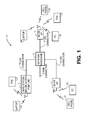
- FIG. 1 shows a communication system 10 that includes a plurality of base stations (BS) and/or access points (AP) 11 - 13 , a plurality of wireless communication devices 20 - 27 and a network hardware component 14 .
- the wireless communication devices 20 - 27 may be laptop computers 20 and 24 , personal digital assistants 21 and 27 , personal computers 23 and 26 , cellular telephones 22 and 25 , and/or any other type of device that supports wireless communications.
- the base stations or access points 11 - 13 may be operably coupled to network hardware 14 via respective local area network (LAN) connections 15 - 17 .
- Network hardware 14 which may be a router, switch, bridge, modem, system controller, etc., may provide a wide area network (WAN) connection 18 for communication system 10 .
- Individual base station or access point 11 - 13 generally has an associated antenna or antenna array to communicate with the wireless communication devices in its area.
- the wireless communication devices register with a particular base station or access point 11 - 13 to receive services within communication system 10 .
- wireless communication devices may communicate directly via an allocated channel.
- each wireless communication device includes a built-in radio and/or is coupled to a radio.
- the radio includes a highly linear amplifiers and/or programmable multi-stage amplifiers to enhance performance, reduce costs, reduce size, and/or enhance broadband applications.
- the radio also includes, or is coupled to, an antenna or antennas having a particular antenna coverage pattern for propagating of outbound RF signals and/or reception of inbound RF signals.
- FIG. 2 is a schematic block diagram illustrating part of a wireless communication device 100 that includes a transmitter (TX) 101 , receiver (RX) 102 and baseband module 105 .
- Baseband module 105 provides baseband processing operations.
- baseband module 105 is or includes a digital-signal-processor (DSP).
- DSP digital-signal-processor
- Baseband module 105 is typically coupled to a host unit, applications processor or other unit(s) that provides operational processing for the device and/or interface with a user.
- a host unit 110 is shown.
- device 100 may represent the computing portion of the computer, while device 110 is utilized to provide WiFi and/or Bluetooth components for communicating wirelessly between the computer and an access point and/or between the computer and a Bluetooth device.
- device 100 may represent the application portion of the handheld device, while device 100 is utilized to provide WiFi and/or Bluetooth components for communicating wirelessly between the handheld device and an access point and/or between the handheld device and a Bluetooth device.
- device 100 may represent the WiFi and/or Bluetooth components for the smartphone.
- Device 100 may also be used for cellular communication as well in some embodiments.
- device 100 may be incorporated in one or more of the wireless communication devices 20 - 27 shown in FIG. 1 .
- a memory 106 is shown coupled to baseband module 105 , which memory 106 may be utilized to store data, as well as program instructions that operate on baseband module 105 .
- Various types of memory devices may be utilized for memory 106 . It is to be noted that memory 106 may located anywhere within device 100 and, in one instance, it may also be part of baseband module 105 .
- Transmitter 101 and receiver 102 are coupled to an antenna array 104 via transmit/receive (T/R) switch module 103 .
- T/R switch module 103 switches the antenna array between the transmitter and receiver depending on the mode of operation. It is to be noted that in other embodiments, separate antenna arrays may be used for transmitter 101 and receiver 102 , respectively.
- Outbound data for transmission from host unit 110 are coupled to baseband module 105 and converted to baseband signals and then coupled to transmitter 101 .
- Transmitter 101 converts the baseband signals to outbound radio frequency (RF) signals for transmission from device 100 via antenna array 104 .
- Transmitter 101 may utilize one of a variety of up-conversion or modulation techniques to convert the outbound baseband signals to outbound RF signal.
- the conversion process is dependent on the particular communication standard or protocol being utilized.
- inbound RF signals are received by antenna array 104 and coupled to receiver 102 .
- Receiver 102 then converts the inbound RF signals to inbound baseband signals, which are then coupled to baseband module 105 .
- Receiver 102 may utilize one of a variety of down-conversion or demodulation techniques to convert the inbound RF signals to inbound baseband signals.
- the inbound baseband signals are processed by baseband module 105 and inbound data is output from baseband module 105 to host unit 110 .
- baseband module 105 , transmitter 101 and receiver 102 are integrated on the same integrated circuit (IC) chip.
- Transmitter 101 and receiver 102 are typically referred to as the RF front-end.
- one or more of these components may be on separate IC chips.
- other components shown in FIG. 2 may be incorporated on the same IC chip, along with baseband module 105 , transmitter 101 and receiver 102 .
- the antenna array 104 may also be incorporated on the same IC chip as well. As described below, in one embodiment, antenna array 104 is incorporated on a substrate separate from the device 100 , but the two are packaged together as one flip-chip assembly.
- SOC system-on-chip
- host devices, application processors and/or user interfaces, such as host unit 110 may be integrated on the same IC chip along with baseband module 105 , transmitter 101 and receiver 102 .
- antenna array 104 comprises a plurality of antenna elements disposed on a planar surface to form a planar antenna array structure.
- Substrate 201 is comprised of a dielectric or semi-conductive material that allows antenna elements 202 to be formed thereon.
- substrate 201 may be silicon, upon which conductive antenna elements are formed thereon.
- the substrate may be formed from an oxide material or even a printed circuit (PC) board.
- PC printed circuit
- attachment contacts 203 are utilized to provide a contact surface for attaching planar antenna array 200 to a supporting surface 212 .
- a variety of designs may be employed for attachment contacts 203 to attach planar antenna array 200 to supporting surface 212 .
- FIG. 4 illustrates an integrated circuit (IC) 210 attached to the underside of substrate 201 opposite the side containing planar antenna array 200 .
- IC 201 typically includes circuitry that provides the RF front end operations.
- IC 201 may include baseband processing as well.
- IC 210 may be device 100 of FIG. 2 that provides both RF and baseband processing operations.
- IC 210 is attached to substrate 201 and electrical connections made to substrate 201 through contacts 211 .
- contacts 211 In one embodiment, ball-grid-array (BGA) designs may be used for contacts 211 .
- flip-chip technology may be used for mounting IC 210 on the underside of the planar antenna array 200 .
- IC 210 may not be mated to substrate 201 .
- the example embodiment shown in FIG. 4 places device 100 proximal to planar antenna array 200 , such that the electrical connection between IC 210 and planar antenna array 200 is through substrate 201 . If IC 210 was placed away from substrate 201 , a significantly longer path would be present for signal transmission between IC 210 and planar antenna array 200 .
- FIG. 5 exemplifies a situation when planar antenna array 200 is in operation. Due to the nature of the planar surface, the antenna coverage pattern of planar antenna array 200 is generally in a vertical direction. The vertical direction is identified by axis Y, which is the axis normal (perpendicular) to the planar surface, upon which the antenna elements reside. Alternatively, axis X represents the horizontal direction, which is parallel to the planar surface. For a planar antenna array design, such as planar antenna array 200 , the coverage or pattern provided by the array is no more than approximately 60 degrees)(60° from vertical (or zenith).
- the coverage may be much less.
- the 60° or less coverage from the vertical is illustrated by angle a in FIG. 5 .
- the dark rotating arrow indicates that the coverage pattern is obtained 360° about the vertical.
- the extent of the antenna coverage does not extend further than the boundary shown by line 220 . This is generally the case, even if beamforming techniques are utilized to vary the coverage pattern of the antenna array 200 , since beamforming scans still operate in the perpendicular direction relative to the planar surface.
- FIG. 6 shows an antenna coverage pattern that is more varied than the coverage provided in FIG. 5 .
- the antenna coverage is in the approximate range of ⁇ 30° to +70° from the horizontal axis.
- the ⁇ 30° angle is illustrated by angle y and the +70° angle is illustrated by angle ⁇ .
- planar antenna array 200 would provide a coverage area bounded by boundary lines 230 and 231 .
- the dark rotating arrow indicates that the coverage pattern is obtained 360° about the vertical. It is evident from the illustrations of FIGS.
- FIG. 7 illustrates one embodiment for obtaining more horizontal coverage from planar antenna array 200 , such as the coverage pattern shown in FIG. 6 .
- a reflector 300 is disposed proximal and above planar antenna array 200 .
- Reflector 300 is made from a conductive material or, alternatively, has a conductive coating, so that signals emanating from the planar antenna array 200 are reflected back towards the planar antenna array 200 .
- Two example reflections are shown by lines 301 , 302 . It is understood that signals for reception by planar antenna array 200 may be reflected onto the planar antenna array along lines 301 , 302 , but in the reverse direction.
- antenna pattern coverage may be extended toward the horizontal direction and even below the plane of the horizontal.
- Reflector 300 is shown having a gull-wing shape, but other shapes may be utilized as well. For example, concave or convex shaped designs may be utilized in other embodiments. The shape and characteristics of reflector 300 is a matter of design choice, based on the extent of the antenna coverage desired for a particular signal transmission or reception.
- FIG. 8 illustrates another embodiment for obtaining a more horizontal coverage pattern from planar antenna array 200 .
- a lens element 400 is disposed proximal and above planar antenna array 200 .
- Lens element 400 is made from material that refracts signals when the signals cross the lens boundary. Two example refractions are shown by lines 401 and 402 . It is also understood that signals for reception by planar antenna array 200 may be refracted onto the planar antenna array 200 along lines 401 , 402 , but in the reverse direction.
- antenna coverage pattern may be extended toward the horizontal direction as well.
- Lens element 400 is shown having a substantially flat surface along an edge proximal to the planar antenna array 200 and a more rounded curvature at a distal edge away from planar antenna array 200 .
- the actual shape of the lens element 400 is a design choice, based on the refractive qualities desired for the signals to and from planar antenna array 200 .
- lens element 400 may be constructed from a variety of materials which provide refractive properties for the signal being transmitted or received by planar antenna array 200 .
- lens element 400 may be constructed from low-loss dielectric materials, glass, plastic, TeflonTM materials, as well as others.
- the height of the lens element 400 will depend on the particular coverage desired.
- both of these devices operably extend the antenna pattern coverage in the horizontal direction beyond the angle a noted in FIG. 5 .
- the antenna pattern coverage may be extended even below the planar surface of the antenna array, as shown in FIG. 7 .
- the coverage obtained approximates the ⁇ 30° to +70° coverage shown in FIG. 6 .
- a reflector or refractor element or device allows for a more extended coverage in the horizontal direction when compared to a planar antenna array without such reflector or refractor. It is to be noted that some embodiment for practicing the invention may employ combined reflective and refractive properties in a device disposed proximally above the planar antenna array.
- the reflective/refractive device may be a separate component that is placed within a housing or enclosure that also houses the planar antenna array.
- the planar antenna array may be mounted within a housing of a wireless apparatus and the reflective/refractive device is then attached to a portion of the enclosure that fits over the housing.
- FIG. 9 illustrates a notebook computer 500 that includes a housing 501 to hold the keyboard, battery, circuit boards etc. and a housing 502 that contains the display.
- planar antenna array 200 is placed within the housing 501 , which also houses the display.
- Either the reflector 300 or lens element 400 is positioned over the planar antenna array 200 .
- the drawing of FIG. 9 exemplifies lens element 400 , but the reflector 300 may be used as well.
- Reflector 300 or lens element 400 may be constructed as part of planar antenna array 200 or it may be part of, or attached to, housing 502 , so that when planar antenna array 200 is placed within housing 502 , reflector 300 or lens element 400 resides atop planar antenna array 200 .
- planar antenna array 200 is placed within housing 501 .
- FIG. 10 An example of such placement is shown in FIG. 10 .
- reflector 300 or lens element 400 may be constructed as part of planar antenna array 200 or it may be part of, or attached to, housing 501 , so that when planar antenna array 200 is placed within housing 501 , reflector 300 or lens element 400 resides atop planar antenna array 200 .
- One advantage of utilizing the arrangement shown in FIG. 10 is that assembly containing planar antenna array 200 and IC 201 is much closer to the computer circuitry housed within housing 501 , so that electrical connections between IC 201 and the computer circuitry may be minimized.
- FIG. 11 shows a pictorial illustration of the one example embodiment of FIG. 10 , in which planar antenna array 200 is mounted within housing 501 of notebook computer 500 .
- planar antenna array 200 is mounted flat within housing 501 , the presence of reflector 300 or lens element 400 allows antenna coverage along the horizontal direction.
- an aperture 510 may be placed along the side of the housing 501 to allow passage of wireless signals. Since horizontal coverage is available from planar antenna array 200 , signal coverage is maintained by planar antenna array 200 in this instance through aperture 510 .
- planar antenna array 200 may be utilized with other wireless devices as well.
- FIG. 12 shows a handheld wireless device 600 , such as a media player, smartphone, etc. that incorporates planar antenna array 200 within its housing 610 .
- An aperture may be used as well, if needed due to the construction material of the housing.
- planar antenna array 200 may incorporate the planar antenna array 200 with the accompanying reflector 300 or lens element 400 .
- the presence of reflector 300 or lens element 400 above planar antenna array 200 allows for a more wider coverage by the planar antenna array 200 .
- wider coverage allows the planar antenna array 200 to be placed at certain locations, which would not be possible if the wider coverage was not present.
- Such configuration may reduce cost and/or reduce implementation complexity, thereby enhancing the performance of the platform containing the planar antenna array.
- the terms “substantially” and “approximately” provides an industry-accepted tolerance for its corresponding term and/or relativity between items. Such an industry-accepted tolerance ranges from less than one percent to fifty percent. Such relativity between items ranges from a difference of a few percent to magnitude differences.
- the term(s) “coupled” and/or “coupling” includes direct coupling between items and/or indirect coupling between items via an intervening item (e.g., an item includes, but is not limited to, a component, an element, a circuit, and/or a module) where, for indirect coupling, the intervening item does not modify the information of a signal but may adjust its current level, voltage level, and/or power level.
- an intervening item e.g., an item includes, but is not limited to, a component, an element, a circuit, and/or a module
- inferred coupling i.e., where one element is coupled to another element by inference
- inferred coupling includes direct and indirect coupling between two items in the same manner as “coupled to”.
- the term “operable to” indicates that an item includes one or more of power connections, input(s), output(s), etc., to perform one or more its corresponding functions and may further include inferred coupling to one or more other items.
Landscapes
- Engineering & Computer Science (AREA)
- Computer Hardware Design (AREA)
- Computer Networks & Wireless Communication (AREA)
- Physics & Mathematics (AREA)
- Electromagnetism (AREA)
- General Engineering & Computer Science (AREA)
- Variable-Direction Aerials And Aerial Arrays (AREA)
Abstract
Description
- 1. Technical Field of the Invention
- The embodiments of the invention relate to planar antenna arrays and, more particularly, to the utilization of a planar antenna array to provide platform enhancements.
- 2. Description of Related Art
- Various wireless communication systems are known today to provide links between devices, whether directly or through a network. Such communication systems range from national and/or international cellular telephone systems, the Internet, point-to-point in-home system, as well as other systems. Communication systems typically operate in accordance with one or more communication standards or protocol. For instance, wireless communication systems may operate using protocols, such as IEEE 802.11, Bluetooth™, advanced mobile phone services (AMPS), digital AMPS, global system for mobile communications (GSM), code division multiple access (CDMA), local multi-point distribution systems (LMDS), multi-channel-multi-point distribution systems (MMDS), as well as others.
- For each wireless communication device to participate in wireless communications, it generally includes a built-in radio transceiver (i.e., receiver and transmitter) or is coupled to an associated radio transceiver (e.g., a station for in-home and/or in-building wireless communication networks, modem, etc.). Typically, the transceiver includes a baseband processing stage and a radio frequency (RF) stage. The baseband processing provides the conversion from data to baseband signals for transmitting and baseband signals to data for receiving, in accordance with a particular wireless communication protocol. The baseband processing stage is coupled to a RF stage (transmitter section and receiver section) that provides the conversion between the baseband signals and RF signals. The RF stage may be a direct conversion transceiver that converts directly between baseband and RF or may include one or more intermediate frequency stage(s).
- Furthermore, wireless devices typically operate within certain radio frequency ranges or band established by one or more communications standards or protocols. A local oscillator generally provides a local oscillation signal that is used to mix with received RF signals or baseband signals that are to be converted to RF signals in the modulation/demodulation stage of the RF front end. A synthesizer may be used to set the frequencies to drive the local oscillator to provide the desired frequencies for mixing, in which the desired frequencies are generally based on the channel frequencies established for the particular standard or protocol.
- In a typical wireless device, the RF transceiver is coupled to an antenna. In some earlier portable devices, such as cordless telephones and radios, the antenna was an elongated di-pole antenna or a loop antenna. The antenna was usually located external to the device. In more recent wireless devices, such as cellular phones, portable computers, handheld audio and/or video players, the antenna is mounted internally. For example, in notebook computers, the WiFi antenna is mounted around the display or along an edge of the computer housing. In cellular phones, the antenna is disposed along the side edge or along the top of the phone casing. Most of these antennas utilize an elongated coil or a helical coil.
- Devices today that communicate short range, such as those devices that utilize 802.11 protocol or Bluetooth™ protocol, generally utilize antennas that provide omni-directional coverage so that a particular position of the devices is typically not a concern. Thus, a notebook computer utilizing one of the 802.11 protocols may be placed in a general proximity to an access point, such as a router, without regard to positioning or facing of the computer in a particular way. A headset utilizing Bluetooth protocol may be worn on a person and the associated communicating device may be placed nearby or on the person, without regard to the placement of the device or particular facing by the user. The omni-directional antenna coverage is easily obtainable using wire or coil antennas, because these devices typically use communication protocols that are within the 2-6 GHz band.
- As demand for data downloads increase, newer generation devices are being developed that allow for higher data transfers. These higher data rate mobile devices will most likely use communication protocols that require a higher frequency of operation. In that instance, standard coil antennas may not provide the requisite communication linkage capability. For example, devices that utilize millimeter wave protocols in the 60+ GHz range may need to transition to an array of antennas to provide the transmission and reception capabilities. Antenna arrays allow for improved beamforming characteristics at such higher frequencies, but have the drawback in that theses arrays are typically formed on a planar substrate and may be more directional than coil type antennas. In this instance, relative positioning of the mobile device could be a concern in order to maintain a communication link with other communicating devices, if the antenna pattern generated by the planar array is restrictive.
- Accordingly, there is a need to obtain larger antenna coverage pattern from an antenna, where such an antenna utilizes a planar antenna array.
- The present invention is directed to apparatus and methods of operation that are further described in the following Brief Description of the Drawings, the Detailed Description of the Invention, and the Claims. Other features and advantages of the present invention will become apparent from the following detailed description of the embodiments of the invention made with reference to the accompanying drawings.
-
FIG. 1 is a block diagram showing a wireless communication system in accordance with one embodiment for practicing the present invention. -
FIG. 2 is a schematic block diagram showing an embodiment of a wireless communication device for practicing the present invention, in which a planar antenna array is utilized. -
FIG. 3 is a pictorial illustration of one embodiment of a planar antenna array assembly comprised of a plurality of antennas formed on a planar surface. -
FIG. 4 is a side plan view of the antenna array assembly of Figure of 3, which is mounted on a supporting surface. -
FIG. 5 is a pictorial illustration showing typical beam coverage from a planar antenna array structure. -
FIG. 6 is a pictorial illustration showing a more desired beam coverage from a planar antenna array structure. -
FIG. 7 illustrates one embodiment for practicing the invention, in which a reflector is positioned above a planar antenna array to redirect beam direction to obtain a more horizontal antenna coverage pattern from the planar antenna array. -
FIG. 8 illustrates one embodiment for practicing the invention, in which a refractive lens element is positioned above a planar antenna array to redirect beam direction to obtain a more horizontal antenna coverage pattern from the planar antenna array. -
FIG. 9 illustrates a disposition of the planar antenna array assembly utilizing the lens element ofFIG. 8 within a display casing portion of a notebook computer, according to one embodiment of the invention. -
FIG. 10 illustrates a disposition of the antenna array assembly utilizing the lens element ofFIG. 8 within a keyboard casing portion of a notebook computer, according to one embodiment of the invention. -
FIG. 11 is a pictorial diagram illustrating a disposition of the planar antenna array assembly within the keyboard casing portion of the notebook computer, according to one embodiment of the invention. -
FIG. 12 is a pictorial diagram illustrating a disposition of the planar antenna array assembly within a mobile handheld device according to one embodiment of the invention, according to one embodiment of the invention. - The embodiments of the present invention may be practiced in a variety of wireless devices that utilize antennas arranged on a planar surface. The particular embodiments described below pertain to antenna elements disposed into an array and formed on a planar surface. However, the invention may be practiced with various types of antennas that have a flat disposition and a limited antenna pattern. Furthermore, two beam changing examples are described below in way of a reflector and a lens. However, it is to be noted that other elements or devices which change the direction of the beam to and/or from a planar antenna assembly may be employed as well in practicing the invention.
-
FIG. 1 illustrates one environment for practicing the present invention.FIG. 1 shows acommunication system 10 that includes a plurality of base stations (BS) and/or access points (AP) 11-13, a plurality of wireless communication devices 20-27 and anetwork hardware component 14. The wireless communication devices 20-27 may belaptop computers digital assistants personal computers cellular telephones 22 and 25, and/or any other type of device that supports wireless communications. - The base stations or access points 11-13 may be operably coupled to
network hardware 14 via respective local area network (LAN) connections 15-17.Network hardware 14, which may be a router, switch, bridge, modem, system controller, etc., may provide a wide area network (WAN)connection 18 forcommunication system 10. Individual base station or access point 11-13 generally has an associated antenna or antenna array to communicate with the wireless communication devices in its area. Typically, the wireless communication devices register with a particular base station or access point 11-13 to receive services withincommunication system 10. For direct connections (i.e., point-to-point communications), wireless communication devices may communicate directly via an allocated channel. - Typically, base stations are used for cellular telephone systems and like-type systems, while access points are used for in-home or in-building wireless networks. Regardless of the particular type of communication system, each wireless communication device includes a built-in radio and/or is coupled to a radio. The radio includes a highly linear amplifiers and/or programmable multi-stage amplifiers to enhance performance, reduce costs, reduce size, and/or enhance broadband applications. The radio also includes, or is coupled to, an antenna or antennas having a particular antenna coverage pattern for propagating of outbound RF signals and/or reception of inbound RF signals.
-
FIG. 2 is a schematic block diagram illustrating part of awireless communication device 100 that includes a transmitter (TX) 101, receiver (RX) 102 andbaseband module 105.Baseband module 105 provides baseband processing operations. In some embodiments,baseband module 105 is or includes a digital-signal-processor (DSP).Baseband module 105 is typically coupled to a host unit, applications processor or other unit(s) that provides operational processing for the device and/or interface with a user. InFIG. 1 , ahost unit 110 is shown. For example, in a notebook or laptop computer,device 100 may represent the computing portion of the computer, whiledevice 110 is utilized to provide WiFi and/or Bluetooth components for communicating wirelessly between the computer and an access point and/or between the computer and a Bluetooth device. Similarly, for a handheld audio or video device,device 100 may represent the application portion of the handheld device, whiledevice 100 is utilized to provide WiFi and/or Bluetooth components for communicating wirelessly between the handheld device and an access point and/or between the handheld device and a Bluetooth device. Alternatively, for a mobile telephone, such as a smartphone,device 100 may represent the WiFi and/or Bluetooth components for the smartphone.Device 100 may also be used for cellular communication as well in some embodiments. Furthermore,device 100 may be incorporated in one or more of the wireless communication devices 20-27 shown inFIG. 1 . - A
memory 106 is shown coupled tobaseband module 105, whichmemory 106 may be utilized to store data, as well as program instructions that operate onbaseband module 105. Various types of memory devices may be utilized formemory 106. It is to be noted thatmemory 106 may located anywhere withindevice 100 and, in one instance, it may also be part ofbaseband module 105. -
Transmitter 101 andreceiver 102 are coupled to anantenna array 104 via transmit/receive (T/R)switch module 103. T/R switch module 103 switches the antenna array between the transmitter and receiver depending on the mode of operation. It is to be noted that in other embodiments, separate antenna arrays may be used fortransmitter 101 andreceiver 102, respectively. - Outbound data for transmission from
host unit 110 are coupled tobaseband module 105 and converted to baseband signals and then coupled totransmitter 101.Transmitter 101 converts the baseband signals to outbound radio frequency (RF) signals for transmission fromdevice 100 viaantenna array 104.Transmitter 101 may utilize one of a variety of up-conversion or modulation techniques to convert the outbound baseband signals to outbound RF signal. - Generally, the conversion process is dependent on the particular communication standard or protocol being utilized.
- In a similar manner, inbound RF signals are received by
antenna array 104 and coupled toreceiver 102.Receiver 102 then converts the inbound RF signals to inbound baseband signals, which are then coupled tobaseband module 105.Receiver 102 may utilize one of a variety of down-conversion or demodulation techniques to convert the inbound RF signals to inbound baseband signals. The inbound baseband signals are processed bybaseband module 105 and inbound data is output frombaseband module 105 tohost unit 110. - It is to be noted that in one embodiment,
baseband module 105,transmitter 101 andreceiver 102 are integrated on the same integrated circuit (IC) chip.Transmitter 101 andreceiver 102 are typically referred to as the RF front-end. In other embodiments, one or more of these components may be on separate IC chips. Similarly, other components shown inFIG. 2 may be incorporated on the same IC chip, along withbaseband module 105,transmitter 101 andreceiver 102. In some embodiments, theantenna array 104 may also be incorporated on the same IC chip as well. As described below, in one embodiment,antenna array 104 is incorporated on a substrate separate from thedevice 100, but the two are packaged together as one flip-chip assembly. Furthermore, with advent of system-on-chip (SOC) integration, host devices, application processors and/or user interfaces, such ashost unit 110, may be integrated on the same IC chip along withbaseband module 105,transmitter 101 andreceiver 102. - Additionally, although one
transmitter 101 andreceiver 102 are shown, it is to be noted that other embodiments may utilize multiple transmitter units and receiver units. For example, diversity communication and/or multiple input and/or multiple output communications, such as multiple-input-multiple-output (MIMO) communication, may utilizemultiple transmitters 101 and/orreceivers 102 as part of the RF front-end. As will be described below, in one embodiment,antenna array 104 comprises a plurality of antenna elements disposed on a planar surface to form a planar antenna array structure. -
FIG. 3 shows aplanar antenna array 200 comprised of a plurality ofantenna elements 202 disposed on a planar surface of asubstrate 201. Eachantenna element 202 may be fabricated utilizing a variety of techniques, including known techniques. Generally, a conductive pattern or design is disposed within or atopsubstrate 201 to fabricate eachantenna element 202. Theantenna elements 202 are then electrically coupled to a transmitter and/or receiver, such as described forantenna element 104 inFIG. 2 . In the shown example ofFIG. 3 , sixteenantenna elements 202 are shown arranged in a 4×4 matrix. It is to be noted that other embodiments may use different number of elements and the elements may be arranged differently. In one embodiment, the sixteenantenna elements 202 are disposed on a 12 millimeter by 12 millimeter surface. -
Substrate 201 is comprised of a dielectric or semi-conductive material that allowsantenna elements 202 to be formed thereon. For example, in one embodiment,substrate 201 may be silicon, upon which conductive antenna elements are formed thereon. In other embodiments, the substrate may be formed from an oxide material or even a printed circuit (PC) board. The actual material that formssubstrate 201 andantenna elements 202 are not critical to the practice of the present invention, suffice that a plurality ofantenna elements 202 are formed on a support body, such assubstrate 201, to provide a substantiallyplanar antenna array 200 and electrical connections are provided withinsubstrate 201 for electrical coupling ofantenna array 200. - As noted in
FIG. 3 , in one embodiment, a plurality of attachment points orcontacts 203 are shown on the underside ofsubstrate 201. As shown inFIG. 4 ,attachment contacts 203 are utilized to provide a contact surface for attachingplanar antenna array 200 to a supportingsurface 212. A variety of designs may be employed forattachment contacts 203 to attachplanar antenna array 200 to supportingsurface 212. -
FIG. 4 illustrates an integrated circuit (IC) 210 attached to the underside ofsubstrate 201 opposite the side containingplanar antenna array 200.IC 201 typically includes circuitry that provides the RF front end operations. In some embodiments,IC 201 may include baseband processing as well. Accordingly, in one embodiment,IC 210 may bedevice 100 ofFIG. 2 that provides both RF and baseband processing operations.IC 210 is attached tosubstrate 201 and electrical connections made tosubstrate 201 throughcontacts 211. In one embodiment, ball-grid-array (BGA) designs may be used forcontacts 211. In one embodiment, flip-chip technology may be used for mountingIC 210 on the underside of theplanar antenna array 200. - It is to be noted that in some
instances IC 210 may not be mated tosubstrate 201. However, for better performance characteristics, it is generally advantageous to have short transmission distance between an antenna and the RF front-end to reduce loss, noise, distortion etc., which may degrade performance. Accordingly, the example embodiment shown inFIG. 4 , placesdevice 100 proximal toplanar antenna array 200, such that the electrical connection betweenIC 210 andplanar antenna array 200 is throughsubstrate 201. IfIC 210 was placed away fromsubstrate 201, a significantly longer path would be present for signal transmission betweenIC 210 andplanar antenna array 200. -
FIG. 5 exemplifies a situation whenplanar antenna array 200 is in operation. Due to the nature of the planar surface, the antenna coverage pattern ofplanar antenna array 200 is generally in a vertical direction. The vertical direction is identified by axis Y, which is the axis normal (perpendicular) to the planar surface, upon which the antenna elements reside. Alternatively, axis X represents the horizontal direction, which is parallel to the planar surface. For a planar antenna array design, such asplanar antenna array 200, the coverage or pattern provided by the array is no more than approximately 60 degrees)(60° from vertical (or zenith). - With some planar antenna arrays, the coverage may be much less. The 60° or less coverage from the vertical is illustrated by angle a in
FIG. 5 . The dark rotating arrow indicates that the coverage pattern is obtained 360° about the vertical. Thus, the extent of the antenna coverage does not extend further than the boundary shown byline 220. This is generally the case, even if beamforming techniques are utilized to vary the coverage pattern of theantenna array 200, since beamforming scans still operate in the perpendicular direction relative to the planar surface. -
FIG. 6 shows an antenna coverage pattern that is more varied than the coverage provided inFIG. 5 . In the example ofFIG. 6 , the antenna coverage is in the approximate range of −30° to +70° from the horizontal axis. The −30° angle is illustrated by angle y and the +70° angle is illustrated by angle β. Thus, with this coverage pattern,planar antenna array 200 would provide a coverage area bounded byboundary lines FIGS. 4 and 5 , that the coverage area bounded bylines 230, 231 (approximately −30° to +70° from the horizontal axis) is not only larger in area, but provides coverage in both the horizontal and vertical directions, whereas the coverage area between axis Y andline 220 is more in the vertical direction. Accordingly, although it may not be fully omni-directional, the antenna coverage area shown inFIG. 6 is closer to providing more of an omni-directional coverage than the pattern shown inFIG. 5 .FIGS. 7 and 8 illustrate two example embodiments for obtaining a more extended antenna coverage from a planar antenna array, such asplanar antenna array 200. -
FIG. 7 illustrates one embodiment for obtaining more horizontal coverage fromplanar antenna array 200, such as the coverage pattern shown inFIG. 6 . In the particular example, areflector 300 is disposed proximal and aboveplanar antenna array 200.Reflector 300 is made from a conductive material or, alternatively, has a conductive coating, so that signals emanating from theplanar antenna array 200 are reflected back towards theplanar antenna array 200. Two example reflections are shown bylines planar antenna array 200 may be reflected onto the planar antenna array alonglines reflector 300, antenna pattern coverage may be extended toward the horizontal direction and even below the plane of the horizontal. -
Reflector 300 is shown having a gull-wing shape, but other shapes may be utilized as well. For example, concave or convex shaped designs may be utilized in other embodiments. The shape and characteristics ofreflector 300 is a matter of design choice, based on the extent of the antenna coverage desired for a particular signal transmission or reception. -
FIG. 8 illustrates another embodiment for obtaining a more horizontal coverage pattern fromplanar antenna array 200. In the particular example, alens element 400 is disposed proximal and aboveplanar antenna array 200.Lens element 400 is made from material that refracts signals when the signals cross the lens boundary. Two example refractions are shown bylines planar antenna array 200 may be refracted onto theplanar antenna array 200 alonglines lens element 400, antenna coverage pattern may be extended toward the horizontal direction as well. -
Lens element 400 is shown having a substantially flat surface along an edge proximal to theplanar antenna array 200 and a more rounded curvature at a distal edge away fromplanar antenna array 200. However, the actual shape of thelens element 400 is a design choice, based on the refractive qualities desired for the signals to and fromplanar antenna array 200. Likewise,lens element 400 may be constructed from a variety of materials which provide refractive properties for the signal being transmitted or received byplanar antenna array 200. For example,lens element 400 may be constructed from low-loss dielectric materials, glass, plastic, Teflon™ materials, as well as others. Similarly, the height of thelens element 400 will depend on the particular coverage desired. In one embodiment, lens element has a thickness of atlease 10 millimeters and covers substantially the surface area ofantenna elements 202. In another embodiment,lens element 400 is approximately twice the size of theplanar antenna array 200 to ensure full coverage over theantenna elements 202. Again, the actual size, shape and composition oflens element 400 is a design choice based on the particular planar antenna array used and the signals being transmitted and/or received. Furthermore, although a lens element is described herein, a variety of other types of devices that refract RF signals may be utilized in place oflens element 400 in other embodiments. - Whether a reflector or a refractor element is utilized over the planar antenna array, both of these devices operably extend the antenna pattern coverage in the horizontal direction beyond the angle a noted in
FIG. 5 . With sufficient consideration, the antenna pattern coverage may be extended even below the planar surface of the antenna array, as shown inFIG. 7 . In one embodiment, the coverage obtained approximates the −30° to +70° coverage shown inFIG. 6 . - Accordingly, the utilization of a reflector or refractor element or device allows for a more extended coverage in the horizontal direction when compared to a planar antenna array without such reflector or refractor. It is to be noted that some embodiment for practicing the invention may employ combined reflective and refractive properties in a device disposed proximally above the planar antenna array.
- The reflective/refractive device that is disposed above the planar antenna array may be structurally made as part of the planar antenna array assembly or, alternatively, made as a separate component. If made part of the planar antenna array assembly, the reflective/refractive device may be mounted above the planar antenna array by some support member according to one embodiment. In another embodiment, an adhesive may be used to affix the reflector/refractor on to the planar antenna array. Still in other embodiments, the reflective/refractive device may be placed in an enclosed package.
- Alternatively, the reflective/refractive device may be a separate component that is placed within a housing or enclosure that also houses the planar antenna array. For example, the planar antenna array may be mounted within a housing of a wireless apparatus and the reflective/refractive device is then attached to a portion of the enclosure that fits over the housing. Many other examples abound.
- As a further example,
FIG. 9 illustrates anotebook computer 500 that includes ahousing 501 to hold the keyboard, battery, circuit boards etc. and ahousing 502 that contains the display. In this example,planar antenna array 200 is placed within thehousing 501, which also houses the display. Either thereflector 300 orlens element 400 is positioned over theplanar antenna array 200. Note that the drawing ofFIG. 9 exemplifieslens element 400, but thereflector 300 may be used as well.Reflector 300 orlens element 400 may be constructed as part ofplanar antenna array 200 or it may be part of, or attached to,housing 502, so that whenplanar antenna array 200 is placed withinhousing 502,reflector 300 orlens element 400 resides atopplanar antenna array 200. - In another example,
planar antenna array 200, withreflector 300 orlens element 400, is placed withinhousing 501. An example of such placement is shown inFIG. 10 . Again,reflector 300 orlens element 400 may be constructed as part ofplanar antenna array 200 or it may be part of, or attached to,housing 501, so that whenplanar antenna array 200 is placed withinhousing 501,reflector 300 orlens element 400 resides atopplanar antenna array 200. One advantage of utilizing the arrangement shown inFIG. 10 is that assembly containingplanar antenna array 200 andIC 201 is much closer to the computer circuitry housed withinhousing 501, so that electrical connections betweenIC 201 and the computer circuitry may be minimized.FIG. 11 shows a pictorial illustration of the one example embodiment ofFIG. 10 , in whichplanar antenna array 200 is mounted withinhousing 501 ofnotebook computer 500. - Although the
planar antenna array 200 is mounted flat withinhousing 501, the presence ofreflector 300 orlens element 400 allows antenna coverage along the horizontal direction. In some instances where the housing is made from a metallic material that inhibits passage of wireless signals, anaperture 510 may be placed along the side of thehousing 501 to allow passage of wireless signals. Since horizontal coverage is available fromplanar antenna array 200, signal coverage is maintained byplanar antenna array 200 in this instance throughaperture 510. - Likewise,
planar antenna array 200 may be utilized with other wireless devices as well.FIG. 12 shows ahandheld wireless device 600, such as a media player, smartphone, etc. that incorporatesplanar antenna array 200 within itshousing 610. An aperture may be used as well, if needed due to the construction material of the housing. - Accordingly, a variety of devices may incorporate the
planar antenna array 200 with the accompanyingreflector 300 orlens element 400. The presence ofreflector 300 orlens element 400 aboveplanar antenna array 200 allows for a more wider coverage by theplanar antenna array 200. In some instances, such wider coverage allows theplanar antenna array 200 to be placed at certain locations, which would not be possible if the wider coverage was not present. Such configuration may reduce cost and/or reduce implementation complexity, thereby enhancing the performance of the platform containing the planar antenna array. - As may be used herein, the terms “substantially” and “approximately” provides an industry-accepted tolerance for its corresponding term and/or relativity between items. Such an industry-accepted tolerance ranges from less than one percent to fifty percent. Such relativity between items ranges from a difference of a few percent to magnitude differences. As may also be used herein, the term(s) “coupled” and/or “coupling” includes direct coupling between items and/or indirect coupling between items via an intervening item (e.g., an item includes, but is not limited to, a component, an element, a circuit, and/or a module) where, for indirect coupling, the intervening item does not modify the information of a signal but may adjust its current level, voltage level, and/or power level. As may further be used herein, inferred coupling (i.e., where one element is coupled to another element by inference) includes direct and indirect coupling between two items in the same manner as “coupled to”. As may even further be used herein, the term “operable to” indicates that an item includes one or more of power connections, input(s), output(s), etc., to perform one or more its corresponding functions and may further include inferred coupling to one or more other items.
- The embodiments of the present invention have been described above with the aid of functional building blocks illustrating the performance of certain functions. The boundaries of these functional building blocks have been arbitrarily defined for convenience of description.
- Alternate boundaries could be defined as long as the certain functions are appropriately performed. One of ordinary skill in the art may also recognize that the functional building blocks, and other illustrative blocks, modules and components herein, may be implemented as illustrated or by discrete components, application specific integrated circuits, processors executing appropriate software and the like or any combination thereof.
Claims (17)
Priority Applications (1)
| Application Number | Priority Date | Filing Date | Title |
|---|---|---|---|
| US13/077,210 US8638263B2 (en) | 2011-03-31 | 2011-03-31 | Platform enhancements for planar array antennas |
Applications Claiming Priority (1)
| Application Number | Priority Date | Filing Date | Title |
|---|---|---|---|
| US13/077,210 US8638263B2 (en) | 2011-03-31 | 2011-03-31 | Platform enhancements for planar array antennas |
Publications (2)
| Publication Number | Publication Date |
|---|---|
| US20120249388A1 true US20120249388A1 (en) | 2012-10-04 |
| US8638263B2 US8638263B2 (en) | 2014-01-28 |
Family
ID=46926492
Family Applications (1)
| Application Number | Title | Priority Date | Filing Date |
|---|---|---|---|
| US13/077,210 Active 2032-02-20 US8638263B2 (en) | 2011-03-31 | 2011-03-31 | Platform enhancements for planar array antennas |
Country Status (1)
| Country | Link |
|---|---|
| US (1) | US8638263B2 (en) |
Cited By (20)
| Publication number | Priority date | Publication date | Assignee | Title |
|---|---|---|---|---|
| US20160351996A1 (en) * | 2015-05-26 | 2016-12-01 | Qualcomm Incorporated | Antenna structures for wireless communications |
| US9666952B2 (en) | 2014-05-07 | 2017-05-30 | Panasonic Intellectual Property Management Co., Ltd. | Antenna device |
| WO2017119643A1 (en) | 2016-01-07 | 2017-07-13 | Samsung Electronics Co., Ltd. | Electronic device with antenna device |
| WO2018095535A1 (en) * | 2016-11-25 | 2018-05-31 | Sony Mobile Communications Inc. | Vertical antenna patch in cavity region |
| US20180212645A1 (en) * | 2015-09-25 | 2018-07-26 | Intel Corporation | Microelectronic package with wireless interconnect |
| US20180241132A1 (en) * | 2017-02-21 | 2018-08-23 | Taoglas Group Holdings Limited | Radar lens antenna arrays and methods |
| US10437295B1 (en) * | 2012-09-25 | 2019-10-08 | Micro Mobio Corporation | Personal cloud case cover with a plurality of modular capabilities |
| CN110495049A (en) * | 2016-12-30 | 2019-11-22 | 三星电子株式会社 | Beamforming auxiliary unit for antenna and terminal including same |
| KR20200077264A (en) * | 2018-12-20 | 2020-06-30 | 삼성전자주식회사 | Electronic device with antenna |
| EP3696912A1 (en) * | 2019-02-13 | 2020-08-19 | Samsung Electronics Co., Ltd. | Electronic device comprising antenna |
| CN111614388A (en) * | 2019-02-25 | 2020-09-01 | Oppo广东移动通信有限公司 | Electronic equipment and antenna performance adjustment method |
| CN111989822A (en) * | 2018-04-12 | 2020-11-24 | 松下知识产权经营株式会社 | Antenna device |
| US11058326B1 (en) | 2012-09-25 | 2021-07-13 | Micro Mobio Corporation | Cloud communication antenna panel system and method |
| US11322854B2 (en) * | 2018-02-02 | 2022-05-03 | Samsung Electronics Co., Ltd. | Antenna module comprising reflector, and electronic device comprising same |
| US20220345902A1 (en) * | 2021-04-23 | 2022-10-27 | Htc Corporation | Wireless signal transceiver |
| US11553857B1 (en) | 2012-09-25 | 2023-01-17 | Micro Mobio Corporation | System and method for through window personal cloud transmission |
| US11642045B1 (en) | 2012-09-25 | 2023-05-09 | Micro Mobio Corporation | Personal health and environmental monitoring device and method |
| WO2023048899A3 (en) * | 2021-09-07 | 2023-05-19 | Kokanee Research Llc | Electronic devices with millimeter wave antennas |
| US11786146B1 (en) | 2012-09-25 | 2023-10-17 | Micro Mobio Corporation | Wireless hub system and method |
| US12138041B1 (en) | 2012-09-25 | 2024-11-12 | Micro Mobio Corporation | Mobile device case with satellite communication capability |
Citations (6)
| Publication number | Priority date | Publication date | Assignee | Title |
|---|---|---|---|---|
| US20070200764A1 (en) * | 2006-02-24 | 2007-08-30 | Motonix Co., Ltd. | Multilayer planar array antenna |
| US20090046017A1 (en) * | 2007-08-15 | 2009-02-19 | Senglee Foo | Dual polarization antenna element with dielectric bandwidth compensation and improved cross-coupling |
| US20090096702A1 (en) * | 2007-10-16 | 2009-04-16 | Bill Vassilakis | Dual beam sector antenna array with low loss beam forming network |
| US7705797B2 (en) * | 2006-07-07 | 2010-04-27 | Iti Scotland Limited | Antenna arrangement |
| US7812767B2 (en) * | 2004-09-07 | 2010-10-12 | Nippon Telegraph And Telephone Corporation | Antenna device, array antenna device using the antenna device, module, module array and package module |
| US8208980B2 (en) * | 2008-11-06 | 2012-06-26 | Pong Research Corporation | Radiation redirecting external case for portable communication device and antenna embedded in battery of portable communication device |
-
2011
- 2011-03-31 US US13/077,210 patent/US8638263B2/en active Active
Patent Citations (6)
| Publication number | Priority date | Publication date | Assignee | Title |
|---|---|---|---|---|
| US7812767B2 (en) * | 2004-09-07 | 2010-10-12 | Nippon Telegraph And Telephone Corporation | Antenna device, array antenna device using the antenna device, module, module array and package module |
| US20070200764A1 (en) * | 2006-02-24 | 2007-08-30 | Motonix Co., Ltd. | Multilayer planar array antenna |
| US7705797B2 (en) * | 2006-07-07 | 2010-04-27 | Iti Scotland Limited | Antenna arrangement |
| US20090046017A1 (en) * | 2007-08-15 | 2009-02-19 | Senglee Foo | Dual polarization antenna element with dielectric bandwidth compensation and improved cross-coupling |
| US20090096702A1 (en) * | 2007-10-16 | 2009-04-16 | Bill Vassilakis | Dual beam sector antenna array with low loss beam forming network |
| US8208980B2 (en) * | 2008-11-06 | 2012-06-26 | Pong Research Corporation | Radiation redirecting external case for portable communication device and antenna embedded in battery of portable communication device |
Cited By (42)
| Publication number | Priority date | Publication date | Assignee | Title |
|---|---|---|---|---|
| US12138041B1 (en) | 2012-09-25 | 2024-11-12 | Micro Mobio Corporation | Mobile device case with satellite communication capability |
| US11786146B1 (en) | 2012-09-25 | 2023-10-17 | Micro Mobio Corporation | Wireless hub system and method |
| US11642045B1 (en) | 2012-09-25 | 2023-05-09 | Micro Mobio Corporation | Personal health and environmental monitoring device and method |
| US11553857B1 (en) | 2012-09-25 | 2023-01-17 | Micro Mobio Corporation | System and method for through window personal cloud transmission |
| US11058326B1 (en) | 2012-09-25 | 2021-07-13 | Micro Mobio Corporation | Cloud communication antenna panel system and method |
| US10437295B1 (en) * | 2012-09-25 | 2019-10-08 | Micro Mobio Corporation | Personal cloud case cover with a plurality of modular capabilities |
| US9666952B2 (en) | 2014-05-07 | 2017-05-30 | Panasonic Intellectual Property Management Co., Ltd. | Antenna device |
| US10361476B2 (en) * | 2015-05-26 | 2019-07-23 | Qualcomm Incorporated | Antenna structures for wireless communications |
| US20160351996A1 (en) * | 2015-05-26 | 2016-12-01 | Qualcomm Incorporated | Antenna structures for wireless communications |
| TWI712151B (en) * | 2015-09-25 | 2020-12-01 | 美商英特爾公司 | Microelectronic package with wireless interconnect |
| US20180212645A1 (en) * | 2015-09-25 | 2018-07-26 | Intel Corporation | Microelectronic package with wireless interconnect |
| TWI699106B (en) * | 2015-09-25 | 2020-07-11 | 美商英特爾公司 | Patch on interposer package with wireless communication interface |
| US10327268B2 (en) * | 2015-09-25 | 2019-06-18 | Intel Corporation | Microelectronic package with wireless interconnect |
| US11737154B2 (en) | 2015-09-25 | 2023-08-22 | Intel Corporation | Patch on interposer package with wireless communication interface |
| US10297900B2 (en) | 2016-01-07 | 2019-05-21 | Samsung Electronics Co., Ltd. | Electronic device with antenna device |
| WO2017119643A1 (en) | 2016-01-07 | 2017-07-13 | Samsung Electronics Co., Ltd. | Electronic device with antenna device |
| US11223104B2 (en) | 2016-01-07 | 2022-01-11 | Samsung Electronics Co., Ltd. | Electronic device with antenna device |
| CN108432041A (en) * | 2016-01-07 | 2018-08-21 | 三星电子株式会社 | Electronic equipment with antenna assembly |
| EP3369130A4 (en) * | 2016-01-07 | 2018-11-21 | Samsung Electronics Co., Ltd. | Electronic device with antenna device |
| WO2018095535A1 (en) * | 2016-11-25 | 2018-05-31 | Sony Mobile Communications Inc. | Vertical antenna patch in cavity region |
| US10879592B2 (en) | 2016-11-25 | 2020-12-29 | Sony Mobile Communications Inc. | Vertical antenna patch in cavity region |
| CN110495049A (en) * | 2016-12-30 | 2019-11-22 | 三星电子株式会社 | Beamforming auxiliary unit for antenna and terminal including same |
| US20180241132A1 (en) * | 2017-02-21 | 2018-08-23 | Taoglas Group Holdings Limited | Radar lens antenna arrays and methods |
| US10756441B2 (en) * | 2017-02-21 | 2020-08-25 | Taoglas Group Holdings Limited | Radar lens antenna arrays and methods |
| US11322854B2 (en) * | 2018-02-02 | 2022-05-03 | Samsung Electronics Co., Ltd. | Antenna module comprising reflector, and electronic device comprising same |
| CN111989822A (en) * | 2018-04-12 | 2020-11-24 | 松下知识产权经营株式会社 | Antenna device |
| US11695207B2 (en) * | 2018-04-12 | 2023-07-04 | Panasonic Intellectual Property Management Co., Ltd. | Vehicle antenna device with side wall lens |
| US11264700B2 (en) * | 2018-12-20 | 2022-03-01 | Samsung Electronics Co., Ltd | Electronic device with antenna |
| KR102580694B1 (en) * | 2018-12-20 | 2023-09-20 | 삼성전자주식회사 | Electronic device with antenna |
| KR20200077264A (en) * | 2018-12-20 | 2020-06-30 | 삼성전자주식회사 | Electronic device with antenna |
| CN113228603A (en) * | 2018-12-20 | 2021-08-06 | 三星电子株式会社 | Electronic device with antenna |
| EP3671949A3 (en) * | 2018-12-20 | 2020-10-07 | Samsung Electronics Co., Ltd. | Electronic device with antenna |
| US12288931B2 (en) | 2019-02-13 | 2025-04-29 | Samsung Electronics Co., Ltd. | Electronic device comprising antenna |
| EP4109672A1 (en) * | 2019-02-13 | 2022-12-28 | Samsung Electronics Co., Ltd. | Electronic device comprising antenna |
| US11133581B2 (en) | 2019-02-13 | 2021-09-28 | Samsung Electronics Co., Ltd. | Electronic device comprising antenna |
| EP3696912A1 (en) * | 2019-02-13 | 2020-08-19 | Samsung Electronics Co., Ltd. | Electronic device comprising antenna |
| US11664587B2 (en) | 2019-02-13 | 2023-05-30 | Samsung Electronics Co., Ltd. | Electronic device comprising antenna |
| CN111614388A (en) * | 2019-02-25 | 2020-09-01 | Oppo广东移动通信有限公司 | Electronic equipment and antenna performance adjustment method |
| US20220345902A1 (en) * | 2021-04-23 | 2022-10-27 | Htc Corporation | Wireless signal transceiver |
| US11638164B2 (en) * | 2021-04-23 | 2023-04-25 | Htc Corporation | Wireless signal transceiver |
| CN115333561A (en) * | 2021-04-23 | 2022-11-11 | 宏达国际电子股份有限公司 | wireless signal transceiver |
| WO2023048899A3 (en) * | 2021-09-07 | 2023-05-19 | Kokanee Research Llc | Electronic devices with millimeter wave antennas |
Also Published As
| Publication number | Publication date |
|---|---|
| US8638263B2 (en) | 2014-01-28 |
Similar Documents
| Publication | Publication Date | Title |
|---|---|---|
| US8638263B2 (en) | Platform enhancements for planar array antennas | |
| US11764489B2 (en) | Sub-module L-shaped millimeter wave antenna-in-package | |
| EP2195879B1 (en) | Antenna array with flexible interconnect for a mobile wireless device | |
| US8059040B2 (en) | Wireless electronic devices with clutch barrel transceivers | |
| US7864120B2 (en) | High isolation antenna design for reducing frequency coexistence interference | |
| CN100372171C (en) | Wearable Personal Communications Devices | |
| US11056792B2 (en) | Antenna-in-package system and mobile terminal | |
| US10990136B2 (en) | Wireless communication device and case assembly | |
| US9692119B2 (en) | Radio-frequency device and wireless communication device for enhancing antenna isolation | |
| US11075440B2 (en) | Surface-mounted device and mobile terminal | |
| KR20170082799A (en) | Electronic device with antenna device | |
| US8223077B2 (en) | Multisector parallel plate antenna for electronic devices | |
| WO2003077358A2 (en) | Adaptive receive and omnidirectional transmit antenna array | |
| US9287307B2 (en) | Chip size package (CSP) | |
| CN108417996A (en) | Antenna components and mobile terminals | |
| US20210320429A1 (en) | Communication device | |
| CN111029735A (en) | Antenna module and terminal equipment | |
| US12015200B2 (en) | Interface structures for wireless communication devices | |
| US20070279298A1 (en) | Antenna module and wireless communication device using the same | |
| US11245205B1 (en) | Mobile multi-frequency RF antenna array with elevated GPS devices, systems, and methods | |
| US20200373648A1 (en) | Communication device | |
| CN116014457A (en) | Antenna system and wireless communication device with the antenna system | |
| JP2003309499A (en) | Portable information devices | |
| US20250392354A1 (en) | Reconfigurable Device with Array of Antenna Elements | |
| US20250392040A1 (en) | Full hemisphere millimeter coverage using efficient module placement |
Legal Events
| Date | Code | Title | Description |
|---|---|---|---|
| AS | Assignment |
Owner name: BROADCOM CORPORATION, A CALIFORNIA CORPORATION, CA Free format text: ASSIGNMENT OF ASSIGNORS INTEREST;ASSIGNORS:HANSEN, CHRISTOPHER;PISKUN, VADIM;REEL/FRAME:026055/0413 Effective date: 20110329 |
|
| STCF | Information on status: patent grant |
Free format text: PATENTED CASE |
|
| AS | Assignment |
Owner name: BANK OF AMERICA, N.A., AS COLLATERAL AGENT, NORTH CAROLINA Free format text: PATENT SECURITY AGREEMENT;ASSIGNOR:BROADCOM CORPORATION;REEL/FRAME:037806/0001 Effective date: 20160201 Owner name: BANK OF AMERICA, N.A., AS COLLATERAL AGENT, NORTH Free format text: PATENT SECURITY AGREEMENT;ASSIGNOR:BROADCOM CORPORATION;REEL/FRAME:037806/0001 Effective date: 20160201 |
|
| AS | Assignment |
Owner name: AVAGO TECHNOLOGIES GENERAL IP (SINGAPORE) PTE. LTD., SINGAPORE Free format text: ASSIGNMENT OF ASSIGNORS INTEREST;ASSIGNOR:BROADCOM CORPORATION;REEL/FRAME:041706/0001 Effective date: 20170120 Owner name: AVAGO TECHNOLOGIES GENERAL IP (SINGAPORE) PTE. LTD Free format text: ASSIGNMENT OF ASSIGNORS INTEREST;ASSIGNOR:BROADCOM CORPORATION;REEL/FRAME:041706/0001 Effective date: 20170120 |
|
| AS | Assignment |
Owner name: BROADCOM CORPORATION, CALIFORNIA Free format text: TERMINATION AND RELEASE OF SECURITY INTEREST IN PATENTS;ASSIGNOR:BANK OF AMERICA, N.A., AS COLLATERAL AGENT;REEL/FRAME:041712/0001 Effective date: 20170119 |
|
| FPAY | Fee payment |
Year of fee payment: 4 |
|
| AS | Assignment |
Owner name: AVAGO TECHNOLOGIES INTERNATIONAL SALES PTE. LIMITE Free format text: MERGER;ASSIGNOR:AVAGO TECHNOLOGIES GENERAL IP (SINGAPORE) PTE. LTD.;REEL/FRAME:047230/0910 Effective date: 20180509 |
|
| AS | Assignment |
Owner name: AVAGO TECHNOLOGIES INTERNATIONAL SALES PTE. LIMITE Free format text: CORRECTIVE ASSIGNMENT TO CORRECT THE EFFECTIVE DATE OF THE MERGER PREVIOUSLY RECORDED AT REEL: 047230 FRAME: 0910. ASSIGNOR(S) HEREBY CONFIRMS THE MERGER;ASSIGNOR:AVAGO TECHNOLOGIES GENERAL IP (SINGAPORE) PTE. LTD.;REEL/FRAME:047351/0384 Effective date: 20180905 |
|
| AS | Assignment |
Owner name: AVAGO TECHNOLOGIES INTERNATIONAL SALES PTE. LIMITE Free format text: CORRECTIVE ASSIGNMENT TO CORRECT THE ERROR IN RECORDING THE MERGER IN THE INCORRECT US PATENT NO. 8,876,094 PREVIOUSLY RECORDED ON REEL 047351 FRAME 0384. ASSIGNOR(S) HEREBY CONFIRMS THE MERGER;ASSIGNOR:AVAGO TECHNOLOGIES GENERAL IP (SINGAPORE) PTE. LTD.;REEL/FRAME:049248/0558 Effective date: 20180905 |
|
| MAFP | Maintenance fee payment |
Free format text: PAYMENT OF MAINTENANCE FEE, 8TH YEAR, LARGE ENTITY (ORIGINAL EVENT CODE: M1552); ENTITY STATUS OF PATENT OWNER: LARGE ENTITY Year of fee payment: 8 |
|
| MAFP | Maintenance fee payment |
Free format text: PAYMENT OF MAINTENANCE FEE, 12TH YEAR, LARGE ENTITY (ORIGINAL EVENT CODE: M1553); ENTITY STATUS OF PATENT OWNER: LARGE ENTITY Year of fee payment: 12 |