US20120249374A1 - Planar broadband traveling-wave beam-scan array antennas - Google Patents
Planar broadband traveling-wave beam-scan array antennas Download PDFInfo
- Publication number
- US20120249374A1 US20120249374A1 US11/831,002 US83100207A US2012249374A1 US 20120249374 A1 US20120249374 A1 US 20120249374A1 US 83100207 A US83100207 A US 83100207A US 2012249374 A1 US2012249374 A1 US 2012249374A1
- Authority
- US
- United States
- Prior art keywords
- antenna
- array
- traveling
- broadband
- phased array
- Prior art date
- Legal status (The legal status is an assumption and is not a legal conclusion. Google has not performed a legal analysis and makes no representation as to the accuracy of the status listed.)
- Granted
Links
- 239000000758 substrate Substances 0.000 claims abstract description 8
- 230000005855 radiation Effects 0.000 claims description 23
- 230000005540 biological transmission Effects 0.000 claims description 14
- 230000010287 polarization Effects 0.000 claims description 12
- 230000035699 permeability Effects 0.000 claims description 4
- 239000012237 artificial material Substances 0.000 claims 1
- 238000003491 array Methods 0.000 description 13
- 238000013459 approach Methods 0.000 description 10
- 238000013461 design Methods 0.000 description 10
- 238000000034 method Methods 0.000 description 5
- 238000004458 analytical method Methods 0.000 description 4
- 238000009826 distribution Methods 0.000 description 3
- 238000004519 manufacturing process Methods 0.000 description 3
- 230000000737 periodic effect Effects 0.000 description 3
- 239000013598 vector Substances 0.000 description 3
- 240000002989 Euphorbia neriifolia Species 0.000 description 2
- 230000002457 bidirectional effect Effects 0.000 description 2
- 230000008878 coupling Effects 0.000 description 2
- 238000010168 coupling process Methods 0.000 description 2
- 238000005859 coupling reaction Methods 0.000 description 2
- 230000005684 electric field Effects 0.000 description 2
- 238000005259 measurement Methods 0.000 description 2
- 238000005457 optimization Methods 0.000 description 2
- 238000011160 research Methods 0.000 description 2
- 230000000295 complement effect Effects 0.000 description 1
- 239000004020 conductor Substances 0.000 description 1
- 230000007812 deficiency Effects 0.000 description 1
- 230000009977 dual effect Effects 0.000 description 1
- 230000000694 effects Effects 0.000 description 1
- 230000005284 excitation Effects 0.000 description 1
- 238000009434 installation Methods 0.000 description 1
- 238000005304 joining Methods 0.000 description 1
- 230000008569 process Effects 0.000 description 1
- 230000035755 proliferation Effects 0.000 description 1
- 230000001629 suppression Effects 0.000 description 1
- 230000009466 transformation Effects 0.000 description 1
- 238000012795 verification Methods 0.000 description 1
- 230000035899 viability Effects 0.000 description 1
Images


Classifications
-
- H—ELECTRICITY
- H01—ELECTRIC ELEMENTS
- H01Q—ANTENNAS, i.e. RADIO AERIALS
- H01Q21/00—Antenna arrays or systems
- H01Q21/0006—Particular feeding systems
- H01Q21/0037—Particular feeding systems linear waveguide fed arrays
-
- H—ELECTRICITY
- H01—ELECTRIC ELEMENTS
- H01Q—ANTENNAS, i.e. RADIO AERIALS
- H01Q1/00—Details of, or arrangements associated with, antennas
- H01Q1/36—Structural form of radiating elements, e.g. cone, spiral, umbrella; Particular materials used therewith
- H01Q1/38—Structural form of radiating elements, e.g. cone, spiral, umbrella; Particular materials used therewith formed by a conductive layer on an insulating support
-
- H—ELECTRICITY
- H01—ELECTRIC ELEMENTS
- H01Q—ANTENNAS, i.e. RADIO AERIALS
- H01Q11/00—Electrically-long antennas having dimensions more than twice the shortest operating wavelength and consisting of conductive active radiating elements
- H01Q11/02—Non-resonant antennas, e.g. travelling-wave antenna
- H01Q11/04—Non-resonant antennas, e.g. travelling-wave antenna with parts bent, folded, shaped, screened or electrically loaded to obtain desired phase relation of radiation from selected sections of the antenna
-
- H—ELECTRICITY
- H01—ELECTRIC ELEMENTS
- H01Q—ANTENNAS, i.e. RADIO AERIALS
- H01Q13/00—Waveguide horns or mouths; Slot antennas; Leaky-waveguide antennas; Equivalent structures causing radiation along the transmission path of a guided wave
- H01Q13/20—Non-resonant leaky-waveguide or transmission-line antennas; Equivalent structures causing radiation along the transmission path of a guided wave
- H01Q13/206—Microstrip transmission line antennas
-
- H—ELECTRICITY
- H01—ELECTRIC ELEMENTS
- H01Q—ANTENNAS, i.e. RADIO AERIALS
- H01Q3/00—Arrangements for changing or varying the orientation or the shape of the directional pattern of the waves radiated from an antenna or antenna system
- H01Q3/26—Arrangements for changing or varying the orientation or the shape of the directional pattern of the waves radiated from an antenna or antenna system varying the relative phase or relative amplitude of energisation between two or more active radiating elements; varying the distribution of energy across a radiating aperture
Definitions
- the present invention is generally related to radio-frequency antennas and, more particularly, broadband planar beam-scan array antennas.
- planar array antennas have become increasingly more important for both military and commercial applications.
- the broadband requirement is driven by the proliferation of wireless systems operating at different separate frequencies and the need for high speed.
- the planar form factor is desirable and often necessary for both transport and installation of the array antenna, because of the associated features of low profile and conformability to platform.
- the planar form also lends itself to low weight and low-cost production methods such as a printed-circuit board.
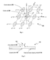
- the planar array antenna consists of identical and generally equally-spaced element antennas periodically positioned on a planar surface (the x-y plane) of the array antenna, as depicted in FIG. 1 .
- the periodicity is along two generally oblique coordinates, s 1 and s 2 , which allows us to divide the plane into similar unit cells, with the center cell abcd shown in the figure.
- FIG. 1 shows only 9 unit cells, an infinite number of cells are implied here. (Note that while a real phased array must be finite in size, in theory an array of infinite extent is often assumed.
- the infinite planar array model greatly simplifies the theoretical problem, and has been well established since its introduction four decades ago.)
- the array elements are fed by the feed and beam steering network, as depicted in the cross-sectional view of the array in FIG. 2 , to generate a selected amplitude and phase distribution in the array elements so that they form a main beam in a desired direction.
- the antenna beam is scanned or steered by variation of the phase of the elements by means of their phase shifters; thus the antenna is called a phased array.
- the CSA approach was taken by Munk and his associates (Munk, 2006; Munk and Pryor, 2002; Munk et al, 2003) and is related to several U.S. patents (U.S. Pat. No. 6,512,487 B1, 2003; U.S. Pat. No. 6,771,221 B2, 2004; U.S. Pat. No. 6,876,336 B2, 2005).
- the CSA is based on the use of planar dipoles as the array element antennas, having a ground plane spaced less than 0.5-wavelength at the highest operating frequency. Their CSA claims a 10:1 bandwidth, yet has only disclosed scant data to support it. Also, a slot-version of CSA has been pursued by Lee and his associates (J. J. Lee, 2007) with a claim of 4:1 bandwidth.
- the FA has been reported by Friedrich and his associates (Friedrich et al, 2001; Pringle et al, 2001), and has a U.S. patent (U.S. Pat. No. 6,323,809 B1, 2001).
- the FA employs a multilayer structure with real-time reconfiguration to realize a set of radiating elements and a ground conducting plane generally spaced 1 ⁇ 4-wavelength therefrom for the particular operating frequency of interest.
- the FA approach relies on design optimization processes to generate an optimum array design. Claiming a wide operating bandwidth much more than 10:1, the FA approach has insufficient supporting data in the open literature.
- the present invention is a planar broadband phased array antenna capable of wide-angle beam scan. It comprises an array of planar broadband traveling-wave (TW) antenna elements positioned parallel to a conducting ground plane spaced less than 0.5 wavelength therefrom at the highest operating frequency, and more than 0.01 wavelength at the lowest operating frequency.
- TW traveling-wave
- the array is preferably thin, and sometimes flexible and conformable to a surface that may not be strictly flat.
- the conducting ground plane ensures that the planar array antenna radiates only to the hemisphere on one side of the array, and is also part of the structure that supports the propagation of a TW along the plane of the array.
- Each planar TW antenna element is a planar 2-D frequency-independent (FI) antenna truncated to fit the unit cell of the phased array.
- the planar FI antenna as discussed in the literature (DuHamel and Scherer, 1993; Mayes, 1988; Y. Mushiake, 2004), can be a log-periodic (LP) type, the self-complementary (SC) type, the sinuous type, etc.
- the feed portion of each TW antenna element comprises two pairs of transmission lines to support dual-orthogonal or circular polarization.
- Each TW antenna element comprises a medial feed portion and radiates in the direction normal to the ground plane.
- the spacing between centers of adjacent array elements be less than 1 ⁇ 2-wavelength at the highest operating frequency. Consequently, a phased array of ultrawide bandwidth is a densely packed array. Adjacent antenna elements are arranged to be intensely coupled or connected with each other.
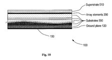
- One or more layers of dielectric or magneto-dielectric substrates can be placed between the planar TW antenna elements and the ground plane, or as superstrate placed above the TW antenna elements, or both, for enhancement of specific performances.
- FIG. 1 is a top view of a planar array of periodic elements
- FIG. 2 is a cross-sectional view of a planar array of periodic elements in FIG. 1 ;
- FIG. 3 is a top view of a planar array of 2-D LP traveling-wave element antennas
- FIG. 4 is a side cross-sectional view of the array in FIG. 3 around its center element
- FIG. 5 is a top view of the array in FIG. 3 around its center element having four feed points;
- FIG. 6 Is a top view of a center element LP TW antenna having two feed points
- FIGS. 7A-7E are drawings showing five types of frequency-independent elements
- FIG. 8A is representation of planar array of FIG. 1 for the half-space above the array by an equivalent magnetic current backed by a conductor;
- FIG. 8B is representation of planar array of FIG. 1 for the half-space above the array by an equivalent magnetic current
- FIG. 9 is an equivalent circuit at the array element feed terminals for the array of FIGS. 1 and 2 ;
- FIG. 10 is a cross-sectional view of planar array with layers of dielectric or magneto-dielectric superstrates and substrates.
- a planar array antenna 100 is perpendicular to the axis z labeled 123 .
- Array antenna 100 consists of an array of identical and generally equal-spaced traveling-wave (TW) element antennas, which are collectively labeled 200 .
- the array element antennas 200 is a thin planar array structure backed by a conducting ground plane 120 and fed by beam-steering network 150 .
- Individual array element antennas, such as the center element 250 are periodically positioned on a planar surface (the x-y plane) of the array antenna perpendicular to the z-axis 123 .
- the periodicity is along two generally oblique coordinates, s 1 and s 2 , which allows us to divide the planar array into similar unit cells, such as the central cell 280 marked by the parallelogram abcd.
- Each unit cell such as the center cell 280 , contains a physical element antenna, such as the corresponding center element 250 , as shown in FIG. 1 .
- the TW array elements are identical two-dimensional (2-D) structures in the x-y plane, which are spaced more than 0.01 wavelength and less than 0.5 wavelengths away from a parallel conducting ground plane 120 in order to support a desired dominant mode of TW in the array structure and suppress higher-order modes of TW.
- Array elements 200 are thin planar structures fed individually by the feed and beam steering network 150 , as depicted in the cross-sectional view of the array in FIG. 2 .
- the conducting part of the array elements 200 is very thin, generally much less than 1 mm in thickness, but must be thicker than the skin depth for the operating frequencies.
- the resulting electric and magnetic currents in the array elements as source currents, generate a main radiation beam in the far field in a desired direction dictated by the amplitude and phase distribution of the source currents.
- the antenna beam is scanned or steered by varying the phases of the array elements by means of their phase shifters.
- FIGS. 3 and 4 show, respectively, a top view and a cross-sectional view cut through the x-z plane for the first embodiment of the present invention, which employs planar 2-D TW element antennas, forming a broadband planar array elements 200 .
- the entire planar array consists of unit cells which are structurally similar and connected with one another.
- the centers of adjacent antenna elements, or array cells, are spaced less than 0.5 wavelengths apart for suppression of the undesirable grating lobes.
- the centers of adjacent antenna elements are also spaced more than 0.1 wavelength at the lowest operating frequency to minimize power dissipated into adjacent feeds, since they are electrically coupled or connected with each other.
- center TW element 250 which is connected with adjacent TW elements 251 , 252 , 253 , and 254 , as shown in FIGS. 3 and 5 .
- All the individual units in array elements 200 such as elements 250 , 251 , 252 , 253 , and 254 , are structurally similar, and are each defined by a unit cell as shown in FIGS. 1 and 5 . Since the adjacent elements are connected here, each array element coincides with its unit cell.
- the center unit cell 280 which is the planar region within abcd, coincides with the array center element 250 , as depicted in FIGS. 1 and 5 .
- the unit cell abcd in FIG. 5 has four similar LP (log periodic) sub-elements joining at the center of the cell.
- the TW antenna element 250 comprises a medial cluster of four terminal feed points, 250 a , 250 b , 250 c , and 250 d , which are connected to the feed and beam-steering network 150 via a feed 220 .
- the feed and beam-steering network 150 is then connected to a transceiver and beam-steering computer.
- a TW 160 generated at the feed cluster propagates along the planar array 200 , and radiates into the free space with a main beam directed at an angle above the array plane as dictated by the phase distribution in array elements 200 .
- Each TW antenna element is a planar frequency-independent (FI) antenna, as has been extensively defined and covered in the literature (DuHamel, H. D. and J. P. Scherer, 1993; Mayes, P. E., 1988). Each FI element antenna is truncated to fit into the unit cell of the phased array.
- the FI planar antenna can be a log-periodic (LP) type (as displayed in FIG. 3 ), the self-complementary (SC) type, or the sinuous type, etc.
- the feed portion of each TW antenna element as shown in FIG. 5 , comprises a cluster of four terminals, which are connected with the feed network 150 below the ground plane 120 via two pairs of transmission-line feeds 220 .
- the feed 220 has two pairs of balanced transmission lines, which are connected with the center element 250 at their two pairs of feed points, ( 250 a , 250 c ) and ( 250 b , 250 d ), respectively.
- the feed 220 consists of two balanced transmission lines of the twin-lead type.
- the two pairs of feed points, ( 250 a , 250 c ) and ( 250 b , 250 d ), are orthogonal to each other so that they can support dual-orthogonal polarization for the array element antenna 250 if the signals are processed separately, or a linear, elliptical, or circular polarization if the signals are combined with an appropriate phase relationship between.
- the two signals at the orthogonal pairs of feed points, ( 250 a , 250 c ) and ( 250 b , 250 d ) must be equal in amplitude and have a phase difference of 90°.
- the polarization of the combined radiated signal of this element antenna will be elliptical or linear.
- the sense of the circular polarization, or elliptical polarization, will depend on which pair of feeds leads in phase, and will be either right-hand or left-hand.
- the transmission-line feeds 220 and feed and beam-steering network 150 are designed to match the broadband impedance of the planar FI array elements 200 , which has been established by the analysis on complementary multiterminal planar structures without the ground plane 120 (Deschamps, 1959).
- General techniques for broadband impedance matching can be found in the book by Matthaei et al (1964, reprinted 1980).
- FIG. 6 shows a TW element 350 , which is enclosed in the unit cell 380 as marked by the rectangle abcd in a planar TW array 300 .
- the TW element 350 has a cluster of two feed terminals, 350 a and 350 b , which are fed with a signal from the output of a balun feed 220 shown in FIG. 4 .
- the balun is a device that matches between an unbalanced transmission line and a balanced transmission line. It serves the dual functions of impedance matching and transformation of the transmission lines between balanced and unbalanced modes.
- the balanced transmission line output of the balun is connected with the antenna input terminals, 350 a and 350 b ; and the unbalanced transmission line output is connected with the feed and beam-steering network 150 which generally is in an unbalanced transmission line mode such as microstrip line, coaxial cable, etc.
- feed terminal pair 350 a and 350 b generate a TW of a linear polarization in element 300 due to the structural symmetry and source excitation.
- the linear-polarization case of 350 is simpler to describe than the element 250 which can support dual-orthogonal polarization or circular polarization, but it is not as broadband since it is not close to a self-complementary antenna, even though it is of the FI type.
- FIGS. 7A , 7 B, 7 C, 7 D and 7 E show other planar FI TW element antennas 410 , 420 , 430 , 440 , and 450 which can be employed to form planar array 200 .
- FI planar (2-D) element antennas are employed, with the adjacent elements connected or strongly coupled, to form the planar array.
- a traveling wave (TW) 160 is launched at the center of each element antenna, and emitted radially outward from the feed center of the element 250 .
- the TW is impedance matched to the TW array structure for propagation radially outward along the array surface 200 .
- the TW array structure is configured so that radiation from the TW takes place rapidly and most of the power in the TW has been radiated before reaching the feed of the adjacent elements.
- adjacent antenna elements spaced more than 0.1 wavelength, center to center, at the lowest operating frequency to minimize power dissipation into adjacent feeds, which are electrically connected, or strongly coupled, with each other.
- Adjacent antenna elements are also spaced less than 0.5 wavelengths apart in order to suppress the undesirable grating lobes.
- Impedance matching is crucial to the performance of the array, and must be achieved over the broad bandwidth from the feed and beam-steering network 150 to the feed 220 , to medial four-terminal feed cluster, 250 a , 250 b , 250 c , and 250 d , and onto the TW array structure.
- Success in broadband impedance matching is rooted in the broad bandwidth of the TW structure, which consists of the planar FI element antennas and properly positioned conducting ground plane in the present invention.
- the FI array elements 200 and the closely spaced conducting ground plane 120 form a broadband TW structure that supports a variety of broadband transmission line and waveguide modes as well as modes of broadband radiation.
- planar array antenna 100 can be represented, for its fields in the half space above the array plane (i.e., for z>0), as an equivalent magnetic current M, labeled 180 , immediately above an electric conducting plane 190 , where
- the electric conducting plane can be replaced by an identical magnetic current M.
- FIG. 8B the equivalent planar array in FIG. 8A is further reduced, for the fields in the half-space above the array, to a simpler form by combining these two magnetic current sheets into a single current sheet 2 M, labeled as 182 .
- the time-harmonic magnetic field in the far zone for the half-space above the array can be totally attributed to the equivalent magnetic current 2 M in FIG. 8B , and is given by
- H ⁇ ( r ) - j ⁇ ⁇ k ⁇ ⁇ ⁇ - j ⁇ ⁇ kr 4 ⁇ ⁇ ⁇ ⁇ r ⁇ ⁇ S ⁇ 2 ⁇ ⁇ M ⁇ ( r ′ ) ⁇ ⁇ j ⁇ ⁇ k ⁇ r ⁇ ⁇ r ′ ⁇ ⁇ ⁇ s ′ ⁇ ⁇ for ⁇ ⁇ z > 0 ( 2 )
- k 2 ⁇ / ⁇
- ⁇ is the wavelength of the TW
- ⁇ is the free-space wave impedance equal to ⁇ square root over ( ⁇ o / ⁇ o ) ⁇ or 120 ⁇ .
- the symbol ⁇ circumflex over (r) ⁇ represents a unit vector in the direction of the field position vector r.
- the electric field in the far zone in a limited region can be considered to be a plane wave, and thus is given by
- the TW array elements are of the planar FI 2-D structure which supports the desired radiation according to Eqs. (2) and (3).
- the sources, fields, and the Green's function involved here are all complex quantities. Therefore, radiation will be effective only if the integrand in Eq. (2) is substantially in phase; and the radiation must also be in an orderly manner in order to yield a useful radiation pattern. For maximum radiation desired, good impedance matching is essential.
- a useful antenna radiation pattern is directly related to its source currents. Therefore, it is advantageous to design the broadband planar array from known broadband antenna configurations, such as the TW antennas discussed here, rather than by approaches starting with a narrowband antenna or unknown design and then trying to broadband it.
- the active element impedance Z T can be represented as a parallel combination of an impedance Z A , 361 , for the array elements 200 in the presence of the ground plane 120 , plus an impedance Z TW , 362 , for the transmission lines formed by the TW array structure array elements 200 .
- Z A , 361 and Z TW 362 For planar FI antennas and the associated TW structures, their broadband impedance property of Z A , 361 and Z TW 362 has been discussed by Wang (2000) and Wang et al (2006), which can be adapted to the present array design.
- the impedance property of Z A , 361 and Z TW 362 , as well as radiation properties such as broadening of the scan angle, can also be improved by employing layers of dielectric or magneto-dielectric substrates of various permittivity or permeability (between array elements 200 and ground plane 120 ) and superstrates (above array elements 200 ), as shown in a cross-sectional view of such a planar array in FIG. 10 .
- a breadboard 5 ⁇ 5-cell planar array similar to that in FIGS. 3-5 was designed, fabricated, and tested. Each cell has both x and y directed LP planar dipoles.
- the vertical center element has a broadband balun feed across its feed terminals (corresponding to 250 b and 250 d in FIG. 5 ).
- Each of the other 24 vertical LP dipoles has a 100-ohm resistor load. All the 25 horizontal LP dipoles have their feed terminals (corresponding to 250 a and 250 c in FIG. 5 ) floating (open-circuit with no connection to other element or device).
- the properties of a large planar array can be determined by measuring its “active element gain pattern,” which takes account of the mutual coupling and beam scan of a planar array (Mailloux, 1994; Pozar, 1994).
- the active gain pattern reveals the scan property of the element antenna, including both impedance matching and radiation pattern.
- the array gain pattern is then obtained from the active element gain pattern and the array factor.
- the active element gain pattern of centrally located elements of the array are similar, and can be measured with a small array which is fed only at the center element, with all other elements terminated in matched passive loads.
- the array is planar, it can be slightly curved, either to expand its performance features or to conform to a mounting platform.
- FIG. 10 is a cross-sectional view of such a planar array implemented with layers of dielectric or magneto-dielectric superstrates and substrates of various permittivity or permeability.
Landscapes
- Variable-Direction Aerials And Aerial Arrays (AREA)
Abstract
Description
- The present invention is generally related to radio-frequency antennas and, more particularly, broadband planar beam-scan array antennas.
- Broadband planar array antennas have become increasingly more important for both military and commercial applications. The broadband requirement is driven by the proliferation of wireless systems operating at different separate frequencies and the need for high speed. The planar form factor is desirable and often necessary for both transport and installation of the array antenna, because of the associated features of low profile and conformability to platform. The planar form also lends itself to low weight and low-cost production methods such as a printed-circuit board.
- The planar array antenna consists of identical and generally equally-spaced element antennas periodically positioned on a planar surface (the x-y plane) of the array antenna, as depicted in
FIG. 1 . The periodicity is along two generally oblique coordinates, s1 and s2, which allows us to divide the plane into similar unit cells, with the center cell abcd shown in the figure. Although the arrangement ofFIG. 1 shows only 9 unit cells, an infinite number of cells are implied here. (Note that while a real phased array must be finite in size, in theory an array of infinite extent is often assumed. The infinite planar array model greatly simplifies the theoretical problem, and has been well established since its introduction four decades ago.) - The array elements are fed by the feed and beam steering network, as depicted in the cross-sectional view of the array in
FIG. 2 , to generate a selected amplitude and phase distribution in the array elements so that they form a main beam in a desired direction. The antenna beam is scanned or steered by variation of the phase of the elements by means of their phase shifters; thus the antenna is called a phased array. Although the discussion herein is for the case of transmit, by reciprocity it applies also to the case of receive. - Although the possibility of broadband planar beam-scan array had been envisioned four decades ago (Wheeler, 1965), the design of broadband planar arrays has been mostly focused on arrays using 3-dimensional (3-D) elements such as the flared slots. 3-D elements have a large dimension perpendicular to the plane of the array (along the z axis), thus are not amenable to many low-cost production techniques. As a result, research efforts have been launched since late 1990s to explore the use of 2-dimensional (2-D) array elements, such as planar patches, flat dipoles, and slots, in planar arrays. Findings so far have shown that planar arrays of 2-D elements have the potential of wide bandwidths, large scan angle, as well as reduced thickness and weight. Since planar beam-scan arrays with 2-D elements are amenable to truly low-cost printed-circuit-board production, their potential applications in the commercial and military markets are recognized.
- Hansen (1999) showed that a planar phased array using planar dipoles, without a ground plane, exhibits easy-to-match active resistance and fairly stable element gain pattern, over a wide range of scan angles and bandwidth (over 5:1). Yet the reactance remains to be matched over the frequency. Also, since this array does not have a ground plane, it has a bidirectional radiation pattern (on both sides of the array plane). The resulting bidirectional radiation renders this planar array unsuitable for applications in which conformal mounting on a platform is required. When Hansen added a ground plane to one side of array to suppress its back radiation, he noted disruptive effects. Therefore, Hansen's array is impractical, just like Wheeler's array, until a ground plane is added.
- Following Hansen's reporting, research efforts in planar arrays soon escalated, essentially following two approaches: the Current Sheet Antenna (CSA) and the Fragmented Aperture (FA).
- The CSA approach was taken by Munk and his associates (Munk, 2006; Munk and Pryor, 2002; Munk et al, 2003) and is related to several U.S. patents (U.S. Pat. No. 6,512,487 B1, 2003; U.S. Pat. No. 6,771,221 B2, 2004; U.S. Pat. No. 6,876,336 B2, 2005). The CSA is based on the use of planar dipoles as the array element antennas, having a ground plane spaced less than 0.5-wavelength at the highest operating frequency. Their CSA claims a 10:1 bandwidth, yet has only disclosed scant data to support it. Also, a slot-version of CSA has been pursued by Lee and his associates (J. J. Lee, 2007) with a claim of 4:1 bandwidth.
- The FA has been reported by Friedrich and his associates (Friedrich et al, 2001; Pringle et al, 2001), and has a U.S. patent (U.S. Pat. No. 6,323,809 B1, 2001). The FA employs a multilayer structure with real-time reconfiguration to realize a set of radiating elements and a ground conducting plane generally spaced ¼-wavelength therefrom for the particular operating frequency of interest. The FA approach relies on design optimization processes to generate an optimum array design. Claiming a wide operating bandwidth much more than 10:1, the FA approach has insufficient supporting data in the open literature. The viability of the technique of a movable ground plane by reconfiguration, as claimed in the FA approach, was questioned categorically by Munk and Pryor (2002).
- Indeed, as observed by Thors et al (2005), design guidelines and results are often scant or nonexistent in the documents on CSA and FA. It must be emphasized that, even though extremely broad bandwidth can be easily designed for the case of planar arrays of 2-D elements with no supporting ground plane, design of broadband planar array having a ground plane is difficult. This is particularly true in the case of the FA approach, for which Thors et al only managed to achieve a bandwidth of 2.23:1.
- This inventor noted that the theory and experimentation on CSA and FA disclosed to the public often are indirect and incomplete, and have not yet realized full-fledged broadband performance as claimed. He also noted some limitations and deficiencies in certain design concepts of CSA and FA, which consist of inherently narrowband components whose bandwidths are difficult to broaden by reconfiguration or optimization. He then conceived the present invention based on the traveling-wave (TW) antenna concept, which potentially has superior performance over prior-art approaches.
- The present invention is a planar broadband phased array antenna capable of wide-angle beam scan. It comprises an array of planar broadband traveling-wave (TW) antenna elements positioned parallel to a conducting ground plane spaced less than 0.5 wavelength therefrom at the highest operating frequency, and more than 0.01 wavelength at the lowest operating frequency. The array is preferably thin, and sometimes flexible and conformable to a surface that may not be strictly flat. The conducting ground plane ensures that the planar array antenna radiates only to the hemisphere on one side of the array, and is also part of the structure that supports the propagation of a TW along the plane of the array.
- Each planar TW antenna element is a planar 2-D frequency-independent (FI) antenna truncated to fit the unit cell of the phased array. The planar FI antenna, as discussed in the literature (DuHamel and Scherer, 1993; Mayes, 1988; Y. Mushiake, 2004), can be a log-periodic (LP) type, the self-complementary (SC) type, the sinuous type, etc. The feed portion of each TW antenna element comprises two pairs of transmission lines to support dual-orthogonal or circular polarization. Each TW antenna element comprises a medial feed portion and radiates in the direction normal to the ground plane.
- To avoid the grating lobe problem, it is desirable that the spacing between centers of adjacent array elements be less than ½-wavelength at the highest operating frequency. Consequently, a phased array of ultrawide bandwidth is a densely packed array. Adjacent antenna elements are arranged to be intensely coupled or connected with each other.
- One or more layers of dielectric or magneto-dielectric substrates can be placed between the planar TW antenna elements and the ground plane, or as superstrate placed above the TW antenna elements, or both, for enhancement of specific performances.
- Many aspects of the invention can be better understood with reference to the following drawings. The components in the drawings are not necessarily to scale, emphasis instead being placed upon clearly illustrating the principles of the present invention. Moreover, in the drawings, like reference numerals designate corresponding parts throughout the several views.
-
FIG. 1 is a top view of a planar array of periodic elements; -
FIG. 2 is a cross-sectional view of a planar array of periodic elements inFIG. 1 ; -
FIG. 3 is a top view of a planar array of 2-D LP traveling-wave element antennas; -
FIG. 4 is a side cross-sectional view of the array inFIG. 3 around its center element; -
FIG. 5 is a top view of the array inFIG. 3 around its center element having four feed points; -
FIG. 6 Is a top view of a center element LP TW antenna having two feed points; -
FIGS. 7A-7E are drawings showing five types of frequency-independent elements; -
FIG. 8A is representation of planar array ofFIG. 1 for the half-space above the array by an equivalent magnetic current backed by a conductor; -
FIG. 8B is representation of planar array ofFIG. 1 for the half-space above the array by an equivalent magnetic current; -
FIG. 9 is an equivalent circuit at the array element feed terminals for the array ofFIGS. 1 and 2 ; and -
FIG. 10 is a cross-sectional view of planar array with layers of dielectric or magneto-dielectric superstrates and substrates. - As depicted in the top view in
FIG. 1 and a cross-sectional view inFIG. 2 , aplanar array antenna 100 is perpendicular to the axis z labeled 123.Array antenna 100 consists of an array of identical and generally equal-spaced traveling-wave (TW) element antennas, which are collectively labeled 200. Thearray element antennas 200 is a thin planar array structure backed by a conductingground plane 120 and fed by beam-steering network 150. Individual array element antennas, such as thecenter element 250, are periodically positioned on a planar surface (the x-y plane) of the array antenna perpendicular to the z-axis 123. The periodicity is along two generally oblique coordinates, s1 and s2, which allows us to divide the planar array into similar unit cells, such as thecentral cell 280 marked by the parallelogram abcd. Each unit cell, such as thecenter cell 280, contains a physical element antenna, such as thecorresponding center element 250, as shown inFIG. 1 . When x=s1 and y=s2, the unit cells become square or rectangular in shape. - A rigorous theory has been developed for planar arrays of infinite extent, which are amenable to analyses by expansions of Floquet modes. In an infinite planar array, the radiation characteristics of any element, or unit cell, are similar to those of the
center element 250 orcenter cell 280, respectively. In experimentation, arrays are of course of finite dimensions; yet most of the elements in an array are not close to the edge and thus can be considered to be in an array environment of infinite extent. Analyses and measurements on finite arrays have validated this theory of infinite planar array, which is further supplemented by treating the elements near the edge of a planar array in a refined design approach. The details will be further discussed in a later section on the theory of this invention. - The TW array elements, collectively labeled 200, are identical two-dimensional (2-D) structures in the x-y plane, which are spaced more than 0.01 wavelength and less than 0.5 wavelengths away from a parallel
conducting ground plane 120 in order to support a desired dominant mode of TW in the array structure and suppress higher-order modes of TW.Array elements 200 are thin planar structures fed individually by the feed andbeam steering network 150, as depicted in the cross-sectional view of the array inFIG. 2 . The conducting part of thearray elements 200 is very thin, generally much less than 1 mm in thickness, but must be thicker than the skin depth for the operating frequencies. The resulting electric and magnetic currents in the array elements, as source currents, generate a main radiation beam in the far field in a desired direction dictated by the amplitude and phase distribution of the source currents. As a phased array, the antenna beam is scanned or steered by varying the phases of the array elements by means of their phase shifters. -
FIGS. 3 and 4 show, respectively, a top view and a cross-sectional view cut through the x-z plane for the first embodiment of the present invention, which employs planar 2-D TW element antennas, forming a broadbandplanar array elements 200. The entire planar array consists of unit cells which are structurally similar and connected with one another. The centers of adjacent antenna elements, or array cells, are spaced less than 0.5 wavelengths apart for suppression of the undesirable grating lobes. The centers of adjacent antenna elements are also spaced more than 0.1 wavelength at the lowest operating frequency to minimize power dissipated into adjacent feeds, since they are electrically coupled or connected with each other. - Let us first focus on the
center TW element 250, which is connected withadjacent TW elements FIGS. 3 and 5 . All the individual units inarray elements 200, such aselements FIGS. 1 and 5 . Since the adjacent elements are connected here, each array element coincides with its unit cell. For example, thecenter unit cell 280, which is the planar region within abcd, coincides with thearray center element 250, as depicted inFIGS. 1 and 5 . - The unit cell abcd in
FIG. 5 has four similar LP (log periodic) sub-elements joining at the center of the cell. TheTW antenna element 250 comprises a medial cluster of four terminal feed points, 250 a, 250 b, 250 c, and 250 d, which are connected to the feed and beam-steering network 150 via afeed 220. The feed and beam-steering network 150 is then connected to a transceiver and beam-steering computer. ATW 160 generated at the feed cluster propagates along theplanar array 200, and radiates into the free space with a main beam directed at an angle above the array plane as dictated by the phase distribution inarray elements 200. Although the discussion here is for the case of transmit, by reciprocity it applies also to the case of receive. - Each TW antenna element is a planar frequency-independent (FI) antenna, as has been extensively defined and covered in the literature (DuHamel, H. D. and J. P. Scherer, 1993; Mayes, P. E., 1988). Each FI element antenna is truncated to fit into the unit cell of the phased array. The FI planar antenna can be a log-periodic (LP) type (as displayed in
FIG. 3 ), the self-complementary (SC) type, or the sinuous type, etc. The feed portion of each TW antenna element, as shown inFIG. 5 , comprises a cluster of four terminals, which are connected with thefeed network 150 below theground plane 120 via two pairs of transmission-line feeds 220. Thefeed 220 has two pairs of balanced transmission lines, which are connected with thecenter element 250 at their two pairs of feed points, (250 a, 250 c) and (250 b, 250 d), respectively. - The
feed 220 consists of two balanced transmission lines of the twin-lead type. The two pairs of feed points, (250 a, 250 c) and (250 b, 250 d), are orthogonal to each other so that they can support dual-orthogonal polarization for thearray element antenna 250 if the signals are processed separately, or a linear, elliptical, or circular polarization if the signals are combined with an appropriate phase relationship between. For circular polarization, the two signals at the orthogonal pairs of feed points, (250 a, 250 c) and (250 b, 250 d), must be equal in amplitude and have a phase difference of 90°. For other amplitude and phase differences between the two signals at the pair of feed points, the polarization of the combined radiated signal of this element antenna will be elliptical or linear. The sense of the circular polarization, or elliptical polarization, will depend on which pair of feeds leads in phase, and will be either right-hand or left-hand. - The transmission-line feeds 220 and feed and beam-
steering network 150 are designed to match the broadband impedance of the planarFI array elements 200, which has been established by the analysis on complementary multiterminal planar structures without the ground plane 120 (Deschamps, 1959). General techniques for broadband impedance matching can be found in the book by Matthaei et al (1964, reprinted 1980). - As a variation,
FIG. 6 shows aTW element 350, which is enclosed in theunit cell 380 as marked by the rectangle abcd in aplanar TW array 300. TheTW element 350 has a cluster of two feed terminals, 350 a and 350 b, which are fed with a signal from the output of abalun feed 220 shown inFIG. 4 . The balun is a device that matches between an unbalanced transmission line and a balanced transmission line. It serves the dual functions of impedance matching and transformation of the transmission lines between balanced and unbalanced modes. In the present case, the balanced transmission line output of the balun is connected with the antenna input terminals, 350 a and 350 b; and the unbalanced transmission line output is connected with the feed and beam-steering network 150 which generally is in an unbalanced transmission line mode such as microstrip line, coaxial cable, etc. InFIG. 6 , feedterminal pair element 300 due to the structural symmetry and source excitation. The linear-polarization case of 350 is simpler to describe than theelement 250 which can support dual-orthogonal polarization or circular polarization, but it is not as broadband since it is not close to a self-complementary antenna, even though it is of the FI type. -
FIGS. 7A , 7B, 7C, 7D and 7E show other planar FITW element antennas planar array 200. - It is noted that prior-art approaches for broadband planar arrays either use narrowband dipole/slot as building blocks, or relying on reconfiguration during operation, to achieve broadband. In the present invention, frequency-independent (FI) planar (2-D) element antennas are employed, with the adjacent elements connected or strongly coupled, to form the planar array.
- Without loss of generality, the theory of operation can be explained by considering the case of transmit; the case of receive is similar on the basis of the principle of reciprocity. Referring to
FIGS. 4 and 5 , a traveling wave (TW) 160 is launched at the center of each element antenna, and emitted radially outward from the feed center of theelement 250. The TW is impedance matched to the TW array structure for propagation radially outward along thearray surface 200. In addition, the TW array structure is configured so that radiation from the TW takes place rapidly and most of the power in the TW has been radiated before reaching the feed of the adjacent elements. The rapidity and efficiency of the radiation is also facilitated by having adjacent antenna elements spaced more than 0.1 wavelength, center to center, at the lowest operating frequency to minimize power dissipation into adjacent feeds, which are electrically connected, or strongly coupled, with each other. Adjacent antenna elements are also spaced less than 0.5 wavelengths apart in order to suppress the undesirable grating lobes. - Impedance matching is crucial to the performance of the array, and must be achieved over the broad bandwidth from the feed and beam-
steering network 150 to thefeed 220, to medial four-terminal feed cluster, 250 a, 250 b, 250 c, and 250 d, and onto the TW array structure. Success in broadband impedance matching is rooted in the broad bandwidth of the TW structure, which consists of the planar FI element antennas and properly positioned conducting ground plane in the present invention. TheFI array elements 200 and the closely spaced conductingground plane 120 form a broadband TW structure that supports a variety of broadband transmission line and waveguide modes as well as modes of broadband radiation. - The theoretical foundation supporting the present invention can be found in the literature. A rigorous treatment on the basic theory and numerical analysis of planar arrays can be found in Wang (1991) and Mailloux (1994). Discussions on the traveling-wave antennas in general can be found in Walter (1965). General impedance matching techniques for multi-stage transmission lines and waveguides are in the literature (e.g., Matthaei et al, 1964, reprinted 1985).
- The radiation of the present broadband planar TW array is discussed as follows. The basic physics of the planar TW array is largely similar to that of the broadband planer TW antennas discussed in Wang (2000) and Wang et al (2006). By invoking the equivalence principle and image theory, as shown in
FIG. 8A , theplanar array antenna 100 can be represented, for its fields in the half space above the array plane (i.e., for z>0), as an equivalent magnetic current M, labeled 180, immediately above anelectric conducting plane 190, where -
M=−n×E=−{circumflex over (z)}×E (1) - And E is the electric field on the planar surface of the array at z=0.
- Note here that the conducting
plane 190, as shown inFIG. 8A , is not thesame ground plane 120; rather, it is a fictitious conducting plane positioned immediately below, and infinitesimally close to, the array surface at z=0, namely, at z=0−. Note also that only the “slot” part of the array has a non-vanishing magnetic current M since the tangential E fields on a perfectly conducting surface, such as the conducting part of the array elements, must vanish. Therefore, the magnetic current M=−n×E exists only on the slot aperture of the array elements. - By invoking the image theorem, the electric conducting plane can be replaced by an identical magnetic current M. In
FIG. 8B , the equivalent planar array inFIG. 8A is further reduced, for the fields in the half-space above the array, to a simpler form by combining these two magnetic current sheets into a singlecurrent sheet 2M, labeled as 182. - The time-harmonic magnetic field in the far zone for the half-space above the array can be totally attributed to the equivalent magnetic current 2M in
FIG. 8B , and is given by -
- where k=2π/λ, λ is the wavelength of the TW, and η is the free-space wave impedance equal to √{square root over (μo/∈o)} or 120π. The primed and unprimed position vectors, r and r′, with magnitudes r and r′, respectively, refer to field and source points, respectively, in the source and field coordinates. (All the “primed” symbols refer to the source.) The symbol {circumflex over (r)} represents a unit vector in the direction of the field position vector r. S is the plane at z=0. The electric field in the far zone in a limited region can be considered to be a plane wave, and thus is given by
-
E(r)=−η{circumflex over (r)}×H for z>0 (3) - Now, the TW array elements are of the planar FI 2-D structure which supports the desired radiation according to Eqs. (2) and (3). Note here that the sources, fields, and the Green's function involved here are all complex quantities. Therefore, radiation will be effective only if the integrand in Eq. (2) is substantially in phase; and the radiation must also be in an orderly manner in order to yield a useful radiation pattern. For maximum radiation desired, good impedance matching is essential. Based on antenna theory, and specialized to the present problem in Eqs. (2) and (3), a useful antenna radiation pattern is directly related to its source currents. Therefore, it is advantageous to design the broadband planar array from known broadband antenna configurations, such as the TW antennas discussed here, rather than by approaches starting with a narrowband antenna or unknown design and then trying to broadband it.
- For impedance matching, an equivalent circuit for the TW array structure, at the array element feed terminals and looking outward to
array elements 200, is shown inFIG. 9 . At the arrayelement feed terminals 360 a and 360 b, the active element impedance ZT, labeled 360, can be represented as a parallel combination of an impedance ZA, 361, for thearray elements 200 in the presence of theground plane 120, plus an impedance ZTW, 362, for the transmission lines formed by the TW arraystructure array elements 200. For planar FI antennas and the associated TW structures, their broadband impedance property of ZA, 361 andZ TW 362 has been discussed by Wang (2000) and Wang et al (2006), which can be adapted to the present array design. - The impedance property of ZA, 361 and
Z TW 362, as well as radiation properties such as broadening of the scan angle, can also be improved by employing layers of dielectric or magneto-dielectric substrates of various permittivity or permeability (betweenarray elements 200 and ground plane 120) and superstrates (above array elements 200), as shown in a cross-sectional view of such a planar array inFIG. 10 . - Further impedance matching can of course be achieved in the feed and beam-
steering network 150. - Basic experimentation has been performed for this invention. A breadboard 5×5-cell planar array similar to that in
FIGS. 3-5 was designed, fabricated, and tested. Each cell has both x and y directed LP planar dipoles. The vertical center element has a broadband balun feed across its feed terminals (corresponding to 250 b and 250 d inFIG. 5 ). Each of the other 24 vertical LP dipoles has a 100-ohm resistor load. All the 25 horizontal LP dipoles have their feed terminals (corresponding to 250 a and 250 c inFIG. 5 ) floating (open-circuit with no connection to other element or device). - According to the theory and practices in planar arrays, the properties of a large planar array can be determined by measuring its “active element gain pattern,” which takes account of the mutual coupling and beam scan of a planar array (Mailloux, 1994; Pozar, 1994). The active gain pattern reveals the scan property of the element antenna, including both impedance matching and radiation pattern. The array gain pattern is then obtained from the active element gain pattern and the array factor. The active element gain pattern of centrally located elements of the array are similar, and can be measured with a small array which is fed only at the center element, with all other elements terminated in matched passive loads.
- Measurements on the impedance and active gain pattern of the model indicate that this array has a 10:1 bandwidth potential. Another breadboard planar array model empirically studied, showing broadband potential, was a 113-element array with unit elements of the type shown in
FIG. 7E . - Although adjacent array elements shown are directly connected electrically, the direct connection can be replaced with indirect, yet strong, coupling for certain performance features or to adapt to particular element antenna configurations.
- Although the array is planar, it can be slightly curved, either to expand its performance features or to conform to a mounting platform.
- Layers of dielectric or magneto-dielectric substrates (between
array elements 200 and ground plane 120) and superstrates (above array elements 200) can be used to improve the performance and broaden its frequency bandwidth and scan angle.FIG. 10 is a cross-sectional view of such a planar array implemented with layers of dielectric or magneto-dielectric superstrates and substrates of various permittivity or permeability.
Claims (12)
Priority Applications (2)
| Application Number | Priority Date | Filing Date | Title |
|---|---|---|---|
| US11/831,002 US8264410B1 (en) | 2007-07-31 | 2007-07-31 | Planar broadband traveling-wave beam-scan array antennas |
| CN200810144442.8A CN101359777B (en) | 2007-07-31 | 2008-07-31 | Planar broad band travelling wave beam scanning array antenna |
Applications Claiming Priority (1)
| Application Number | Priority Date | Filing Date | Title |
|---|---|---|---|
| US11/831,002 US8264410B1 (en) | 2007-07-31 | 2007-07-31 | Planar broadband traveling-wave beam-scan array antennas |
Publications (2)
| Publication Number | Publication Date |
|---|---|
| US8264410B1 US8264410B1 (en) | 2012-09-11 |
| US20120249374A1 true US20120249374A1 (en) | 2012-10-04 |
Family
ID=40332158
Family Applications (1)
| Application Number | Title | Priority Date | Filing Date |
|---|---|---|---|
| US11/831,002 Active 2030-11-09 US8264410B1 (en) | 2007-07-31 | 2007-07-31 | Planar broadband traveling-wave beam-scan array antennas |
Country Status (2)
| Country | Link |
|---|---|
| US (1) | US8264410B1 (en) |
| CN (1) | CN101359777B (en) |
Cited By (13)
| Publication number | Priority date | Publication date | Assignee | Title |
|---|---|---|---|---|
| US20090102705A1 (en) * | 2006-11-30 | 2009-04-23 | Obermeyer Henry K | Spectrometric synthetic aperture radar |
| US20140374616A1 (en) * | 2013-06-24 | 2014-12-25 | Raytheon Company | Imaging Antenna and Related Techniques |
| JP2015162682A (en) * | 2014-02-25 | 2015-09-07 | 日本電信電話株式会社 | Antenna, base station device, and arrangement method of antenna elements |
| US10439281B2 (en) | 2015-10-29 | 2019-10-08 | Commscope Technologies Llc | Calibrated circuit boards and related integrated antenna systems having enhanced inter-band isolation |
| US10439283B2 (en) | 2014-12-12 | 2019-10-08 | Huawei Technologies Co., Ltd. | High coverage antenna array and method using grating lobe layers |
| WO2020041598A1 (en) * | 2018-08-24 | 2020-02-27 | Searete Llc | Waveguide- and cavity-backed antenna arrays with distributed signal amplifiers for transmission of a high-power beam |
| US10673139B2 (en) | 2015-06-29 | 2020-06-02 | Huawei Technologies Co., Ltd. | Phased array system and beam scanning method |
| CN113506988A (en) * | 2021-06-29 | 2021-10-15 | 华南理工大学 | Millimeter-wave wide-angle scanning phased array antenna based on unit beam heterogeneity |
| US11271300B2 (en) * | 2018-08-24 | 2022-03-08 | Searete Llc | Cavity-backed antenna array with distributed signal amplifiers for transmission of a high-power beam |
| US11316280B2 (en) | 2014-06-06 | 2022-04-26 | Rockwell Collins, Inc. | Tiling system and method for an array antenna |
| US11355841B2 (en) * | 2018-08-24 | 2022-06-07 | Searete Llc | Waveguide-backed antenna array with distributed signal amplifiers for transmission of a high-power beam |
| WO2022250428A1 (en) * | 2021-05-24 | 2022-12-01 | 삼성전자 주식회사 | Antenna and electronic device comprising same |
| US20240380125A1 (en) * | 2021-08-30 | 2024-11-14 | Aeterlink Corp. | Multi-antenna arrangement and its connecting method |
Families Citing this family (20)
| Publication number | Priority date | Publication date | Assignee | Title |
|---|---|---|---|---|
| US9379438B1 (en) * | 2009-12-01 | 2016-06-28 | Viasat, Inc. | Fragmented aperture for the Ka/K/Ku frequency bands |
| US8497808B2 (en) * | 2011-04-08 | 2013-07-30 | Wang Electro-Opto Corporation | Ultra-wideband miniaturized omnidirectional antennas via multi-mode three-dimensional (3-D) traveling-wave (TW) |
| TWD160060S (en) * | 2013-05-17 | 2014-04-21 | 樂榮工業股份有限公司 | Antenna Part |
| GB2542163B (en) * | 2015-09-10 | 2021-07-07 | Stratospheric Platforms Ltd | Lightweight process and apparatus for communicating with user antenna phased arrays |
| TWI667842B (en) * | 2016-04-15 | 2019-08-01 | 和碩聯合科技股份有限公司 | Antenna system and control method |
| EP3526855B1 (en) * | 2016-10-17 | 2026-01-14 | Director General, Defence Research & Development Organisation (DRDO) | Single layer shared aperture dual band antenna |
| CN106785487A (en) * | 2017-01-10 | 2017-05-31 | 成都北斗天线工程技术有限公司 | A kind of active impedance matching process of close coupling antenna array |
| CN109256614B (en) * | 2017-07-12 | 2020-04-21 | 中国移动通信集团公司 | An antenna and communication equipment |
| US10992049B2 (en) * | 2018-02-23 | 2021-04-27 | Nokia Shanghai Bell Co., Ltd. | Elliptically polarized cavity backed wideband slot antenna |
| WO2020028363A1 (en) * | 2018-07-31 | 2020-02-06 | Quintel Cayman Limited | Split diamond antenna element for controlling azimuth pattern in different array configurations |
| CN109524771B (en) * | 2018-11-28 | 2022-09-27 | 哈尔滨工业大学(威海) | Dual-polarized sine antenna device based on GCPW feed |
| KR102533885B1 (en) * | 2019-05-31 | 2023-05-18 | 가부시키가이샤 무라타 세이사쿠쇼 | Sub-array antenna, array antenna, antenna module and communication device |
| CN112363542B (en) * | 2020-11-23 | 2022-09-27 | 上海航天测控通信研究所 | Ground equipment for rocket-borne phased array antenna initial phase balancing |
| CN112701471B (en) * | 2020-11-27 | 2022-06-03 | 电子科技大学 | All-dielectric integrated ultra-wideband low-profile polymorphic conformal phased array antenna |
| CN112542685B (en) * | 2020-12-18 | 2021-11-02 | 北京大学 | A microwave and terahertz wave all-metal hyperbolic metamaterial antenna and its realization method |
| CN112768922B (en) * | 2020-12-29 | 2022-06-10 | 中山大学 | A 2×4 Broadband Beam Fixed Traveling-Wave Antenna |
| CN112563764B (en) * | 2021-02-19 | 2021-05-14 | 成都天锐星通科技有限公司 | Antenna design method and device and electronic equipment |
| CN113219244B (en) * | 2021-05-07 | 2022-08-30 | 北京航空航天大学 | Ultra-wide band plane wave generating system |
| CN117795778A (en) * | 2021-08-31 | 2024-03-29 | 3M创新有限公司 | Antenna Assemblies and Communication Systems |
| CN119647099B (en) * | 2024-11-26 | 2025-12-09 | 北京航空航天大学 | Rapid modeling method for near-field radiation characteristics of electric scanning array |
Family Cites Families (21)
| Publication number | Priority date | Publication date | Assignee | Title |
|---|---|---|---|---|
| US5313216A (en) | 1991-05-03 | 1994-05-17 | Georgia Tech Research Corporation | Multioctave microstrip antenna |
| US5274390A (en) * | 1991-12-06 | 1993-12-28 | The Pennsylvania Research Corporation | Frequency-Independent phased-array antenna |
| US5483248A (en) * | 1993-08-10 | 1996-01-09 | Hughes Aircraft Company | Continuous transverse stub element devices for flat plate antenna arrays |
| US5508710A (en) | 1994-03-11 | 1996-04-16 | Wang-Tripp Corporation | Conformal multifunction shared-aperture antenna |
| US5621422A (en) | 1994-08-22 | 1997-04-15 | Wang-Tripp Corporation | Spiral-mode microstrip (SMM) antennas and associated methods for exciting, extracting and multiplexing the various spiral modes |
| US5936595A (en) | 1997-05-15 | 1999-08-10 | Wang Electro-Opto Corporation | Integrated antenna phase shifter |
| US6094172A (en) * | 1998-07-30 | 2000-07-25 | The United States Of America As Represented By The Secretary Of The Army | High performance traveling wave antenna for microwave and millimeter wave applications |
| US6137453A (en) | 1998-11-19 | 2000-10-24 | Wang Electro-Opto Corporation | Broadband miniaturized slow-wave antenna |
| US6323809B1 (en) | 1999-05-28 | 2001-11-27 | Georgia Tech Research Corporation | Fragmented aperture antennas and broadband antenna ground planes |
| US6512487B1 (en) | 2000-10-31 | 2003-01-28 | Harris Corporation | Wideband phased array antenna and associated methods |
| WO2003034545A1 (en) * | 2001-10-16 | 2003-04-24 | Fractus, S.A. | Multifrequency microstrip patch antenna with parasitic coupled elements |
| US6771221B2 (en) | 2002-01-17 | 2004-08-03 | Harris Corporation | Enhanced bandwidth dual layer current sheet antenna |
| US7705782B2 (en) * | 2002-10-23 | 2010-04-27 | Southern Methodist University | Microstrip array antenna |
| US6972729B2 (en) * | 2003-06-20 | 2005-12-06 | Wang Electro-Opto Corporation | Broadband/multi-band circular array antenna |
| US6876336B2 (en) | 2003-08-04 | 2005-04-05 | Harris Corporation | Phased array antenna with edge elements and associated methods |
| CN1677749B (en) * | 2004-03-29 | 2012-04-18 | 王氏电-光公司 | Broadband/multi-band circular array antenna |
| US7250908B2 (en) * | 2004-05-15 | 2007-07-31 | Southern Methodist University | Beam steering array antenna method and apparatus |
| WO2005114784A1 (en) * | 2004-05-21 | 2005-12-01 | Telefonaktiebolaget Lm Ericsson (Publ) | Broadband array antennas using complementary antenna |
| EP1754281B1 (en) * | 2004-06-10 | 2012-10-03 | TELEFONAKTIEBOLAGET LM ERICSSON (publ) | Patch antenna |
| JPWO2006059568A1 (en) * | 2004-11-30 | 2008-06-05 | 松下電器産業株式会社 | Antenna device |
| US20070159396A1 (en) * | 2006-01-06 | 2007-07-12 | Sievenpiper Daniel F | Antenna structures having adjustable radiation characteristics |
-
2007
- 2007-07-31 US US11/831,002 patent/US8264410B1/en active Active
-
2008
- 2008-07-31 CN CN200810144442.8A patent/CN101359777B/en active Active
Cited By (18)
| Publication number | Priority date | Publication date | Assignee | Title |
|---|---|---|---|---|
| US20090102705A1 (en) * | 2006-11-30 | 2009-04-23 | Obermeyer Henry K | Spectrometric synthetic aperture radar |
| US9019143B2 (en) * | 2006-11-30 | 2015-04-28 | Henry K. Obermeyer | Spectrometric synthetic aperture radar |
| US20140374616A1 (en) * | 2013-06-24 | 2014-12-25 | Raytheon Company | Imaging Antenna and Related Techniques |
| US9329255B2 (en) * | 2013-06-24 | 2016-05-03 | Raytheon Company | Imaging antenna and related techniques |
| JP2016529771A (en) * | 2013-06-24 | 2016-09-23 | レイセオン カンパニー | Imaging log periodic antenna with stepped balun and related techniques |
| TWI587576B (en) * | 2013-06-24 | 2017-06-11 | 雷森公司 | Imaging antenna and related techniques |
| JP2015162682A (en) * | 2014-02-25 | 2015-09-07 | 日本電信電話株式会社 | Antenna, base station device, and arrangement method of antenna elements |
| US11316280B2 (en) | 2014-06-06 | 2022-04-26 | Rockwell Collins, Inc. | Tiling system and method for an array antenna |
| US10439283B2 (en) | 2014-12-12 | 2019-10-08 | Huawei Technologies Co., Ltd. | High coverage antenna array and method using grating lobe layers |
| US10673139B2 (en) | 2015-06-29 | 2020-06-02 | Huawei Technologies Co., Ltd. | Phased array system and beam scanning method |
| US10439281B2 (en) | 2015-10-29 | 2019-10-08 | Commscope Technologies Llc | Calibrated circuit boards and related integrated antenna systems having enhanced inter-band isolation |
| WO2020041598A1 (en) * | 2018-08-24 | 2020-02-27 | Searete Llc | Waveguide- and cavity-backed antenna arrays with distributed signal amplifiers for transmission of a high-power beam |
| US11271300B2 (en) * | 2018-08-24 | 2022-03-08 | Searete Llc | Cavity-backed antenna array with distributed signal amplifiers for transmission of a high-power beam |
| US11355841B2 (en) * | 2018-08-24 | 2022-06-07 | Searete Llc | Waveguide-backed antenna array with distributed signal amplifiers for transmission of a high-power beam |
| WO2022250428A1 (en) * | 2021-05-24 | 2022-12-01 | 삼성전자 주식회사 | Antenna and electronic device comprising same |
| US12444859B2 (en) | 2021-05-24 | 2025-10-14 | Samsung Electronics Co., Ltd. | Antenna and electronic device including the same |
| CN113506988A (en) * | 2021-06-29 | 2021-10-15 | 华南理工大学 | Millimeter-wave wide-angle scanning phased array antenna based on unit beam heterogeneity |
| US20240380125A1 (en) * | 2021-08-30 | 2024-11-14 | Aeterlink Corp. | Multi-antenna arrangement and its connecting method |
Also Published As
| Publication number | Publication date |
|---|---|
| US8264410B1 (en) | 2012-09-11 |
| CN101359777A (en) | 2009-02-04 |
| CN101359777B (en) | 2014-02-19 |
Similar Documents
| Publication | Publication Date | Title |
|---|---|---|
| US8264410B1 (en) | Planar broadband traveling-wave beam-scan array antennas | |
| Gao et al. | Stacked patch antenna with dual-polarization and low mutual coupling for massive MIMO | |
| Ullah et al. | Series-slot-fed circularly polarized multiple-input–multiple-output antenna array enabling circular polarization diversity for 5G 28 GHz indoor applications | |
| Guntupalli et al. | Two-dimensional scanning antenna array driven by integrated waveguide phase shifter | |
| Kramer et al. | Very small footprint 60 GHz stacked Yagi antenna array | |
| CN112117532B (en) | Compact low-coupling triple-polarization backtracking array and triple-polarization MIMO antenna unit based on microstrip antenna | |
| Syed et al. | Front-to-back ratio enhancement of planar printed antennas by means of artificial dielectric layers | |
| Kim et al. | High gain planar segmented antenna for mmWave phased array applications | |
| Kiang | Analysis of linear coaxial antennas | |
| Castillo et al. | Platform-based, electrically-small HF antenna with switchable directional radiation patterns | |
| Al-Alem et al. | High-gain 60 GHz slot antenna with symmetric radiation characteristics | |
| Qu et al. | High-efficiency periodic sparse microstrip array based on mutual coupling | |
| Shabbir et al. | Broadband single-layer reflectarray antenna loaded with meander-delay-lines for X-band applications | |
| Faenzi et al. | Design methods for dual polarized metasurface antennas: Three simple approaches | |
| Tariq et al. | Metasurface based antenna array with improved performance for millimeter wave applications | |
| Loui et al. | A dual-band dual-polarized nested Vivaldi slot array with multilevel ground plane | |
| Vaidya et al. | High-gain low side lobe level Fabry Perot cavity antenna with feed patch array | |
| Tian et al. | Shared aperture wideband endfire/broadside mm-wave phased array with enhanced scanning range integrated with metal frame for mobile terminals | |
| Vo et al. | A very low-profile UWB phased array antenna design for supporting wide angle beam steering | |
| Xue et al. | Patch fed planar dielectric slab extended hemi-elliptical lens antenna | |
| Kabiri et al. | Gain-bandwidth enhancement of 60GHz single-layer Fabry-Perot cavity antennas using sparse-array | |
| Singh et al. | Investigations on wideband cylindrical dielectric resonator antenna with directive radiation patterns and low cross polarization | |
| Masa-Campos et al. | Parallel Plate Patch Antenna With Internal Rectangular Coupling Patches and TE $ _ {\rm N0} $ Mode Excitation | |
| Dalvi et al. | High gain wideband 2× 2 microstrip array antenna using RIS and Fabry Perot Cavity resonator | |
| Tong et al. | Broadband double-layered coplanar patch antennas with adjustable CPW feeding structure |
Legal Events
| Date | Code | Title | Description |
|---|---|---|---|
| AS | Assignment |
Owner name: WANG ELECTRO-OPTO CORPORATION, GEORGIA Free format text: ASSIGNMENT OF ASSIGNORS INTEREST;ASSIGNOR:WANG, JOHNSON J. H.;REEL/FRAME:021156/0686 Effective date: 20070731 |
|
| STCF | Information on status: patent grant |
Free format text: PATENTED CASE |
|
| FPAY | Fee payment |
Year of fee payment: 4 |
|
| MAFP | Maintenance fee payment |
Free format text: PAYMENT OF MAINTENANCE FEE, 8TH YR, SMALL ENTITY (ORIGINAL EVENT CODE: M2552); ENTITY STATUS OF PATENT OWNER: SMALL ENTITY Year of fee payment: 8 |
|
| MAFP | Maintenance fee payment |
Free format text: PAYMENT OF MAINTENANCE FEE, 12TH YR, SMALL ENTITY (ORIGINAL EVENT CODE: M2553); ENTITY STATUS OF PATENT OWNER: SMALL ENTITY Year of fee payment: 12 |