US20120249266A1 - Rf filter for adjusting coupling amount or transmission zero - Google Patents
Rf filter for adjusting coupling amount or transmission zero Download PDFInfo
- Publication number
- US20120249266A1 US20120249266A1 US13/434,679 US201213434679A US2012249266A1 US 20120249266 A1 US20120249266 A1 US 20120249266A1 US 201213434679 A US201213434679 A US 201213434679A US 2012249266 A1 US2012249266 A1 US 2012249266A1
- Authority
- US
- United States
- Prior art keywords
- tuning
- cover
- area
- tuning element
- filter
- Prior art date
- Legal status (The legal status is an assumption and is not a legal conclusion. Google has not performed a legal analysis and makes no representation as to the accuracy of the status listed.)
- Abandoned
Links
Images


Classifications
-
- H—ELECTRICITY
- H01—ELECTRIC ELEMENTS
- H01P—WAVEGUIDES; RESONATORS, LINES, OR OTHER DEVICES OF THE WAVEGUIDE TYPE
- H01P1/00—Auxiliary devices
- H01P1/20—Frequency-selective devices, e.g. filters
- H01P1/207—Hollow waveguide filters
- H01P1/208—Cascaded cavities; Cascaded resonators inside a hollow waveguide structure
-
- H—ELECTRICITY
- H01—ELECTRIC ELEMENTS
- H01P—WAVEGUIDES; RESONATORS, LINES, OR OTHER DEVICES OF THE WAVEGUIDE TYPE
- H01P1/00—Auxiliary devices
- H01P1/20—Frequency-selective devices, e.g. filters
- H01P1/201—Filters for transverse electromagnetic waves
- H01P1/205—Comb or interdigital filters; Cascaded coaxial cavities
- H01P1/2053—Comb or interdigital filters; Cascaded coaxial cavities the coaxial cavity resonators being disposed parall to each other
-
- H—ELECTRICITY
- H01—ELECTRIC ELEMENTS
- H01P—WAVEGUIDES; RESONATORS, LINES, OR OTHER DEVICES OF THE WAVEGUIDE TYPE
- H01P1/00—Auxiliary devices
- H01P1/20—Frequency-selective devices, e.g. filters
- H01P1/207—Hollow waveguide filters
- H01P1/208—Cascaded cavities; Cascaded resonators inside a hollow waveguide structure
- H01P1/2084—Cascaded cavities; Cascaded resonators inside a hollow waveguide structure with dielectric resonators
Definitions
- Example embodiment of the present invention relates to an RF filter, e.g. RF cavity filter for adjusting cross-coupling amount or transmission zero.
- an RF filter e.g. RF cavity filter for adjusting cross-coupling amount or transmission zero.
- An RF cavity filter includes plural cavities, formed therein to pass only use frequency band of a signal, and is employed generally at a base station, etc. using comparative high power of a frequency signal.
- FIG. 1 is a plan view illustration structure of a common RF cavity filter.
- the RF cavity filter includes an input connector 100 , an output connector 102 , a housing member 104 , cavities 110 , 112 , 114 , 116 , 118 and 120 defined by the housing member 104 and a wall, resonators 130 , 132 , 134 , 136 , 138 and 140 in each of the cavities 110 , 112 , 114 116 , 118 and 120 , and a coupling bar 160 .
- An RF signal inputted through the input connector 100 is provided to the cavity 110 .
- Each of the cavities 110 , 112 , 114 , 116 , 118 and 120 and corresponding resonators 130 , 132 , 134 , 136 , 138 and 140 function as LC resonance elements, respectively.
- the RF signal is delivered from one cavity to another cavity through a coupling window 150 .
- a resonance frequency of the filter is determined by size of the cavities and size of the resonators.
- a user may tune finely characteristics of the filter using tuning bolts which are not shown.
- the skirt characteristic which means a slope of a boundary band in a pass band characteristic curve is important in view of the filter, and preferably should be formed sharply.
- the skirt characteristic is improved according as order of the filter increases, i.e. the number of the cavities and the resonators increases.
- the skirt characteristic has trade-off relation with an insertion loss. That is, as the number of the cavities and the resonators increases, the skirt characteristic is enhanced but the insertion loss augments.
- the filter forms a notch using cross coupling to improve the skirt characteristic with maintaining constant insertion loss.
- the cross coupling means coupling between resonators which are not adjacent, e.g. coupling between a second resonator 132 and a fifth resonator 138 .
- the cross coupling is realized generally through the coupling bar 160 .
- the coupling bar 160 is formed through a wall between the second cavity 122 and the fifth cavity 128 , and is made up of a metal.
- the coupling bar 160 functions to deliver for example a signal of the second resonator 132 to the fifth resonator 138 .
- a hole for the coupling bar 160 is formed on the wall between the second cavity 122 and the fifth cavity 128 , a dielectric layer is formed on an inner surface of the wall corresponding to the hole, and so the coupling bar 160 is not connected electrically to the wall.
- this cross coupling structure may not adjust coupling amount between resonators.
- the coupling amount is determined by size of the coupling bar 160 , and thus the coupling bar 160 should be replaced by new coupling bar having different size in case that desired coupling amount is not realized.
- the coupling amount may not be adjusted under the condition that the coupling bar 160 is set on the wall.
- the filter may not adjust transmission zero related to the skirt characteristic.
- Example embodiment of the present invention provides an RF filter, for example RF cavity filter for adjusting cross coupling amount or transmission zero.
- An RF filter includes a housing member in which cavities are defined by walls; resonators located in the cavities; a cover combined with an upper surface of the housing member; a first tuning element inserted into a first cavity of the cavities through the cover; and a second tuning element inserted into a second cavity of the cavities through the cover.
- the first tuning element and the second tuning element are connected electrically.
- An RF filter includes a housing member; a cover combined with an upper surface of the housing member; a first tuning area formed on one surface of the cover; a second tuning area formed on the one surface of the cover with separated from the first tuning area; a dielectric area formed between the first tuning area and the second tuning area on the one surface of the cover; and a third tuning element disposed on the dielectric area.
- the first tuning area and the second tuning area are conductive areas.
- An RF filter includes a housing member; a cover combined with an upper surface of the housing member; a first tuning area formed on one surface of the cover; a second tuning area formed on the one surface of the cover with separated from the first tuning area; a dielectric area formed between the first tuning area and the second tuning area on the one surface of the cover; a first tuning element inserted into the housing member through the first tuning area of the cover; a second tuning element inserted into the housing member through the second tuning element of the cover; and a tuning sliding member disposed on the one surface of the cover.
- a part of the tuning sliding member overlaps with the dielectric area.
- An RF filter according to the present invention controls tuning elements inserted in corresponding cavities through a cover, thereby adjusting cross coupling amount or transmission zero.
- variable range of coupling coefficient and transmission zero may be considerably wide.
- the RF filter according to the present invention adjusts capacitance between the tuning elements using a lumped element or a tuning sliding member under the condition that the tuning elements are inserted into corresponding cavities through the cover, and so cross coupling amount between corresponding resonators or transmission zero may be adjusted.
- a user may control the lumped element and the tuning sliding member outside to tune easily characteristics of the filter.
- FIG. 1 is a plan view illustration structure of a common RF cavity filter
- FIG. 2 is a perspective view illustrating an RF filter according to a first embodiment of the present invention
- FIG. 3 is a view illustrating schematically a part of the RF filter according to one embodiment of the present invention.
- FIG. 4 is a view illustrating structure of a cover and connection structure of tuning elements according to one embodiment of the present invention.
- FIG. 5 is a view illustrating structure of a cover and connection structure of tuning elements according to another embodiment of the present invention.
- FIG. 6 is a sectional view illustrating various tuning elements according to one embodiment of the present invention.
- FIG. 7 is a view illustrating experimental result of coupling coefficient of the RF filter according to one embodiment of the present invention.
- FIG. 8 is a view illustrating experimental result of transmission zero of the RF filter according to one embodiment of the present invention.
- FIG. 9 is a view illustrating schematically structure of an RF filter according to a second embodiment of the present invention.
- FIG. 10 is a perspective view illustrating an RF filter according to a third embodiment of the present invention.
- FIG. 11 is a view illustrating structure of an RF filter according to a third embodiment of the present invention.
- FIG. 12 is a top view illustrating a cover according to another embodiment of the present invention.
- FIG. 13 is a perspective view illustrating an RF filter according to a fourth embodiment of the present invention.
- FIG. 14 is a top view illustrating a cover of the RF filter in FIG. 13 according to one embodiment of the present invention.
- FIG. 15 is a view illustrating a cover of an RF filter according to a fifth embodiment of the present invention.
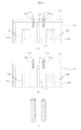
- FIG. 2 is a perspective view illustrating an RF filter according to a first embodiment of the present invention.
- the RF filter of the present invention is for example an RF cavity filter, and includes a housing member 200 , a cover 202 , an input connector 204 , an output connector 206 , cavities 208 , resonators 210 , walls 212 and tuning elements 214 .
- the housing member 200 protects elements in the RF filter, and blocks an electromagnetic wave.
- the housing member 200 may be formed by coating silver having high conductivity on an aluminum material.
- the cover 202 is combined with an upper surface of the housing member 200 , for example may be combined with the upper surface of the housing member 200 through a bolt, etc.
- the cover 202 may be formed by for example coating silver on aluminum material, and functions as a ground.
- An RF signal is inputted through the input connector 204 and is outputted through the output connector 206 .
- the RF signal propagates through coupling windows formed in each of the cavities 208 .
- Resonance of the RF signal is generated by the cavities 208 and the resonators 210 , and the RF signal is filtered by the resonance.
- the cavities 208 are defined by the walls 212 , and each of the resonators 210 is formed in corresponding cavity 208 .
- the skirt characteristic of the RF filter is enhanced but the insertion loss is deteriorated. Accordingly, the number of the resonator 210 and the cavity 208 are determined according to desired skirt characteristic and the insertion loss.
- the resonator 210 may be a cylindrical resonator as shown in FIG. 2 , but various resonators such as a disk type resonator, etc. may be employed as the resonator 210 .
- the resonator 210 may be made up of a metal or dielectric member according to mode of the RF filter, i.e. TE mode or TM mode.
- the tuning elements 214 are made up of for example a metal, are used to adjust cross coupling amount or transmission zero, and are inserted in corresponding cavity 208 under the condition that it combines with the cover 202 . It is desirable that two tuning elements 214 face on the basis of the wall 212 , i.e. a first tuning element is inserted in the cavity 208 located in the left of the wall 212 as shown in FIG. 2 and a second tuning element 214 is inserted in the cavity 208 located in the right of the wall 212 .
- the tuning elements 214 are tuning bolts, and are connected electrically each other under the condition that they combine with the cover 202 . However, the tuning elements 214 are not connected electrically to the cover 202 .
- a user may adjust cross coupling amount or transmission zero by moving up and down the tuning element 214 .
- FIG. 3 is a view illustrating schematically a part of the RF filter according to one embodiment of the present invention
- FIG. 4 is a view illustrating structure of a cover and connection structure of tuning elements according to one embodiment of the present invention.
- FIG. 5 is a view illustrating structure of a cover and connection structure of tuning elements according to another embodiment of the present invention
- FIG. 6 is a sectional view illustrating various tuning elements according to one embodiment of the present invention.
- a first resonator 210 a is disposed in a first cavity 208 a
- a second resonator 210 b is located in a second cavity 208 b
- the wall 212 is disposed between the cavities 208 a and 208 b.
- a first tuning element 214 a is inserted into the first cavity 208 a through the. cover 202 , and combines with the cover 202 through a first nut 216 a.
- a screw thread is formed on the first tuning element 214 a, and so the first tuning element 214 a moves up and down with combined with the cover 202 as shown in FIG. 3(B) in case that the first tuning element 214 a rotates.
- a groove in which a rotation tool such as a driver, etc. is inserted is formed on an upper surface of the first tuning element 214 a as shown in FIG. 3(C) .
- the user may move the first tuning element 214 a up and down by rotating the first tuning element 214 a after the user inserts the rotation tool into the groove.
- insertion depth of the first tuning element 214 a to the first cavity 208 a is changed, and thus cross coupling amount or transmission zero may be adjusted.
- a second tuning element 214 b is inserted into a second cavity 208 b through the cover 202 , faces to the first tuning element 214 a on the basis of the wall 212 , and combines with the cover 202 through a second nut 216 b.
- a screw thread is formed on the second tuning element 214 b, and so the second tuning element 214 b moves up and down with combined with the cover 202 as shown in FIG. 3(B) in case that the second tuning element 214 b rotates. As a result, cross coupling amount or transmission zero is adjusted.
- the tuning elements 214 a and 214 b are connected electrically.
- a first tuning area 402 and holes 404 a and 404 b may be formed on an upper surface 202 a of the cover 202 as shown in FIG. 4(A)
- a second tuning area 406 , a third tuning area 408 and the holes 404 a and 404 b may be formed on a rear surface of the cover 202 as shown in FIG. 4(B) .
- the first tuning element 214 a is inserted into the first cavity 208 a through the first hole 404 a
- the second tuning element 214 b is inserted into the second cavity 208 b through the second hole 404 b.
- the tuning areas 402 , 406 and 408 are conductive areas, and thus the tuning elements 214 a and 214 b are connected electrically through the first tuning area 402 formed on the upper surface 202 a of the cover 202 .
- the etching areas 400 a, 400 b and 400 c are formed. No conductive material exists in the etching areas 400 a, 400 b and 400 c.
- the tuning areas 402 , 406 and 408 are separated electrically from the conductive material of the cover 202 by the etching areas 400 a, 400 b and 400 c. Accordingly, the tuning elements 214 a and 214 b are connected electrically through the first tuning area 402 , but are not connected electrically to the coating material of the cover 202 , i.e. are not connected to the ground.
- a second tuning area, a third tuning area and holes may be formed on the upper surface 202 a of the cover 202 as shown in FIG. 5(A) , and a first tuning area and the holes may be formed on the rear surface 202 b of the cover 202 as shown in FIG. 5(B) .
- the tuning elements 214 a and 214 b are connected electrically through the first tuning area formed on the rear surface 202 b of the cover 202 .
- a tuning area and holes may be formed on the upper surface 202 a of the cover 202 as shown in FIG. 4(A) , and a tuning area and holes may be formed on the rear surface 202 b of the cover 202 as shown in FIG. 5(B) .
- the tuning elements 214 a and 214 b are connected electrically by the tuning areas.
- a groove 220 is formed on an upper surface of the wall 212 to prevent electrical connection of the conductive material in the tuning area formed on the rear surface 202 b of the cover 202 and the wall 212 .
- the user may adjust the cross coupling amount or the transmission zero in the above RF filter by changing the insertion depths of the tuning elements 214 a and 214 b to the cavities 208 a and 208 b.
- insertion depths of the tuning elements 214 a and 214 b are the same or different.
- tuning of the tuning elements 214 a and 214 b when the coupling amount is adjusted may be different from that of the tuning elements 214 a and 214 b when the transmission zero is adjusted.
- the tuning elements 21 a and 214 b may be different.
- the first tuning element 214 a may have greater thickness than the second tuning element 214 b as shown in FIG. 6(A) , or the first tuning element 214 a may have different shape and thickness compared with the second tuning element 214 b. That is, the tuning elements 214 a and 214 b may be variously modified as long as the cross coupling amount or the transmission zero is adjusted.
- FIG. 7 is a view illustrating experimental result of coupling coefficient of the RF filter according to one embodiment of the present invention
- FIG. 8 is a view illustrating experimental result of transmission zero of the RF filter according to one embodiment of the present invention.
- the coupling coefficient between the resonators 210 is changed by 0.019 (changed from 0.0191 to 0.0382).
- Coupling coefficient of the resonators in convention RF filter is changed by 0.0039.
- the RF filter of the present invention may be changed by approximately three times compared with the conventional RF filter. Accordingly, the RF filter of the present invention may tune the cross coupling amount between the resonators 210 in wide range.
- the RF filter of the present invention may adjust skirt characteristic, etc. according to spec required for the RF filter.
- FIG. 9 is a view illustrating schematically structure of an RF filter according to a second embodiment of the present invention.
- FIG. 9 does not show a housing member, resonators, etc.
- the RF filter of the present embodiment includes a cover 200 , a supporting member 900 , tuning elements 902 a and 902 b and nuts 904 a and 904 b.
- the supporting member 900 is formed on an upper surface of the cover 200 , and may be formed by coating conductive material on a dielectric member.
- a first tuning element 902 a is inserted into corresponding cavity through the supporting member 900 and the cover 200
- a second tuning element 902 b is inserted into corresponding cavity through the supporting member 900 and the cover 200 . Since an upper surface of the supporting member 900 is coated with conductive material, the tuning elements 902 a and 902 b are connected electrically. However, the tuning elements 902 a and 902 b are not connected electrically to the cover 202 because a base of the supporting member 900 is made up of dielectric member.
- the tuning elements 902 a and 902 b are fixed to the supporting member 900 by the nuts 904 a and 904 b.
- the supporting member 900 is formed on the cover 200 , and the tuning elements 902 a and 902 b are inserted into corresponding cavities through the supporting member 900 and the cover 200 . Accordingly, unlike the RF filter in the first embodiment where the upper surface of the cover is etched, the upper surface of the cover may not be etched in the RF filter of the present embodiment.
- FIG. 10 is a perspective view illustrating an RF filter according to a third embodiment of the present invention.
- the RF filter of the present invention is for example an RF cavity filter, and includes a housing member 1000 , a cover 1002 , an input connector 1004 , an output connector 1006 , cavities 1008 , resonators 1010 , walls 1012 and a third tuning element 1030 .
- the housing member 1000 , the cover 1002 , the input connector 1004 , the output connector 1006 the cavities 1008 , the resonators 1010 and the walls 1012 are the same in FIG. 2 , any further description concerning the same elements will be omitted.
- the third tuning element 1030 is for example a metal, is used for adjusting cross coupling amount or transmission zero, and is disposed on an upper surface of the cover 1002 .
- the third tuning element 1030 may be a lumped element such as a capacitor, an inductor, etc.
- FIG. 11 is a view illustrating structure of an RF filter according to a third embodiment of the present invention
- FIG. 12 is a top view illustrating a cover according to another embodiment of the present invention.
- an etching area 1200 a, a first tuning area 1202 a, a second tuning area 1202 b and a dielectric area 1210 are formed on an upper surface 1002 a of the cover 1002 .
- etching areas 1200 b and 1200 c, a third tuning area 1206 and a fourth tuning area 1208 are formed on a rear surface 1002 b of the cover 1002 .
- the tuning areas 1202 a, 1202 b, 1206 and 1208 are conductive areas, for example are coated by conductive material.
- a first hole 1204 a is formed in the first tuning area 1202 a and the third tuning area 1206
- a second hole 1204 b is formed in the second tuning area 1202 b and the fourth tuning area 1208 .
- a first tuning element 1014 a as for example a conductor is inserted into a first cavity 1008 a through the first tuning area 1202 a and the third tuning area 1206 of the cover 1002 as shown in FIG. 11 .
- a second tuning element 1014 b as for example a conductor is inserted into a second cavity 1008 b through the second tuning area 1202 b and the fourth tuning area 1208 of the cover 1002 .
- screw thread is formed on outer surfaces of the first tuning element 1014 a and the second tuning element 1014 b . Accordingly, the first tuning element 1014 a or the second tuning element 1014 b may move up and down with supported by the cover 1002 in case that the first tuning element 1014 a or the second tuning element 1014 b rotates.
- the first tuning element 1014 a is fixed to the upper surface 1002 a of the cover 1002 by a first nut 1016 a
- the second tuning element 1014 b is fixed to the upper surface 1002 a of the cover 1002 by a second nut 1016 b.
- the dielectric area 1210 locates between the first tuning area 1202 a and the second tuning area 1202 b in the first etching area 1200 a.
- the first tuning area 1200 a and the second tuning area 1200 b are separated physically; but coupling is generated between the first tuning area 1200 a and the second tuning area 1200 b by the dielectric area 1210 . That is, certain capacitance is formed between the first tuning area 1202 a and the second tuning area 1202 b.
- the first tuning element 1014 a and the second tuning element 1014 b are connected electrically through a coupling method, and so cross coupling generates between the resonators 1010 a and 1010 b in the cavities 1008 a and 1008 b where the tuning elements 1014 a and 1014 b are inserted.
- the third tuning element 1030 as a lumped element is disposed in the dielectric area 1210 .
- the capacitance between the first tuning area 1202 a and the second tuning area 1202 b is changed by the third tuning element 1030 , e.g. a capacitor, and thus cross coupling amount between the resonators 1010 a and 1010 b or transmission zero is changed.
- the cross coupling amount between the resonators 1010 a and 1010 b or the transmission zero may vary depending on the third tuning element 1030 disposed on the dielectric area 1210 as shown in FIG. 12(C) . Accordingly, the user may select properly the third tuning element 1030 to realize desired cross coupling amount or transmission.
- the user may change only the third tuning element 1030 under the condition that he fixes the first tuning element 1014 a and the second tuning element 1014 b, or change the first tuning element 1014 a or the second tuning element 1014 b as well as the third tuning element 1030 .
- the first tuning element 1014 a or the second tuning element 1014 b moves up and down.
- a groove 1020 may be formed on an upper surface of the wall 1012 to prevent electrical connection of conductive material of the tuning area 1206 and 1208 formed on the rear surface 1002 b of the cover 1002 and the wall 1012 .
- the dielectric area 1210 may be formed by removing coating material of the cover 1002 , i.e. the dielectric member of the cover 1002 is exposed.
- the RF filter of the present embodiment may adjust the cross coupling amount or the transmission zero by using the third tuning element 1030 .
- FIG. 13 is a perspective view illustrating an RF filter according to a fourth embodiment of the present invention
- FIG. 14 is a top view illustrating a cover of the RF filter in FIG. 13 according to one embodiment of the present invention.
- the RF filter of the present embodiment includes a housing. member 1000 , a cover 1002 , a first tuning element 1014 a, a second tuning element 1014 b, a first nut 1016 a, a second nut 1016 b and a tuning sliding member 1300 as a dielectric member.
- an etching area 1400 a, a first tuning area 1402 a, a second tuning area 1402 b and a dielectric area 1302 are formed on an upper surface 1002 a of the cover 1002 .
- etching areas 1400 b and 1400 c, a third tuning area 1406 and a fourth tuning area 1408 are formed on a rear surface 1002 b of the cover 1002 .
- the tuning areas 1402 a, 1402 b, 1406 and 1408 are conductive areas, for example are coated with conductive material.
- a first tuning element 1014 a is inserted into a first cavity 1008 a through the first tuning area 1402 a and the third tuning area 1406 of the cover 1002
- a second tuning element 1014 b is inserted into a second cavity 1008 b through the second tuning area 1402 b and the fourth tuning area 1408 of the cover 1002 .
- the first tuning element 1014 a is fixed to the upper surface of the cover 1002 by the first nut 1016 a
- the second tuning element 1014 b is fixed to the upper surface 1002 a of the cover 1002 by the second nut 1016 b.
- the dielectric area 1302 locates between the first tuning area 1402 a and the second tuning area 1402 b in the first etching area 1400 a.
- the first tuning area 1400 a and the second tuning area 1400 b are separated physically, but coupling generates between the first tuning area 1400 a and the second tuning area 1400 b.
- two holes 1410 and 1412 may be formed on the tuning sliding member 1300 as shown in FIG. 14(D) .
- the tuning sliding member 1300 is fixed by the first tuning element 1014 a inserted into the first cavity 1008 a through the first hole 1410 and the cover 1002 or the first nut 1016 a, and may shift left and right as shown in FIG. 14(C) under the condition that it is fixed by the first tuning element 1014 a or the first nut 1016 a.
- An end part of the tuning sliding member 1300 overlaps on the dielectric area 1302 , and capacitance between the tuning elements 1402 a and 1402 b is varied according to the overlap area. As a result, cross coupling amount between corresponding resonators or transmission zero may be changed.
- the tuning sliding member 1300 may shift front and rear direction.
- the tuning sliding member 1300 may be fixed through various methods after it is shifted to desired position.
- the RF filter of the present invention may adjust the cross coupling amount between corresponding resonators or the transmission zero by controlling the overlap area of the tuning sliding member 1300 disposed on the upper surface 1002 a of the cover 1002 and the dielectric area 1302 .
- the tuning sliding member 1300 has rectangular shape, but may have variously shapes as long as it is overlapped on the dielectric area 1302 to change the capacitance between the tuning elements 1402 a and 1402 b.
- the tuning sliding member 1300 is disposed on the position corresponding to the first tuning element 1014 a in FIG. 14 , but may be disposed on the position corresponding to the second tuning element 1014 b.
- the tuning elements 1014 a and 1014 b may move up and down through their rotation.
- FIG. 15 is a view illustrating a cover of an RF filter according to a fifth embodiment of the present invention.
- a tuning sliding member 1500 is disposed on an upper surface 1002 a of a cover 1002 in the RF filter of the present embodiment. Unlike the fourth embodiment where the tuning sliding member 1300 is supported by the first tuning element 1014 a, the tuning sliding member 1500 is disposed on the first tuning element 1014 a as shown in FIG. 15(C) .
- the tuning sliding member 1500 overlaps on a dielectric area 1502 , and so cross coupling amount between corresponding resonators or transmission zero is changed.
- a hole 1510 may be formed on the tuning sliding member 1500 as shown in FIG. 15(D) .
Landscapes
- Physics & Mathematics (AREA)
- Electromagnetism (AREA)
- Control Of Motors That Do Not Use Commutators (AREA)
Abstract
An RF filter, e.g. RF cavity filter for adjusting coupling amount or transmission zero is disclosed. The RF filter includes a housing member in which cavities are defined by walls, resonators located in the cavities, a cover combined with an upper surface of the housing member, a first tuning element inserted into a first cavity of the cavities through the cover, and a second tuning element inserted into a second cavity of the cavities through the cover. Here, the first tuning element and the second tuning element are connected electrically.
Description
- Example embodiment of the present invention relates to an RF filter, e.g. RF cavity filter for adjusting cross-coupling amount or transmission zero.
- BACKGROUND ART
- An RF cavity filter includes plural cavities, formed therein to pass only use frequency band of a signal, and is employed generally at a base station, etc. using comparative high power of a frequency signal.
-
FIG. 1 is a plan view illustration structure of a common RF cavity filter. - In
FIG. 1 , the RF cavity filter includes aninput connector 100, anoutput connector 102, ahousing member 104,cavities housing member 104 and a wall,resonators cavities coupling bar 160. - An RF signal inputted through the
input connector 100 is provided to thecavity 110. Each of thecavities corresponding resonators - The RF signal is delivered from one cavity to another cavity through a
coupling window 150. - A resonance frequency of the filter is determined by size of the cavities and size of the resonators. A user may tune finely characteristics of the filter using tuning bolts which are not shown.
- The skirt characteristic which means a slope of a boundary band in a pass band characteristic curve is important in view of the filter, and preferably should be formed sharply.
- The skirt characteristic is improved according as order of the filter increases, i.e. the number of the cavities and the resonators increases. However, the skirt characteristic has trade-off relation with an insertion loss. That is, as the number of the cavities and the resonators increases, the skirt characteristic is enhanced but the insertion loss augments.
- The filter forms a notch using cross coupling to improve the skirt characteristic with maintaining constant insertion loss.
- The cross coupling means coupling between resonators which are not adjacent, e.g. coupling between a
second resonator 132 and afifth resonator 138. The cross coupling is realized generally through thecoupling bar 160. - The
coupling bar 160 is formed through a wall between the second cavity 122 and the fifth cavity 128, and is made up of a metal. Thecoupling bar 160 functions to deliver for example a signal of thesecond resonator 132 to thefifth resonator 138. - A hole for the
coupling bar 160 is formed on the wall between the second cavity 122 and the fifth cavity 128, a dielectric layer is formed on an inner surface of the wall corresponding to the hole, and so thecoupling bar 160 is not connected electrically to the wall. - However, this cross coupling structure may not adjust coupling amount between resonators. The coupling amount is determined by size of the
coupling bar 160, and thus thecoupling bar 160 should be replaced by new coupling bar having different size in case that desired coupling amount is not realized. In addition, the coupling amount may not be adjusted under the condition that thecoupling bar 160 is set on the wall. - Moreover, the filter may not adjust transmission zero related to the skirt characteristic.
- Example embodiment of the present invention provides an RF filter, for example RF cavity filter for adjusting cross coupling amount or transmission zero.
- An RF filter according to one embodiment of the present invention includes a housing member in which cavities are defined by walls; resonators located in the cavities; a cover combined with an upper surface of the housing member; a first tuning element inserted into a first cavity of the cavities through the cover; and a second tuning element inserted into a second cavity of the cavities through the cover. Here, the first tuning element and the second tuning element are connected electrically.
- An RF filter according to another embodiment of the present invention includes a housing member; a cover combined with an upper surface of the housing member; a first tuning area formed on one surface of the cover; a second tuning area formed on the one surface of the cover with separated from the first tuning area; a dielectric area formed between the first tuning area and the second tuning area on the one surface of the cover; and a third tuning element disposed on the dielectric area. Here, the first tuning area and the second tuning area are conductive areas.
- An RF filter according to still another embodiment of the present invention includes a housing member; a cover combined with an upper surface of the housing member; a first tuning area formed on one surface of the cover; a second tuning area formed on the one surface of the cover with separated from the first tuning area; a dielectric area formed between the first tuning area and the second tuning area on the one surface of the cover; a first tuning element inserted into the housing member through the first tuning area of the cover; a second tuning element inserted into the housing member through the second tuning element of the cover; and a tuning sliding member disposed on the one surface of the cover. Here, a part of the tuning sliding member overlaps with the dielectric area.
- An RF filter according to the present invention controls tuning elements inserted in corresponding cavities through a cover, thereby adjusting cross coupling amount or transmission zero. Specially, variable range of coupling coefficient and transmission zero may be considerably wide.
- The RF filter according to the present invention adjusts capacitance between the tuning elements using a lumped element or a tuning sliding member under the condition that the tuning elements are inserted into corresponding cavities through the cover, and so cross coupling amount between corresponding resonators or transmission zero may be adjusted. Specially, a user may control the lumped element and the tuning sliding member outside to tune easily characteristics of the filter.
- Example embodiments of the present invention will become more apparent by describing in detail example embodiments of the present invention with reference to the accompanying drawings, in which:
-
FIG. 1 is a plan view illustration structure of a common RF cavity filter; -
FIG. 2 is a perspective view illustrating an RF filter according to a first embodiment of the present invention; -
FIG. 3 is a view illustrating schematically a part of the RF filter according to one embodiment of the present invention; -
FIG. 4 is a view illustrating structure of a cover and connection structure of tuning elements according to one embodiment of the present invention; -
FIG. 5 is a view illustrating structure of a cover and connection structure of tuning elements according to another embodiment of the present invention; -
FIG. 6 is a sectional view illustrating various tuning elements according to one embodiment of the present invention; -
FIG. 7 is a view illustrating experimental result of coupling coefficient of the RF filter according to one embodiment of the present invention; -
FIG. 8 is a view illustrating experimental result of transmission zero of the RF filter according to one embodiment of the present invention; -
FIG. 9 is a view illustrating schematically structure of an RF filter according to a second embodiment of the present invention; -
FIG. 10 is a perspective view illustrating an RF filter according to a third embodiment of the present invention; -
FIG. 11 is a view illustrating structure of an RF filter according to a third embodiment of the present invention; -
FIG. 12 is a top view illustrating a cover according to another embodiment of the present invention; -
FIG. 13 is a perspective view illustrating an RF filter according to a fourth embodiment of the present invention; -
FIG. 14 is a top view illustrating a cover of the RF filter inFIG. 13 according to one embodiment of the present invention; and -
FIG. 15 is a view illustrating a cover of an RF filter according to a fifth embodiment of the present invention. - Hereinafter, embodiments of the present invention will be described in detail with reference to accompanying drawings.
-
FIG. 2 is a perspective view illustrating an RF filter according to a first embodiment of the present invention. - In
FIG. 2 , the RF filter of the present invention is for example an RF cavity filter, and includes ahousing member 200, acover 202, aninput connector 204, anoutput connector 206,cavities 208,resonators 210,walls 212 andtuning elements 214. - The
housing member 200 protects elements in the RF filter, and blocks an electromagnetic wave. Thehousing member 200 may be formed by coating silver having high conductivity on an aluminum material. - The
cover 202 is combined with an upper surface of thehousing member 200, for example may be combined with the upper surface of thehousing member 200 through a bolt, etc. Thecover 202 may be formed by for example coating silver on aluminum material, and functions as a ground. - An RF signal is inputted through the
input connector 204 and is outputted through theoutput connector 206. Here, the RF signal propagates through coupling windows formed in each of thecavities 208. Resonance of the RF signal is generated by thecavities 208 and theresonators 210, and the RF signal is filtered by the resonance. - The
cavities 208 are defined by thewalls 212, and each of theresonators 210 is formed in correspondingcavity 208. As the number of theresonator 210 and thecavity 208 increases, the skirt characteristic of the RF filter is enhanced but the insertion loss is deteriorated. Accordingly, the number of theresonator 210 and thecavity 208 are determined according to desired skirt characteristic and the insertion loss. - The
resonator 210 may be a cylindrical resonator as shown inFIG. 2 , but various resonators such as a disk type resonator, etc. may be employed as theresonator 210. Theresonator 210 may be made up of a metal or dielectric member according to mode of the RF filter, i.e. TE mode or TM mode. - The tuning
elements 214 are made up of for example a metal, are used to adjust cross coupling amount or transmission zero, and are inserted in correspondingcavity 208 under the condition that it combines with thecover 202. It is desirable that two tuningelements 214 face on the basis of thewall 212, i.e. a first tuning element is inserted in thecavity 208 located in the left of thewall 212 as shown inFIG. 2 and asecond tuning element 214 is inserted in thecavity 208 located in the right of thewall 212. - In one embodiment of the present invention, the tuning
elements 214 are tuning bolts, and are connected electrically each other under the condition that they combine with thecover 202. However, the tuningelements 214 are not connected electrically to thecover 202. - A user may adjust cross coupling amount or transmission zero by moving up and down the
tuning element 214. - Hereinafter, a process of adjusting coupling amount or transmission zero using the
tuning elements 214 and disposition of the tuningelements 214 will be described in detail with reference to accompanying drawings. -
FIG. 3 is a view illustrating schematically a part of the RF filter according to one embodiment of the present invention, andFIG. 4 is a view illustrating structure of a cover and connection structure of tuning elements according to one embodiment of the present invention.FIG. 5 is a view illustrating structure of a cover and connection structure of tuning elements according to another embodiment of the present invention, andFIG. 6 is a sectional view illustrating various tuning elements according to one embodiment of the present invention. - In
FIG. 3(A) , afirst resonator 210 a is disposed in a first cavity 208 a, a second resonator 210 b is located in a second cavity 208 b, and thewall 212 is disposed between the cavities 208 a and 208 b. - A
first tuning element 214 a is inserted into the first cavity 208 a through the. cover 202, and combines with thecover 202 through afirst nut 216 a. A screw thread is formed on thefirst tuning element 214 a, and so thefirst tuning element 214 a moves up and down with combined with thecover 202 as shown inFIG. 3(B) in case that thefirst tuning element 214 a rotates. It is desirable that a groove in which a rotation tool such as a driver, etc. is inserted is formed on an upper surface of thefirst tuning element 214 a as shown inFIG. 3(C) . The user may move thefirst tuning element 214 a up and down by rotating thefirst tuning element 214 a after the user inserts the rotation tool into the groove. As a result, insertion depth of thefirst tuning element 214 a to the first cavity 208 a is changed, and thus cross coupling amount or transmission zero may be adjusted. - A
second tuning element 214 b is inserted into a second cavity 208 b through thecover 202, faces to thefirst tuning element 214 a on the basis of thewall 212, and combines with thecover 202 through a second nut 216 b. A screw thread is formed on thesecond tuning element 214 b, and so thesecond tuning element 214 b moves up and down with combined with thecover 202 as shown inFIG. 3(B) in case that thesecond tuning element 214 b rotates. As a result, cross coupling amount or transmission zero is adjusted. - The tuning
elements first tuning area 402 andholes upper surface 202 a of thecover 202 as shown inFIG. 4(A) , and asecond tuning area 406, athird tuning area 408 and theholes cover 202 as shown inFIG. 4(B) . Thefirst tuning element 214 a is inserted into the first cavity 208 a through thefirst hole 404 a, and thesecond tuning element 214 b is inserted into the second cavity 208 b through thesecond hole 404 b. Here, the tuningareas tuning elements first tuning area 402 formed on theupper surface 202 a of thecover 202. - In case of etching the upper surface and the rear surface of the
cover 202 formed by coating conductive material on a dielectric member according to thetuning areas etching areas etching areas areas cover 202 by theetching areas elements first tuning area 402, but are not connected electrically to the coating material of thecover 202, i.e. are not connected to the ground. - In another embodiment of the present invention, a second tuning area, a third tuning area and holes may be formed on the
upper surface 202 a of thecover 202 as shown inFIG. 5(A) , and a first tuning area and the holes may be formed on therear surface 202 b of thecover 202 as shown inFIG. 5(B) . The tuningelements rear surface 202 b of thecover 202. - In still another embodiment of the present invention, a tuning area and holes may be formed on the
upper surface 202 a of thecover 202 as shown inFIG. 4(A) , and a tuning area and holes may be formed on therear surface 202 b of thecover 202 as shown inFIG. 5(B) . The tuningelements - In still another embodiment of the present invention, a
groove 220 is formed on an upper surface of thewall 212 to prevent electrical connection of the conductive material in the tuning area formed on therear surface 202 b of thecover 202 and thewall 212. - The user may adjust the cross coupling amount or the transmission zero in the above RF filter by changing the insertion depths of the tuning
elements elements elements elements - On the other hand, length, thickness and shape, etc. of the
tuning elements 21 a and 214 b may be different. For example, thefirst tuning element 214 a may have greater thickness than thesecond tuning element 214 b as shown inFIG. 6(A) , or thefirst tuning element 214 a may have different shape and thickness compared with thesecond tuning element 214 b. That is, the tuningelements - Hereinafter, experimental result of coupling characteristics of the RF filter according to the present invention will be described in detail.
-
FIG. 7 is a view illustrating experimental result of coupling coefficient of the RF filter according to one embodiment of the present invention, andFIG. 8 is a view illustrating experimental result of transmission zero of the RF filter according to one embodiment of the present invention. - Referring to
FIG. 7 , it is verified that the coupling coefficient between theresonators 210 is changed by 0.019 (changed from 0.0191 to 0.0382). Coupling coefficient of the resonators in convention RF filter is changed by 0.0039. In other words, the RF filter of the present invention may be changed by approximately three times compared with the conventional RF filter. Accordingly, the RF filter of the present invention may tune the cross coupling amount between theresonators 210 in wide range. - In
FIG. 8 , it is verified that the transmission zero is changed from 1.805 GHz to 1.907 GHz. That is, the transmission zero is changed by 102 MHz. However, the transmission zero may be changed by above 102 MHz. Accordingly, the RF filter of the present invention may adjust skirt characteristic, etc. according to spec required for the RF filter. -
FIG. 9 is a view illustrating schematically structure of an RF filter according to a second embodiment of the present invention.FIG. 9 does not show a housing member, resonators, etc. - In
FIG. 9 , the RF filter of the present embodiment includes acover 200, a supportingmember 900, tuningelements nuts 904 a and 904 b. - The supporting
member 900 is formed on an upper surface of thecover 200, and may be formed by coating conductive material on a dielectric member. - A
first tuning element 902 a is inserted into corresponding cavity through the supportingmember 900 and thecover 200, and asecond tuning element 902 b is inserted into corresponding cavity through the supportingmember 900 and thecover 200. Since an upper surface of the supportingmember 900 is coated with conductive material, the tuningelements elements cover 202 because a base of the supportingmember 900 is made up of dielectric member. - The tuning
elements member 900 by thenuts 904 a and 904 b. - In brief, in the RF filter, the supporting
member 900 is formed on thecover 200, and thetuning elements member 900 and thecover 200. Accordingly, unlike the RF filter in the first embodiment where the upper surface of the cover is etched, the upper surface of the cover may not be etched in the RF filter of the present embodiment. -
FIG. 10 is a perspective view illustrating an RF filter according to a third embodiment of the present invention. - In
FIG. 10 , the RF filter of the present invention is for example an RF cavity filter, and includes ahousing member 1000, acover 1002, aninput connector 1004, anoutput connector 1006,cavities 1008,resonators 1010,walls 1012 and athird tuning element 1030. - Since the
housing member 1000, thecover 1002, theinput connector 1004, theoutput connector 1006 thecavities 1008, theresonators 1010 and thewalls 1012 are the same inFIG. 2 , any further description concerning the same elements will be omitted. - The
third tuning element 1030 is for example a metal, is used for adjusting cross coupling amount or transmission zero, and is disposed on an upper surface of thecover 1002. - In one embodiment of the present invention, the
third tuning element 1030 may be a lumped element such as a capacitor, an inductor, etc. - Hereinafter, a process of adjusting coupling amount or transmission zero using the
third tuning element 1030 and structure of the RF filter will be described in detail with reference to accompanying drawings. -
FIG. 11 is a view illustrating structure of an RF filter according to a third embodiment of the present invention, andFIG. 12 is a top view illustrating a cover according to another embodiment of the present invention. - In
FIG. 12(A) , anetching area 1200 a, afirst tuning area 1202 a, asecond tuning area 1202 b and adielectric area 1210 are formed on anupper surface 1002 a of thecover 1002. - In
FIG. 12(B) ,etching areas fourth tuning area 1208 are formed on arear surface 1002 b of thecover 1002. - The
tuning areas - A
first hole 1204 a is formed in thefirst tuning area 1202 a and the third tuning area 1206, and asecond hole 1204 b is formed in thesecond tuning area 1202 b and thefourth tuning area 1208. Afirst tuning element 1014 a as for example a conductor is inserted into a first cavity 1008 a through thefirst tuning area 1202 a and the third tuning area 1206 of thecover 1002 as shown inFIG. 11 . Asecond tuning element 1014 b as for example a conductor is inserted into asecond cavity 1008 b through thesecond tuning area 1202 b and thefourth tuning area 1208 of thecover 1002. - In one embodiment of the present invention, screw thread is formed on outer surfaces of the
first tuning element 1014 a and thesecond tuning element 1014 b. Accordingly, thefirst tuning element 1014 a or thesecond tuning element 1014 b may move up and down with supported by thecover 1002 in case that thefirst tuning element 1014 a or thesecond tuning element 1014 b rotates. - The
first tuning element 1014 a is fixed to theupper surface 1002 a of thecover 1002 by afirst nut 1016 a, and thesecond tuning element 1014 b is fixed to theupper surface 1002 a of thecover 1002 by asecond nut 1016 b. - The
dielectric area 1210 locates between thefirst tuning area 1202 a and thesecond tuning area 1202 b in thefirst etching area 1200 a. Here, thefirst tuning area 1200 a and thesecond tuning area 1200 b are separated physically; but coupling is generated between thefirst tuning area 1200 a and thesecond tuning area 1200 b by thedielectric area 1210. That is, certain capacitance is formed between thefirst tuning area 1202 a and thesecond tuning area 1202 b. Accordingly, thefirst tuning element 1014 a and thesecond tuning element 1014 b are connected electrically through a coupling method, and so cross coupling generates between theresonators 1010 a and 1010 b in thecavities 1008 a and 1008 b where thetuning elements - In one embodiment of the present invention, the
third tuning element 1030 as a lumped element is disposed in thedielectric area 1210. As a result, the capacitance between thefirst tuning area 1202 a and thesecond tuning area 1202 b is changed by thethird tuning element 1030, e.g. a capacitor, and thus cross coupling amount between theresonators 1010 a and 1010 b or transmission zero is changed. In other words, the cross coupling amount between theresonators 1010 a and 1010 b or the transmission zero may vary depending on thethird tuning element 1030 disposed on thedielectric area 1210 as shown inFIG. 12(C) . Accordingly, the user may select properly thethird tuning element 1030 to realize desired cross coupling amount or transmission. - In one embodiment of the present invention, to adjust the cross coupling amount or the transmission zero, the user may change only the
third tuning element 1030 under the condition that he fixes thefirst tuning element 1014 a and thesecond tuning element 1014 b, or change thefirst tuning element 1014 a or thesecond tuning element 1014 b as well as thethird tuning element 1030. Here, thefirst tuning element 1014 a or thesecond tuning element 1014 b moves up and down. - In another embodiment of the present invention, a
groove 1020 may be formed on an upper surface of thewall 1012 to prevent electrical connection of conductive material of thetuning area 1206 and 1208 formed on therear surface 1002 b of thecover 1002 and thewall 1012. - The
dielectric area 1210 may be formed by removing coating material of thecover 1002, i.e. the dielectric member of thecover 1002 is exposed. - In short, the RF filter of the present embodiment may adjust the cross coupling amount or the transmission zero by using the
third tuning element 1030. -
FIG. 13 is a perspective view illustrating an RF filter according to a fourth embodiment of the present invention, andFIG. 14 is a top view illustrating a cover of the RF filter inFIG. 13 according to one embodiment of the present invention. - In
FIG. 13 , the RF filter of the present embodiment includes a housing.member 1000, acover 1002, afirst tuning element 1014 a, asecond tuning element 1014 b, afirst nut 1016 a, asecond nut 1016 b and atuning sliding member 1300 as a dielectric member. - In
FIG. 14 , anetching area 1400 a, afirst tuning area 1402 a, asecond tuning area 1402 b and adielectric area 1302 are formed on anupper surface 1002 a of thecover 1002. - In
FIG. 14(B) ,etching areas third tuning area 1406 and afourth tuning area 1408 are formed on arear surface 1002 b of thecover 1002. - The
tuning areas - A
first tuning element 1014 a is inserted into a first cavity 1008 a through thefirst tuning area 1402 a and thethird tuning area 1406 of thecover 1002, and asecond tuning element 1014 b is inserted into asecond cavity 1008 b through thesecond tuning area 1402 b and thefourth tuning area 1408 of thecover 1002. - The
first tuning element 1014 a is fixed to the upper surface of thecover 1002 by thefirst nut 1016 a, and thesecond tuning element 1014 b is fixed to theupper surface 1002 a of thecover 1002 by thesecond nut 1016 b. - The
dielectric area 1302 locates between thefirst tuning area 1402 a and thesecond tuning area 1402 b in thefirst etching area 1400 a. Thefirst tuning area 1400 a and thesecond tuning area 1400 b are separated physically, but coupling generates between thefirst tuning area 1400 a and thesecond tuning area 1400 b. - In one embodiment of the present invention, two
holes tuning sliding member 1300 as shown inFIG. 14(D) . Thetuning sliding member 1300 is fixed by thefirst tuning element 1014 a inserted into the first cavity 1008 a through thefirst hole 1410 and thecover 1002 or thefirst nut 1016 a, and may shift left and right as shown inFIG. 14(C) under the condition that it is fixed by thefirst tuning element 1014 a or thefirst nut 1016 a. An end part of thetuning sliding member 1300 overlaps on thedielectric area 1302, and capacitance between the tuningelements tuning sliding member 1300 may shift front and rear direction. Thetuning sliding member 1300 may be fixed through various methods after it is shifted to desired position. - In brief, the RF filter of the present invention may adjust the cross coupling amount between corresponding resonators or the transmission zero by controlling the overlap area of the
tuning sliding member 1300 disposed on theupper surface 1002 a of thecover 1002 and thedielectric area 1302. - In above description, the
tuning sliding member 1300 has rectangular shape, but may have variously shapes as long as it is overlapped on thedielectric area 1302 to change the capacitance between the tuningelements - The
tuning sliding member 1300 is disposed on the position corresponding to thefirst tuning element 1014 a inFIG. 14 , but may be disposed on the position corresponding to thesecond tuning element 1014 b. - The
tuning elements -
FIG. 15 is a view illustrating a cover of an RF filter according to a fifth embodiment of the present invention. - In
FIG. 15 , atuning sliding member 1500 is disposed on anupper surface 1002 a of acover 1002 in the RF filter of the present embodiment. Unlike the fourth embodiment where thetuning sliding member 1300 is supported by thefirst tuning element 1014 a, thetuning sliding member 1500 is disposed on thefirst tuning element 1014 a as shown inFIG. 15(C) . Thetuning sliding member 1500 overlaps on adielectric area 1502, and so cross coupling amount between corresponding resonators or transmission zero is changed. - A
hole 1510 may be formed on thetuning sliding member 1500 as shown inFIG. 15(D) . - Although embodiments have been described with reference to a number of illustrative embodiments thereof, it should be understood that numerous other modifications and embodiments can be devised by those skilled in the art that will fall within the spirit and scope of the principles of this disclosure. More particularly, various variations and modifications are possible in the component parts and/or arrangements of the subject combination arrangement within the scope of the disclosure, the drawings and the appended claims. In addition to variations and modifications in the component parts and/or arrangements, alternative uses will also be apparent to those skilled in the art.
Claims (15)
1. An RF filter comprising:
a housing member in which cavities are defined by walls;
resonators located in the cavities;
a cover combined with an upper surface of the housing member;
a first tuning element inserted into a first cavity of the cavities through the cover; and
a second tuning element inserted into a second cavity of the cavities through the cover,
wherein the first tuning element and the second tuning element are connected electrically.
2. The RF filter of claim 1 , wherein the cover is formed by coating conductive material on a dielectric member, a first tuning area is formed by etching a part of one surface of the cover, a second tuning area and a third tuning area are formed by etching a part of other surface facing to the one surface of the cover,
the first tuning element is inserted into the first cavity through the first tuning area and the second tuning area, the second tuning element is inserted into the second cavity through the first tuning area and the third tuning area, the first tuning element and the second tuning element are connected electrically by conductive material in the first tuning area.
3. The RF filter of claim 2 , wherein the first tuning clement and the second tuning element move up and down of the cover, and coupling amount between a first resonator inserted into the first cavity and a second resonator inserted into the second cavity or transmission zero is adjusted according to movement of the first tuning element and the second tuning element.
4. The RF filter of claim 1 , further comprising:
the wall configured to separate the first cavity from the second cavity,
wherein the cover is formed by coating conductive material on a dielectric member, a tuning area is formed by etching a part of a rear surface of the cover, a groove is formed on an upper surface of the wall, and the tuning area corresponds to the groove.
5. The RF filter of claim 1 , wherein the first tuning element is fixed to an upper surface of the cover by a first nut, and the second tuning element is fixed to the upper surface of the cover by a second nut.
6. The RF filter of claim 1 , wherein thickness or length of the first tuning element is different from that of the second tuning element.
7. The RF filter of claim 1 , further comprising:
a supporting member formed on an upper surface of the cover,
wherein the first tuning element is inserted into the first cavity through the supporting member and the cover, the second tuning element is inserted into the second cavity through the supporting member and the cover, the supporting member is formed by coating conductive material on a dielectric member, and the first tuning element and the second tuning element are connected electrically through the conductive material of the supporting member.
8. An RF filter comprising:
a housing member;
a cover combined with an upper surface of the housing member;
a first tuning area formed on one surface of the cover;
a second tuning area formed on the one surface of the cover with separated from the first tuning area;
a dielectric area formed between the first tuning area and the second tuning area on the one surface of the cover; and
a third tuning element disposed on the dielectric area,
wherein the first tuning area and the second tuning area are conductive areas.
9. The RF filter of claim 8 , further comprising:
cavities defined by walls in the housing member;
resonators located in the cavities;
a third tuning area formed on other surface facing to the one surface of the cover;
a fourth tuning area formed on the other surface of the cover with separated from the third tuning area;
a first tuning element inserted into a first cavity of the cavities through the first tuning area and the third tuning area of the cover; and
a second tuning element inserted into a second cavity of the cavities through the second tuning element and the fourth tuning element of the cover,
wherein the cover is formed by coating conductive material on a dielectric member, the third tuning element is an lumped element, the first tuning area and the second tuning area are formed by etching a part of the one surface of the cover, the third tuning area and the fourth tuning area are formed by etching a part of the other surface of the cover, cross coupling amount between corresponding resonators or transmission zero depends on the third tuning element.
10. The RF filter of claim 9 , wherein each of the first tuning element and the second tuning element is a bolt, the first tuning element is fixed to an upper surface of the cover by a first nut, and the second tuning element is fixed to the upper surface of the cover by a second nut,
the first tuning element and the second tuning element are disposed symmetrically on the basis of specific wall, a groove is formed on an upper surface of the wall, and the first tuning element and the second tuning element move up and down.
11. An RF filter comprising:
a housing member;
a cover combined with an upper surface of the housing member;
a first tuning area formed on one surface of the cover;
a second tuning area formed on the one surface of the cover with separated from the first tuning area;
a dielectric area formed between the first tuning area and the second tuning area on the one surface of the cover;
a first tuning element inserted into the housing member through the first tuning area of the cover;
a second tuning element inserted into the housing member through the second tuning element of the cover; and
a tuning sliding member disposed on the one surface of the cover,
wherein a part of the tuning sliding member overlaps with the dielectric area.
12. The RF filter of claim II, further comprising:
cavities defined by walls in the housing member; and
resonators located in the cavities,
wherein a first hole and a second hole are formed on a part of the tuning sliding member, the tuning sliding member slides with supported by the first tuning element through the first hole, and cross coupling amount between corresponding resonators or transmission zero are varied depending on an overlap area of the tuning sliding member and the dielectric area.
13. The RF filter of claim 11 , further comprising:
cavities defined by walls in the housing member; and
resonators located in the cavities,
wherein the tuning sliding member slides with disposed on the first tuning element, and cross coupling amount between corresponding resonators or transmission zero are varied depending on an overlap area of the tuning sliding member and the dielectric area.
14. The RF filter of claim 11 , wherein the cover is formed by coating conductive material on a dielectric member, the first tuning area and the second tuning area are formed by etching a part of the one surface of the cover, and the tuning sliding member is made up of dielectric material.
15. The RF filter of claim 11 , wherein at least one of the first tuning element and the second tuning element moves up and down, each of the first tuning element and the second tuning element is a bolt, the first tuning element is fixed to the one surface of the cover by a first nut, and the second tuning element is fixed to the one surface of the cover by a second nut,
the first tuning element and the second tuning element are disposed symmetrically on the basis of specific wall, and a groove is formed on an upper surface of the wall.
Priority Applications (1)
| Application Number | Priority Date | Filing Date | Title |
|---|---|---|---|
| US14/709,354 US9887442B2 (en) | 2011-03-31 | 2015-05-11 | RF filter for adjusting coupling amount or transmission zero |
Applications Claiming Priority (4)
| Application Number | Priority Date | Filing Date | Title |
|---|---|---|---|
| KR10-2011-0029883 | 2011-03-31 | ||
| KR1020110029883A KR101216910B1 (en) | 2011-03-31 | 2011-03-31 | Rf filter for tuning coupling amount or transmission zero |
| KR1020110029866A KR101207141B1 (en) | 2011-03-31 | 2011-03-31 | Rf filter for tuning coupling amount or transmission zero |
| KR10-2011-0029866 | 2011-03-31 |
Related Child Applications (1)
| Application Number | Title | Priority Date | Filing Date |
|---|---|---|---|
| US14/709,354 Division US9887442B2 (en) | 2011-03-31 | 2015-05-11 | RF filter for adjusting coupling amount or transmission zero |
Publications (1)
| Publication Number | Publication Date |
|---|---|
| US20120249266A1 true US20120249266A1 (en) | 2012-10-04 |
Family
ID=46926437
Family Applications (2)
| Application Number | Title | Priority Date | Filing Date |
|---|---|---|---|
| US13/434,679 Abandoned US20120249266A1 (en) | 2011-03-31 | 2012-03-29 | Rf filter for adjusting coupling amount or transmission zero |
| US14/709,354 Active 2032-05-18 US9887442B2 (en) | 2011-03-31 | 2015-05-11 | RF filter for adjusting coupling amount or transmission zero |
Family Applications After (1)
| Application Number | Title | Priority Date | Filing Date |
|---|---|---|---|
| US14/709,354 Active 2032-05-18 US9887442B2 (en) | 2011-03-31 | 2015-05-11 | RF filter for adjusting coupling amount or transmission zero |
Country Status (1)
| Country | Link |
|---|---|
| US (2) | US20120249266A1 (en) |
Cited By (32)
| Publication number | Priority date | Publication date | Assignee | Title |
|---|---|---|---|---|
| CN103985933A (en) * | 2013-01-28 | 2014-08-13 | Ace技术株式会社 | Multi-vibration-mode filter capable of adjusting transmission zero |
| EP2814112A1 (en) * | 2013-06-13 | 2014-12-17 | Alcatel Lucent | Resonant assembly |
| EP2814111A1 (en) * | 2013-06-13 | 2014-12-17 | Alcatel Lucent | Resonant assembly |
| US20150092625A1 (en) * | 2013-03-15 | 2015-04-02 | Rf Micro Devices, Inc. | Hybrid active and passive tunable rf filters |
| US9419578B2 (en) | 2013-06-06 | 2016-08-16 | Qorvo Us, Inc. | Tunable RF filter paths for tunable RF filter structures |
| US9444417B2 (en) | 2013-03-15 | 2016-09-13 | Qorvo Us, Inc. | Weakly coupled RF network based power amplifier architecture |
| US9444411B2 (en) | 2013-03-15 | 2016-09-13 | Qorvo Us, Inc. | RF power amplifier with total radiated power stabilization |
| US9628045B2 (en) | 2013-08-01 | 2017-04-18 | Qorvo Us, Inc. | Cooperative tunable RF filters |
| US9685928B2 (en) | 2013-08-01 | 2017-06-20 | Qorvo Us, Inc. | Interference rejection RF filters |
| US9705478B2 (en) | 2013-08-01 | 2017-07-11 | Qorvo Us, Inc. | Weakly coupled tunable RF receiver architecture |
| US9705542B2 (en) | 2013-06-06 | 2017-07-11 | Qorvo Us, Inc. | Reconfigurable RF filter |
| US9755671B2 (en) | 2013-08-01 | 2017-09-05 | Qorvo Us, Inc. | VSWR detector for a tunable filter structure |
| US9774311B2 (en) | 2013-03-15 | 2017-09-26 | Qorvo Us, Inc. | Filtering characteristic adjustments of weakly coupled tunable RF filters |
| US9780756B2 (en) | 2013-08-01 | 2017-10-03 | Qorvo Us, Inc. | Calibration for a tunable RF filter structure |
| US9780817B2 (en) | 2013-06-06 | 2017-10-03 | Qorvo Us, Inc. | RX shunt switching element-based RF front-end circuit |
| US9800282B2 (en) | 2013-06-06 | 2017-10-24 | Qorvo Us, Inc. | Passive voltage-gain network |
| US9825656B2 (en) | 2013-08-01 | 2017-11-21 | Qorvo Us, Inc. | Weakly coupled tunable RF transmitter architecture |
| US9859863B2 (en) | 2013-03-15 | 2018-01-02 | Qorvo Us, Inc. | RF filter structure for antenna diversity and beam forming |
| US9871499B2 (en) | 2013-03-15 | 2018-01-16 | Qorvo Us, Inc. | Multi-band impedance tuners using weakly-coupled LC resonators |
| US9899133B2 (en) | 2013-08-01 | 2018-02-20 | Qorvo Us, Inc. | Advanced 3D inductor structures with confined magnetic field |
| US9966981B2 (en) | 2013-06-06 | 2018-05-08 | Qorvo Us, Inc. | Passive acoustic resonator based RF receiver |
| CN110416681A (en) * | 2019-08-01 | 2019-11-05 | 电子科技大学 | Device and method for wide-band adaptive adjustment of resonance cavity coupling amount |
| WO2019240486A1 (en) * | 2018-06-12 | 2019-12-19 | 주식회사 케이엠더블유 | Cavity filter and connecting structure included therein |
| US10796835B2 (en) | 2015-08-24 | 2020-10-06 | Qorvo Us, Inc. | Stacked laminate inductors for high module volume utilization and performance-cost-size-processing-time tradeoff |
| CN112787055A (en) * | 2019-11-07 | 2021-05-11 | 深圳市大富科技股份有限公司 | Cavity filter and communication radio frequency device |
| CN113036371A (en) * | 2019-12-25 | 2021-06-25 | 深圳市大富科技股份有限公司 | Filter and communication equipment |
| US11139238B2 (en) | 2016-12-07 | 2021-10-05 | Qorvo Us, Inc. | High Q factor inductor structure |
| CN113922024A (en) * | 2020-07-09 | 2022-01-11 | 大富科技(安徽)股份有限公司 | Filter and communication equipment |
| WO2022218113A1 (en) * | 2021-04-16 | 2022-10-20 | 京信射频技术(广州)有限公司 | Metal filter, filtering loop module, and method for adjusting amount of coupling |
| US11646760B2 (en) | 2019-09-23 | 2023-05-09 | Ticona Llc | RF filter for use at 5G frequencies |
| US11876273B2 (en) | 2018-06-12 | 2024-01-16 | Kmw Inc. | Terminal portion configured to connect an RF signal connector to an electrode pad of an external device over a predetermined distance |
| US12224096B2 (en) | 2013-03-15 | 2025-02-11 | Qorvo Us, Inc. | Advanced 3D inductor structures with confined magnetic field |
Families Citing this family (3)
| Publication number | Priority date | Publication date | Assignee | Title |
|---|---|---|---|---|
| WO2018137315A1 (en) * | 2017-01-26 | 2018-08-02 | 深圳市国人射频通信有限公司 | Tunable capacitive cross-coupling structure and cavity filter |
| IT202100012983A1 (en) * | 2021-05-19 | 2022-11-19 | Commscope Italy Srl | FIXING ELEMENT FOR THE RESONATOR OF A RADIOFREQUENCY FILTER |
| KR102701941B1 (en) * | 2022-10-13 | 2024-09-04 | 주식회사 넥스웨이브 | Cavity filter for radio frequency wireless communication |
Citations (4)
| Publication number | Priority date | Publication date | Assignee | Title |
|---|---|---|---|---|
| US4100504A (en) * | 1977-06-20 | 1978-07-11 | Harris Corporation | Band rejection filter having integrated impedance inverter-tune cavity configuration |
| US6366184B1 (en) * | 1999-03-03 | 2002-04-02 | Filtronic Lk Oy | Resonator filter |
| US20020145490A1 (en) * | 2001-04-04 | 2002-10-10 | Adc Telecommunications, Inc. | Filter structure including circuit board |
| US6781476B2 (en) * | 2002-01-08 | 2004-08-24 | Murata Manufacturing Co., Ltd. | Filter having directional coupler and communication device |
Family Cites Families (4)
| Publication number | Priority date | Publication date | Assignee | Title |
|---|---|---|---|---|
| US6255917B1 (en) * | 1999-01-12 | 2001-07-03 | Teledyne Technologies Incorporated | Filter with stepped impedance resonators and method of making the filter |
| US6559740B1 (en) * | 2001-12-18 | 2003-05-06 | Delta Microwave, Inc. | Tunable, cross-coupled, bandpass filter |
| EP2031693B1 (en) * | 2007-08-28 | 2014-04-30 | ACE Technology | Frequency tunable filter |
| KR101045498B1 (en) * | 2008-08-07 | 2011-06-30 | 주식회사 에이스테크놀로지 | Tunable filter with adjustable tuning characteristics |
-
2012
- 2012-03-29 US US13/434,679 patent/US20120249266A1/en not_active Abandoned
-
2015
- 2015-05-11 US US14/709,354 patent/US9887442B2/en active Active
Patent Citations (4)
| Publication number | Priority date | Publication date | Assignee | Title |
|---|---|---|---|---|
| US4100504A (en) * | 1977-06-20 | 1978-07-11 | Harris Corporation | Band rejection filter having integrated impedance inverter-tune cavity configuration |
| US6366184B1 (en) * | 1999-03-03 | 2002-04-02 | Filtronic Lk Oy | Resonator filter |
| US20020145490A1 (en) * | 2001-04-04 | 2002-10-10 | Adc Telecommunications, Inc. | Filter structure including circuit board |
| US6781476B2 (en) * | 2002-01-08 | 2004-08-24 | Murata Manufacturing Co., Ltd. | Filter having directional coupler and communication device |
Cited By (46)
| Publication number | Priority date | Publication date | Assignee | Title |
|---|---|---|---|---|
| CN103985933A (en) * | 2013-01-28 | 2014-08-13 | Ace技术株式会社 | Multi-vibration-mode filter capable of adjusting transmission zero |
| US11190149B2 (en) | 2013-03-15 | 2021-11-30 | Qorvo Us, Inc. | Weakly coupled based harmonic rejection filter for feedback linearization power amplifier |
| US9748905B2 (en) | 2013-03-15 | 2017-08-29 | Qorvo Us, Inc. | RF replicator for accurate modulated amplitude and phase measurement |
| US9966905B2 (en) | 2013-03-15 | 2018-05-08 | Qorvo Us, Inc. | Weakly coupled based harmonic rejection filter for feedback linearization power amplifier |
| US20150092625A1 (en) * | 2013-03-15 | 2015-04-02 | Rf Micro Devices, Inc. | Hybrid active and passive tunable rf filters |
| US9871499B2 (en) | 2013-03-15 | 2018-01-16 | Qorvo Us, Inc. | Multi-band impedance tuners using weakly-coupled LC resonators |
| US9444417B2 (en) | 2013-03-15 | 2016-09-13 | Qorvo Us, Inc. | Weakly coupled RF network based power amplifier architecture |
| US9444411B2 (en) | 2013-03-15 | 2016-09-13 | Qorvo Us, Inc. | RF power amplifier with total radiated power stabilization |
| US11177064B2 (en) | 2013-03-15 | 2021-11-16 | Qorvo Us, Inc. | Advanced 3D inductor structures with confined magnetic field |
| US9742359B2 (en) | 2013-03-15 | 2017-08-22 | Qorvo International Pte. Ltd. | Power amplifier with wide dynamic range am feedback linearization scheme |
| US12224096B2 (en) | 2013-03-15 | 2025-02-11 | Qorvo Us, Inc. | Advanced 3D inductor structures with confined magnetic field |
| US10320339B2 (en) | 2013-03-15 | 2019-06-11 | Qirvo US, Inc. | Weakly coupled based harmonic rejection filter for feedback linearization power amplifier |
| US10468172B2 (en) | 2013-03-15 | 2019-11-05 | Qorvo Us, Inc. | Advanced 3D inductor structures with confined magnetic field |
| US9774311B2 (en) | 2013-03-15 | 2017-09-26 | Qorvo Us, Inc. | Filtering characteristic adjustments of weakly coupled tunable RF filters |
| US9859863B2 (en) | 2013-03-15 | 2018-01-02 | Qorvo Us, Inc. | RF filter structure for antenna diversity and beam forming |
| US9455680B2 (en) | 2013-06-06 | 2016-09-27 | Qorvo Us, Inc. | Tunable RF filter structure formed by a matrix of weakly coupled resonators |
| US9705542B2 (en) | 2013-06-06 | 2017-07-11 | Qorvo Us, Inc. | Reconfigurable RF filter |
| US9966981B2 (en) | 2013-06-06 | 2018-05-08 | Qorvo Us, Inc. | Passive acoustic resonator based RF receiver |
| US9780817B2 (en) | 2013-06-06 | 2017-10-03 | Qorvo Us, Inc. | RX shunt switching element-based RF front-end circuit |
| US9800282B2 (en) | 2013-06-06 | 2017-10-24 | Qorvo Us, Inc. | Passive voltage-gain network |
| US9614490B2 (en) | 2013-06-06 | 2017-04-04 | Qorvo Us, Inc. | Multi-band interference optimization |
| US9866197B2 (en) | 2013-06-06 | 2018-01-09 | Qorvo Us, Inc. | Tunable RF filter based RF communications system |
| US9419578B2 (en) | 2013-06-06 | 2016-08-16 | Qorvo Us, Inc. | Tunable RF filter paths for tunable RF filter structures |
| EP2814111A1 (en) * | 2013-06-13 | 2014-12-17 | Alcatel Lucent | Resonant assembly |
| EP2814112A1 (en) * | 2013-06-13 | 2014-12-17 | Alcatel Lucent | Resonant assembly |
| WO2014198397A1 (en) * | 2013-06-13 | 2014-12-18 | Alcatel Lucent | Resonant assembly |
| US9685928B2 (en) | 2013-08-01 | 2017-06-20 | Qorvo Us, Inc. | Interference rejection RF filters |
| US9705478B2 (en) | 2013-08-01 | 2017-07-11 | Qorvo Us, Inc. | Weakly coupled tunable RF receiver architecture |
| US9899133B2 (en) | 2013-08-01 | 2018-02-20 | Qorvo Us, Inc. | Advanced 3D inductor structures with confined magnetic field |
| US9825656B2 (en) | 2013-08-01 | 2017-11-21 | Qorvo Us, Inc. | Weakly coupled tunable RF transmitter architecture |
| US9780756B2 (en) | 2013-08-01 | 2017-10-03 | Qorvo Us, Inc. | Calibration for a tunable RF filter structure |
| US9954498B2 (en) | 2013-08-01 | 2018-04-24 | Qorvo Us, Inc. | Weakly coupled tunable RF receiver architecture |
| US10965258B2 (en) | 2013-08-01 | 2021-03-30 | Qorvo Us, Inc. | Weakly coupled tunable RF receiver architecture |
| US9628045B2 (en) | 2013-08-01 | 2017-04-18 | Qorvo Us, Inc. | Cooperative tunable RF filters |
| US9755671B2 (en) | 2013-08-01 | 2017-09-05 | Qorvo Us, Inc. | VSWR detector for a tunable filter structure |
| US10796835B2 (en) | 2015-08-24 | 2020-10-06 | Qorvo Us, Inc. | Stacked laminate inductors for high module volume utilization and performance-cost-size-processing-time tradeoff |
| US11139238B2 (en) | 2016-12-07 | 2021-10-05 | Qorvo Us, Inc. | High Q factor inductor structure |
| WO2019240486A1 (en) * | 2018-06-12 | 2019-12-19 | 주식회사 케이엠더블유 | Cavity filter and connecting structure included therein |
| US11876273B2 (en) | 2018-06-12 | 2024-01-16 | Kmw Inc. | Terminal portion configured to connect an RF signal connector to an electrode pad of an external device over a predetermined distance |
| CN110416681A (en) * | 2019-08-01 | 2019-11-05 | 电子科技大学 | Device and method for wide-band adaptive adjustment of resonance cavity coupling amount |
| US11646760B2 (en) | 2019-09-23 | 2023-05-09 | Ticona Llc | RF filter for use at 5G frequencies |
| US12107617B2 (en) | 2019-09-23 | 2024-10-01 | Ticona Llc | RF filter for use at 5G frequencies |
| CN112787055A (en) * | 2019-11-07 | 2021-05-11 | 深圳市大富科技股份有限公司 | Cavity filter and communication radio frequency device |
| CN113036371A (en) * | 2019-12-25 | 2021-06-25 | 深圳市大富科技股份有限公司 | Filter and communication equipment |
| CN113922024A (en) * | 2020-07-09 | 2022-01-11 | 大富科技(安徽)股份有限公司 | Filter and communication equipment |
| WO2022218113A1 (en) * | 2021-04-16 | 2022-10-20 | 京信射频技术(广州)有限公司 | Metal filter, filtering loop module, and method for adjusting amount of coupling |
Also Published As
| Publication number | Publication date |
|---|---|
| US9887442B2 (en) | 2018-02-06 |
| US20150244050A1 (en) | 2015-08-27 |
Similar Documents
| Publication | Publication Date | Title |
|---|---|---|
| US9887442B2 (en) | RF filter for adjusting coupling amount or transmission zero | |
| CN103490128B (en) | Multi mode filter for realizing wide band using capacitive coupling / inductive coupling and capable of tuning coupling value | |
| US9876262B2 (en) | Multi resonator non-adjacent coupling | |
| US7982560B2 (en) | Cavity resonator having a re-entrant stub on a printed circuit board with cut-out areas | |
| CN107196023B (en) | Coaxial filter with frame structure | |
| EP2099091B1 (en) | Variable radio frequency band filter | |
| FI123304B (en) | resonator | |
| GB2269715A (en) | RF filters | |
| EP1372212A1 (en) | Dielectric resonator and high frequency circuit element using the same | |
| CN102119465A (en) | Tunable filter capable of controlling tuning characteristics | |
| US20100073111A1 (en) | Tem mode resonator | |
| CN102119466A (en) | Tunable filters for extended tuning range | |
| US7705694B2 (en) | Rotatable elliptical dielectric resonators and circuits with such dielectric resonators | |
| KR101216910B1 (en) | Rf filter for tuning coupling amount or transmission zero | |
| KR101250628B1 (en) | Multi mode filter for tuning coupling value | |
| KR100887213B1 (en) | Frequency tunable filter | |
| Nam et al. | Low-cost high-performance frequency-tunable substrate-integrated waveguide filter structure and fabrication method | |
| KR20080088118A (en) | Electronically Tunable RF Filters and RF Filters | |
| KR20120111414A (en) | Rf filter for tuning coupling amount or transmission zero | |
| JP5481293B2 (en) | Distributed line type bandpass filter | |
| JP2007300171A (en) | Band pass filter | |
| US7796000B2 (en) | Filter coupled by conductive plates having curved surface | |
| KR101137438B1 (en) | Tunable filter comprising conductive plates capable rotating | |
| KR102873802B1 (en) | Wireless communication system filter | |
| JP2004072730A (en) | Dielectric filter, communication device, method of controlling resonance frequency |
Legal Events
| Date | Code | Title | Description |
|---|---|---|---|
| AS | Assignment |
Owner name: ACE TECHNOLOGIES CORPORATION, KOREA, REPUBLIC OF Free format text: ASSIGNMENT OF ASSIGNORS INTEREST;ASSIGNORS:LIM, DONG-YEON;YI, GUY-YOIL;KO, KYUNG-MIN;AND OTHERS;SIGNING DATES FROM 20120328 TO 20120329;REEL/FRAME:027959/0408 |
|
| STCB | Information on status: application discontinuation |
Free format text: ABANDONED -- FAILURE TO RESPOND TO AN OFFICE ACTION |