US20120249167A1 - Method for obtaining information enabling the determination of a characteristic of a power source - Google Patents
Method for obtaining information enabling the determination of a characteristic of a power source Download PDFInfo
- Publication number
- US20120249167A1 US20120249167A1 US13/515,523 US201013515523A US2012249167A1 US 20120249167 A1 US20120249167 A1 US 20120249167A1 US 201013515523 A US201013515523 A US 201013515523A US 2012249167 A1 US2012249167 A1 US 2012249167A1
- Authority
- US
- United States
- Prior art keywords
- capacitor
- inductor
- power source
- current
- voltage
- Prior art date
- Legal status (The legal status is an assumption and is not a legal conclusion. Google has not performed a legal analysis and makes no representation as to the accuracy of the status listed.)
- Granted
Links
Images


Classifications
-
- G—PHYSICS
- G05—CONTROLLING; REGULATING
- G05F—SYSTEMS FOR REGULATING ELECTRIC OR MAGNETIC VARIABLES
- G05F1/00—Automatic systems in which deviations of an electric quantity from one or more predetermined values are detected at the output of the system and fed back to a device within the system to restore the detected quantity to its predetermined value or values, i.e. retroactive systems
- G05F1/66—Regulating electric power
- G05F1/67—Regulating electric power to the maximum power available from a generator, e.g. from solar cell
Definitions
- the present invention relates generally to an apparatus and a method for obtaining information enabling the determination of a characteristic like the maximum power point of a power source like a photovoltaic cell or an array of cells or a fuel cell.
- a photovoltaic cell directly converts solar energy into electrical energy.
- the electrical energy produced by the photovoltaic cell can be extracted over time and used in the form of electric power.
- the direct electric power provided by the photovoltaic cell is provided to conversion devices like DC-DC up/down converter circuits and/or DC/AC inverter circuits.
- the current-voltage droop characteristics of photovoltaic cells cause the output power to change nonlinearly with the current drawn from photovoltaic cells.
- the power-voltage curve changes according to climatic variations like light radiation levels and operation temperatures.
- the near optimal point at which to operate photovoltaic cells or arrays of cells is at or near the region of the current-voltage curve where power is greatest. This point is denominated as the Maximum Power Point (MPP).
- MPP Maximum Power Point
- the MPP also changes according to climatic variations.
- the present invention aims at providing an apparatus which enables to obtain information representative of the output current and voltage variations of the power source, for example an array of photovoltaic cells, in order to determine its maximum power point.
- the present invention concerns an apparatus for obtaining information enabling the determination of a characteristic like the maximum power point of a power source, the apparatus comprising at least an inductor and a capacitor, the information enabling the determination of the characteristic of the power source being obtained by monitoring the voltage charge of the capacitor, characterised in that the apparatus for obtaining information enabling the determination of the characteristic of the power source comprises means for discharging the capacitor through the inductor prior to the monitoring of the capacitor charge.
- the present invention concerns also a method for obtaining information enabling the determination of a characteristic like the maximum power point of a power source connected to a direct current converter, the direct current converter comprising at least an inductor and a capacitor, characterised in that the method comprises the steps of:
- the capacitor and the inductor are already available for conversion purpose.
- the capacitor and the inductor can be also used for monitoring the voltage and current variations during at least one particular period of time.
- the monitored voltage and current variations enable the obtaining of information like the wanted voltage-current/voltage-power droop characteristics of the power source at any time.
- the present invention avoids to add any other extra inductor or capacitor to the system.
- the apparatus comprises means for monitoring the current flowing through the inductor during the discharge of the capacitor and the capacitor is discharged in the inductor as long as the current flowing through the inductor reaches a first predetermined current value or as long as the capacitor is not discharged.
- the apparatus comprises means for discharging the inductor into at least another device once the current flowing through the inductor value reaches the first predetermined value or once the capacitor is discharged.
- the other device is an energy storage device or a load.
- the energy stored in the inductor is not dissipated in any resistive component but it is exchanged with other storage devices such as a capacitor or even directly supplied to the load, resulting in a non-dissipative procedure.
- the power source side since during the inductor discharge the power source continues to store power into the input capacitor.
- the apparatus comprises means for obtaining the current outputted by the power source during the monitoring of the charge of the capacitor.
- the current outputted by the power source is obtained from a current sensor or derived from the voltage values obtained during the monitoring of the charge of the capacitor.
- the discharge of the capacitor through the inductor and the discharge of the inductor are executed iteratively as far as the voltage of the capacitor reaches a second predetermined value.
- the capacitor discharge can happen in a non dissipative way, meaning that the energy which was stored in the capacitor is completely given to the load, reducing the drawbacks of stopping the power source supply during this small period of time when this energy is dissipated in a resistor, for example.
- the present invention concerns also a direct current converter characterised in that it comprises the apparatus for obtaining information enabling the determination of the maximum power point of a power source.
- the capacitor and the inductor are already available for conversion purpose.
- the capacitor and the inductor can also be used for monitoring the voltage and current variations during at least one particular period of time.
- the monitored voltage and current variations enable the obtaining of information like the wanted voltage-current/voltage-power droop characteristics of the power source at any time.
- the present invention avoids to add any other extra inductor or capacitor to the system.
- FIG. 1 is an example of an energy conversion system wherein the present invention may be implemented
- FIG. 2 is an example of a curve representing the output current variations of a power source according to the output voltage of the power source
- FIG. 3 represents an example of a device comprising an energy conversion device according to the present invention
- FIG. 4 is an example of an energy conversion device comprising an inductor and a capacitor according to the present invention in order to obtain information enabling the determination of the maximum power point of the power source;
- FIG. 5 is an example disclosing a particular mode of realisation of the switches of the electric circuit according to the present invention.
- FIG. 6 is an example of an algorithm for determining the maximum power point of the power source according to the present invention.
- FIG. 7 a is an example of the power source voltage variations obtained according to the present invention.
- FIG. 7 b is an example of power source current variations obtained according to the present invention.
- FIG. 7 c is an example of the output voltage variations of the energy conversion device according to the present invention.
- FIG. 8 a is an example of variations of the current flowing through the inductor during the capacitor discharging phase, which is composed of several interleaved sub-phases of partial charges and discharges, according to the present invention
- FIG. 8 b is an example of variations of the current flowing through the capacitor during the capacitor discharging phase, which is composed of several interleaved sub-phases of partial charges and discharges, according to the present invention
- FIG. 9 is an example of an algorithm for determining the output current and output voltage pairs of the power source in order to enable the determination of the maximum power point of the power source according to the mode of realisation of the present invention.
- FIG. 1 is an example of an energy conversion system wherein the present invention may be implemented.
- the energy conversion system is composed of a power source PV like a photovoltaic cell or an array of cells or a fuel cell connected to an energy conversion device Conv like a DC-DC step-down/step-up converter and/or a DC/AC converter also named inverter, which output provides electrical energy to the load Lo.
- a power source PV like a photovoltaic cell or an array of cells or a fuel cell
- an energy conversion device Conv like a DC-DC step-down/step-up converter and/or a DC/AC converter also named inverter, which output provides electrical energy to the load Lo.
- the power source PV provides current intended to the load Lo.
- the current is converted by the conversion device Conv prior to be used by the load Lo.
- FIG. 2 is an example of a curve representing the output current variations of a power source according to the output voltage of the power source.
- voltage values are shown on the horizontal axis of FIG. 2 .
- the voltage values are comprised between null value and the open circuit voltage V OC .
- the current values are shown on the vertical axis of FIG. 2 .
- the current values are comprised between null value and the short circuit current I SC .
- FIG. 3 represents an example of a device comprising an energy conversion device according to the present invention.
- the energy conversion device Conv has, for example, an architecture based on components connected together by a bus 301 and a processor 300 controlled by the programs related to the algorithms as disclosed in the FIGS. 6 and 9 .
- the energy conversion device Conv is, in a variant, implemented under the form of one or several dedicated integrated circuits which execute the same operations as the one executed by the processor 300 as disclosed hereinafter.
- the bus 301 links the processor 300 to a read only memory ROM 302 , a random access memory RAM 303 , an analogue to digital converter ADC 306 and the electric circuit 305 according to the invention.
- the read only memory ROM 302 contains instructions of the programs related to the algorithms as disclosed in the FIGS. 6 and 9 which are transferred, when the energy conversion device Conv is powered on to the random access memory RAM 303 .
- the RAM memory 303 contains registers intended to receive variables, and the instructions of the programs related to the algorithms as disclosed in the FIGS. 6 and 9 .
- the analogue to digital converter 306 is connected to the electric circuit 305 according to the invention which forms the power stage and converts voltages and currents if needed into binary information.
- FIG. 4 is an example of an electric circuit comprising an inductor and a capacitor according to the present invention in order to obtain information enabling the determination of the maximum power point of the power source.
- the electric circuit is a merged buck/boost converter which is able, according to the state of switches, to operate in a buck mode (step-down mode) or in a boost mode (step-up mode), without inverting the output voltage polarity as it is done with the classical buck-boost converter.
- the electric circuit according to the present invention comprises an input filter capacitor C UI , the positive terminal of which is connected to the positive terminal of the power source PV.
- the negative terminal of the capacitor C UI is connected to the negative terminal of the power source PV.
- Voltage measurement means measure the voltage V 1 on the capacitor C UI and on inductor L 1 when the latter one is connected in parallel with the power source.
- the positive terminal of the capacitor C UI is connected to a first terminal of a switch S W14 .
- the second terminal of switch S W14 is connected to a first terminal of a switch S W12 and to a first terminal of an inductor L 1 .
- the second terminal of a switch S W12 is connected to the negative terminal of the power source PV.
- the second terminal of the inductor L 1 is connected to a first terminal of current measurement means.
- the second terminal of current measurement means A is connected to the anode of a diode D O and to a first terminal of a switch S W13 .
- the second terminal of the switch S W13 is connected to the negative terminal of the power source PV.
- the cathode of the diode D O is connected to the positive terminal of a capacitor C O and the negative terminal of the capacitor C O is connected to the negative terminal of the power source PV.
- the switch S W14 is put in a conductive state according to a periodic pattern of which the duty cycle is adjusted in order to get a desired output voltage V DC .
- the period of time the switch S W14 is high is named D.
- the period of time wherein the command signal of the switch S W14 is low is named (1 ⁇ D).
- the switch S W12 is in non conductive state during D and is in conductive state during (1 ⁇ D).
- the switch S W14 When the merged buck/boost converter operates in boost mode, the switch S W14 is always in conductive state and the switch S W12 is never in conductive state.
- the switch S W13 is in conductive state during D and is in non conductive state during (1 ⁇ D).
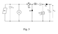
- FIG. 5 is an example disclosing a particular mode of realisation of the switches of the electric circuit according to the present invention.
- the switch S W14 of FIG. 5 is for example an IGBT transistor IG 1 .
- the first terminal of the switch S W14 is the collector of the IGBT transistor IG 1 .
- the emitter of the IGBT transistor IG 1 is the second terminal of the switch S W14 .
- the switch S W12 of FIG. 5 is a diode D 5 .
- the first terminal of the switch S W12 is the cathode of the diode D 5 and the second terminal of the switch S W12 is the anode of the diode D 5 .
- the switch S W13 of FIG. 5 is a NMOSFET M 3 .
- the first terminal of the switch S W13 is the drain of the NMOSFET M 3 .
- the second terminal of the switch S W13 is the source of the NMOSFET M 3 .
- FIG. 6 is an example of an algorithm for determining the maximum power point of the power source according to the present invention.
- the present algorithm is executed by the processor 300 .
- the algorithm for obtaining information enabling the determination of the maximum power point of the power source discharges the capacitor C UI in the inductor L 1 through interleaved sub-phases of partial charges and discharges prior to the monitoring of the voltage charge of the capacitor C UI in order to get information enabling the determination of the maximum power point of the power source.
- step S 600 the phase PH 1 starts.
- the phase PH 1 is shown in the FIGS. 7 a to 7 c.
- FIG. 7 a is an example of the power source voltage variations obtained according to the present invention.
- the time is represented on horizontal axis of the FIG. 7 a and the voltage is represented on the vertical axis of the FIG. 7 a.
- FIG. 7 b is an example of power source current variations obtained according to the present invention.
- the time is represented on horizontal axis of the FIG. 7 b and the current is represented on the vertical axis of the FIG. 7 b.
- FIG. 7 c is an example of the output voltage variations of the energy conversion device according to the present invention.
- the time is represented on horizontal axis of the FIG. 7 c and the voltage is represented on the vertical axis of the FIG. 7 c.
- the energy conversion device Conv acts as a boost converter.
- the NMOSFET M 3 and the diode D O are put in a conductive state and non conductive state according to a periodic pattern of which the duty cycle is adjusted in order to get a desired output voltage.
- the period of time wherein the command signal of the NMOSFET M 3 is high is named D.
- the period of time wherein the command signal of the NMOSFET M 3 is high is named (1 ⁇ D).
- the IGBT transistor IG 1 is always in conductive state, the NMOSFET M 3 is in conductive state during D and the diode D O is in conductive state during (1 ⁇ D).
- the diode D 5 is never in conductive state, the NMOSFET
- M 3 is not in conductive state during (1 ⁇ D) and the diode D O is not in conductive state during D.
- the voltage provided by the power source PV shown in FIG. 7 a corresponds to a voltage which corresponds to the MPP previously determined by the present algorithm.
- the current provided by the power source PV shown in FIG. 7 b is a current corresponding to the MPP previously determined by the present algorithm.
- the voltage V DC at the output shown in FIG. 7 c is a voltage obtained from the power source PV output voltage and the duty cycle.
- the current is provided to the load during the phase PH 1 .
- next step S 601 the processor 300 decides to interrupt the boost conversion mode in order to determine another MPP and moves to a phase PH 2 .
- phase PH 2 the capacitor C UI is discharged through the inductor L 1 through interleaved sub-phases of partial charges and discharges as shown in FIG. 7 a.
- phase PH 2 is decomposed into two sub-phases PH 2 a and PH 2 b and a maximum current is set in the sub-phase PH 2 a.
- Sub-phase PH 2 a represents the period of time in which the capacitor C UI is partially or completely discharged through the inductor L 1 .
- Sub-phase PH 2 b represents the period of time in which the inductor L 1 is partially or completely discharged on a storage device or the load and the capacitor C UI is partially charged by the power source.
- step S 602 the processor 300 starts the phase PH 2 a.
- the IGBT transistor IG 1 and the NMOSFET M 3 are set in the conductive state and the diodes D 5 and D O are in a non conductive state.
- the capacitor C UI transfers its energy into the inductor L 1 in a resonant way as it is shown in FIGS. 8 a and 8 b.
- FIG. 8 a is an example of variations of the current flowing through the inductor during the capacitor discharging phase, which is composed of several interleaved sub-phases of partial charges and discharges, according to the present invention.
- the time is represented on horizontal axis of the FIG. 8 a and the current is represented on the vertical axis of the FIG. 8 a.
- FIG. 8 b is an example of variations of the current flowing through the capacitor during the capacitor discharging phase, which is composed of several interleaved sub-phases of partial charges and discharges, according to the present invention.
- the time is represented on horizontal axis of the FIG. 8 b and the current is represented on the vertical axis of the FIG. 8 b.
- the processor 300 checks if the current I L1 flowing through the inductor L 1 is greater than a first predetermined value Thres 1 , for example equal to a maximum current of twenty Amps, or if the capacitor C UI is discharged.
- the capacitor C UI is considered to be discharged when the voltage V 1 is equal to a second predetermined value Thres 2 , which is for example equal to null value.
- step S 603 If the current I L1 flowing through the inductor L 1 is lower than or equal to the first predetermined value Thres 1 or if the capacitor C UI is not discharged, the processor 300 returns to step S 603 . Otherwise, the processor 300 moves to step S 604 .
- step S 604 the processor 300 starts the sub-phase PH 2 b.
- the IGBT transistor IG 1 and the NMOSFET M 3 are set in the not conductive state and the diodes D 5 and D O are in a conductive state.
- the inductor L 1 discharges its energy into the capacitor C O and also according to a particular feature into the load as it is shown in FIG. 8 a.
- the capacitance value of the capacitor C O is greater than the capacitance value of the capacitor C u , i.e. the inductor L 1 discharge happens much faster than the inductor L 1 charge meaning that the charge of the capacitor C UI is always much slower than its discharge, i.e. the inductor L 1 charge.
- the processor 300 checks if the current I L1 going through the inductor L 1 is smaller than a third predetermined value Thres 3 , for example equal to null value.
- step S 605 If the current I L1 going through the inductor L 1 is greater than the third predetermined value Thres 3 , the processor 300 returns to step S 605 . Otherwise, the processor 300 moves to step S 606 .
- the processor 300 checks if the voltage V 1 is greater than the second predetermined value Thres 2 , for example equal to null value.
- the processor 300 returns to step S 603 and executes successively the sub-phases PH 2 a and PH 2 b as far as the voltage V 1 is not smaller or equal to the predetermined value Thres 2 , for example null value.
- step S 607 If the voltage V 1 is smaller than or equal to the second predetermined value Thres 2 , the processor 300 moves to step S 607 .
- step S 607 the processor 300 starts the phase PH 3 .
- phase PH 3 the IGBT transistor IG 1 and the NMOSFET M 3 are set in the not conductive state and the diodes D 5 and D O are in a non conductive state.
- the capacitor C UI is charged from null voltage to open circuit voltage V OC as shown in FIG. 7 a and the current moves from the short circuit current to null value as shown in FIG. 7 b.
- the processor 300 commands the sampling, at the sampling period Tsamp, of the voltage V 1 which corresponds to the voltage on the capacitor C UI or of the power source PV.
- step S 609 the processor 300 gets all the samples determined at the previous step and processed according to the algorithm that will be disclosed in reference to the FIG. 9 and forms a curve as the one shown in FIG. 2 .
- the processor 300 determines the MPP thanks to the voltage and current values obtained from the algorithm of FIG. 9 by selecting the maximum power obtained from voltage and current values.
- step S 610 the phase PH 4 starts.
- the phase PH 4 is shown in the FIGS. 7 a to 7 c.
- phase PH 3 ends after a predetermined time duration or when the voltage derivative dV 1 /dt is equal to zero, meaning that the open circuit voltage V OC was reached.
- the energy conversion device acts as a boost converter.
- the NMOSFET M 3 and the diode D O are put in a conductive state and non conductive state according to a periodic pattern of which the duty cycle is adjusted in order to get a desired output voltage considering the newly determined MPP.
- the IGBT transistor IG 1 is in conductive state
- the NMOSFET M 3 is in conductive state during D
- the diode D O is in conductive state during (1 ⁇ D).
- the diode D 5 is not in conductive state
- the NMOSFET M 3 is not in conductive state during (1 ⁇ D)
- the diode D O is in conductive state during D.
- FIG. 9 is an example of an algorithm for determining the current and output voltage pairs of the power source in order to enable the determination of the maximum power point of the power source according to the mode of realisation of the present invention.
- the present algorithm is executed by the processor 300 .
- the algorithm for obtaining information enabling the determination of the maximum power point of the power source according to the particular mode of realisation of the present invention uses the voltage V 1 in order to determine the current going through the capacitor C UI during phase PH 3 .
- the current for the given sample is determined by multiplying the capacitance value of the capacitor C UI by the voltage derivative of the given sample, the voltage derivative being obtained through a fitted mathematical function, for example a polynomial function with real coefficients in order to filter the sampled voltages.
- Information enabling the determination of the maximum power point are the power-voltage droop characteristics of the power source PV, directly obtained from the current-voltage droop characteristics.
- each sample is a bi-dimensional vector the coefficients of which are the voltage value and time to which voltage has been measured.
- the processor 300 determines the size of a moving window.
- the size of the moving window indicates the number Npt of samples to be used for determining a curve based on the fitting of suitable mathematical functions, for example polynomial functions with real coefficients.
- the size of the moving window is odd. For example, the size of the moving window is equal to seventy one.
- the processor 300 determines the central point Nc of the moving window.
- step S 903 the processor 300 sets the variable i to the value Npt.
- step S 904 the processor 300 sets the variable j to i ⁇ Nc+1.
- step S 905 the processor 300 sets the variable k to one.
- step S 906 the processor 300 sets the value of x(k) to the time coefficient of sample j.
- step S 907 the processor 300 sets the value of y(k) to the voltage coefficient of sample j.
- step S 908 the processor 300 increments the variable k by one.
- step S 909 the processor 300 increments the variable j by one.
- the processor 300 checks if the variable j is strictly lower than the sum of i and Nc minored by one.
- step S 906 If the variable j is strictly lower than the sum of i and Nc minored by one, the processor 300 returns to step S 906 . Otherwise, the processor 300 moves to step S 911 .
- the processor 300 obtains then the a, b and c real coefficients of the second degree polynomial function ([a,b,c] ⁇ 3 ).
- the processor 300 evaluates the filtered voltage value and the current according to the following formulas:
- V PV (time[ i ]) a ⁇ time[ i] 2 +b ⁇ time[ i]+c
- I CUI (time[ i ]) C UI ⁇ ( a ⁇ time[ i]+b )
- step S 913 the processor 300 increments the variable i by one unit.
- the processor 300 checks if i is strictly lower than N minored by Nc wherein N is the total number of voltage samples obtained at step S 901 .
- the processor 300 If i is strictly lower than N minored by Nc, the processor 300 returns to step S 904 . Otherwise, the processor 300 interrupts the present algorithm and returns to step S 609 of the algorithm of FIG. 6 .
- step S 904 the processor 300 will displace the moving window by one sample.
Landscapes
- Engineering & Computer Science (AREA)
- Life Sciences & Earth Sciences (AREA)
- Sustainable Development (AREA)
- Sustainable Energy (AREA)
- Power Engineering (AREA)
- Physics & Mathematics (AREA)
- Electromagnetism (AREA)
- General Physics & Mathematics (AREA)
- Radar, Positioning & Navigation (AREA)
- Automation & Control Theory (AREA)
- Dc-Dc Converters (AREA)
- Control Of Electrical Variables (AREA)
Abstract
Description
- The present invention relates generally to an apparatus and a method for obtaining information enabling the determination of a characteristic like the maximum power point of a power source like a photovoltaic cell or an array of cells or a fuel cell.
- A photovoltaic cell directly converts solar energy into electrical energy. The electrical energy produced by the photovoltaic cell can be extracted over time and used in the form of electric power. The direct electric power provided by the photovoltaic cell is provided to conversion devices like DC-DC up/down converter circuits and/or DC/AC inverter circuits.
- However, the current-voltage droop characteristics of photovoltaic cells cause the output power to change nonlinearly with the current drawn from photovoltaic cells. The power-voltage curve changes according to climatic variations like light radiation levels and operation temperatures.
- The near optimal point at which to operate photovoltaic cells or arrays of cells is at or near the region of the current-voltage curve where power is greatest. This point is denominated as the Maximum Power Point (MPP).
- It is important to operate the photovoltaic cells around the MPP to optimize their power generation efficiency.
- As the power-voltage curve changes according to climatic variations, the MPP also changes according to climatic variations.
- It is then necessary to be able to identify the MPP at any time.
- The present invention aims at providing an apparatus which enables to obtain information representative of the output current and voltage variations of the power source, for example an array of photovoltaic cells, in order to determine its maximum power point.
- To that end, the present invention concerns an apparatus for obtaining information enabling the determination of a characteristic like the maximum power point of a power source, the apparatus comprising at least an inductor and a capacitor, the information enabling the determination of the characteristic of the power source being obtained by monitoring the voltage charge of the capacitor, characterised in that the apparatus for obtaining information enabling the determination of the characteristic of the power source comprises means for discharging the capacitor through the inductor prior to the monitoring of the capacitor charge.
- The present invention concerns also a method for obtaining information enabling the determination of a characteristic like the maximum power point of a power source connected to a direct current converter, the direct current converter comprising at least an inductor and a capacitor, characterised in that the method comprises the steps of:
-
- discharging the capacitor through the inductor,
- monitoring the voltage charge of the capacitor in order to obtain information enabling the determination of the characteristic of the power source.
- Thus, it is possible to obtain information representative of the output current and voltage variations of the power source, for example, in order to determine the MPP or to determine a fault of the power source or to determine a fill factor of the power source.
- Furthermore, in most of DC/DC and/or DC/AC converters, the capacitor and the inductor are already available for conversion purpose. The capacitor and the inductor can be also used for monitoring the voltage and current variations during at least one particular period of time. The monitored voltage and current variations enable the obtaining of information like the wanted voltage-current/voltage-power droop characteristics of the power source at any time. The present invention avoids to add any other extra inductor or capacitor to the system.
- According to a particular feature, the apparatus comprises means for monitoring the current flowing through the inductor during the discharge of the capacitor and the capacitor is discharged in the inductor as long as the current flowing through the inductor reaches a first predetermined current value or as long as the capacitor is not discharged.
- Thus, it is possible to limit the current levels on both the inductor and capacitor, avoiding large current peaks due to the resonance between the inductor and the capacitor, which may cause the saturation of the inductor magnetic core and also decrease the lifetime of the capacitor.
- According to a particular feature, the apparatus comprises means for discharging the inductor into at least another device once the current flowing through the inductor value reaches the first predetermined value or once the capacitor is discharged.
- According to a particular feature, the other device is an energy storage device or a load.
- Thus, the energy stored in the inductor is not dissipated in any resistive component but it is exchanged with other storage devices such as a capacitor or even directly supplied to the load, resulting in a non-dissipative procedure. There is no power interruption from the power source side, since during the inductor discharge the power source continues to store power into the input capacitor.
- According to a particular feature, the apparatus comprises means for obtaining the current outputted by the power source during the monitoring of the charge of the capacitor.
- Thus, it is possible to obtain the whole voltage-current/voltage-power droop characteristics of the power source from null voltage value up to the open-circuit voltage value.
- According to a particular feature, the current outputted by the power source is obtained from a current sensor or derived from the voltage values obtained during the monitoring of the charge of the capacitor.
- Thus, the implementation cost may not be increased if the current sensor is not available. Finally, no additional component is needed at all to implement this technique.
- According to a particular feature, the discharge of the capacitor through the inductor and the discharge of the inductor are executed iteratively as far as the voltage of the capacitor reaches a second predetermined value.
- Thus, the capacitor discharge can happen in a non dissipative way, meaning that the energy which was stored in the capacitor is completely given to the load, reducing the drawbacks of stopping the power source supply during this small period of time when this energy is dissipated in a resistor, for example.
- The present invention concerns also a direct current converter characterised in that it comprises the apparatus for obtaining information enabling the determination of the maximum power point of a power source.
- Thus, it is possible to obtain information representative of the output current and voltage variations of the power source, for example an array of photovoltaic cells, in order to determine the MPP.
- Furthermore, in most of DC/DC and/or DC/AC converters, the capacitor and the inductor are already available for conversion purpose. The capacitor and the inductor can also be used for monitoring the voltage and current variations during at least one particular period of time. The monitored voltage and current variations enable the obtaining of information like the wanted voltage-current/voltage-power droop characteristics of the power source at any time. The present invention avoids to add any other extra inductor or capacitor to the system.
- The characteristics of the invention will emerge more clearly from a reading of the following description of an example embodiment, the said description being produced with reference to the accompanying drawings, among which:
-
FIG. 1 is an example of an energy conversion system wherein the present invention may be implemented; -
FIG. 2 is an example of a curve representing the output current variations of a power source according to the output voltage of the power source; -
FIG. 3 represents an example of a device comprising an energy conversion device according to the present invention; -
FIG. 4 is an example of an energy conversion device comprising an inductor and a capacitor according to the present invention in order to obtain information enabling the determination of the maximum power point of the power source; -
FIG. 5 is an example disclosing a particular mode of realisation of the switches of the electric circuit according to the present invention; -
FIG. 6 is an example of an algorithm for determining the maximum power point of the power source according to the present invention; -
FIG. 7 a is an example of the power source voltage variations obtained according to the present invention; -
FIG. 7 b is an example of power source current variations obtained according to the present invention; -
FIG. 7 c is an example of the output voltage variations of the energy conversion device according to the present invention; -
FIG. 8 a is an example of variations of the current flowing through the inductor during the capacitor discharging phase, which is composed of several interleaved sub-phases of partial charges and discharges, according to the present invention; -
FIG. 8 b is an example of variations of the current flowing through the capacitor during the capacitor discharging phase, which is composed of several interleaved sub-phases of partial charges and discharges, according to the present invention; -
FIG. 9 is an example of an algorithm for determining the output current and output voltage pairs of the power source in order to enable the determination of the maximum power point of the power source according to the mode of realisation of the present invention. -
FIG. 1 is an example of an energy conversion system wherein the present invention may be implemented. - The energy conversion system is composed of a power source PV like a photovoltaic cell or an array of cells or a fuel cell connected to an energy conversion device Conv like a DC-DC step-down/step-up converter and/or a DC/AC converter also named inverter, which output provides electrical energy to the load Lo.
- The power source PV provides current intended to the load Lo. The current is converted by the conversion device Conv prior to be used by the load Lo.
-
FIG. 2 is an example of a curve representing the output current variations of a power source according to the output voltage of the power source. - On the horizontal axis of
FIG. 2 , voltage values are shown. The voltage values are comprised between null value and the open circuit voltage VOC. - On the vertical axis of
FIG. 2 , current values are shown. The current values are comprised between null value and the short circuit current ISC. - At any given light level and photovoltaic array temperature there is an infinite number of current-voltage pairs, or operating points, at which the photovoltaic array can operate. However, there exists a single MPP for a given light level and photovoltaic array temperature.
-
FIG. 3 represents an example of a device comprising an energy conversion device according to the present invention. - The energy conversion device Conv has, for example, an architecture based on components connected together by a
bus 301 and aprocessor 300 controlled by the programs related to the algorithms as disclosed in theFIGS. 6 and 9 . - It has to be noted here that the energy conversion device Conv is, in a variant, implemented under the form of one or several dedicated integrated circuits which execute the same operations as the one executed by the
processor 300 as disclosed hereinafter. - The
bus 301 links theprocessor 300 to a read onlymemory ROM 302, a randomaccess memory RAM 303, an analogue todigital converter ADC 306 and theelectric circuit 305 according to the invention. - The read only
memory ROM 302 contains instructions of the programs related to the algorithms as disclosed in theFIGS. 6 and 9 which are transferred, when the energy conversion device Conv is powered on to the randomaccess memory RAM 303. - The
RAM memory 303 contains registers intended to receive variables, and the instructions of the programs related to the algorithms as disclosed in theFIGS. 6 and 9 . - The analogue to
digital converter 306 is connected to theelectric circuit 305 according to the invention which forms the power stage and converts voltages and currents if needed into binary information. -
FIG. 4 is an example of an electric circuit comprising an inductor and a capacitor according to the present invention in order to obtain information enabling the determination of the maximum power point of the power source. - The electric circuit is a merged buck/boost converter which is able, according to the state of switches, to operate in a buck mode (step-down mode) or in a boost mode (step-up mode), without inverting the output voltage polarity as it is done with the classical buck-boost converter.
- The electric circuit according to the present invention comprises an input filter capacitor CUI, the positive terminal of which is connected to the positive terminal of the power source PV. The negative terminal of the capacitor CUI is connected to the negative terminal of the power source PV. Voltage measurement means measure the voltage V1 on the capacitor CUI and on inductor L1 when the latter one is connected in parallel with the power source.
- The positive terminal of the capacitor CUI is connected to a first terminal of a switch SW14.
- The second terminal of switch SW14 is connected to a first terminal of a switch SW12 and to a first terminal of an inductor L1.
- The second terminal of a switch SW12 is connected to the negative terminal of the power source PV.
- The second terminal of the inductor L1 is connected to a first terminal of current measurement means.
- The second terminal of current measurement means A is connected to the anode of a diode DO and to a first terminal of a switch SW13. The second terminal of the switch SW13 is connected to the negative terminal of the power source PV.
- The cathode of the diode DO is connected to the positive terminal of a capacitor CO and the negative terminal of the capacitor CO is connected to the negative terminal of the power source PV.
- When the merged buck/boost converter operates in buck mode, the switch SW13 is always in OFF state and diode DO is always in conductive state.
- The switch SW14 is put in a conductive state according to a periodic pattern of which the duty cycle is adjusted in order to get a desired output voltage VDC. The period of time the switch SW14 is high is named D. The period of time wherein the command signal of the switch SW14 is low is named (1−D).
- The switch SW12 is in non conductive state during D and is in conductive state during (1−D).
- When the merged buck/boost converter operates in boost mode, the switch SW14 is always in conductive state and the switch SW12 is never in conductive state.
- The switch SW13 is in conductive state during D and is in non conductive state during (1−D).
-
FIG. 5 is an example disclosing a particular mode of realisation of the switches of the electric circuit according to the present invention. - The switch SW14 of
FIG. 5 is for example an IGBT transistor IG1. The first terminal of the switch SW14 is the collector of the IGBT transistor IG1. The emitter of the IGBT transistor IG1 is the second terminal of the switch SW14. - The switch SW12 of
FIG. 5 is a diode D5. The first terminal of the switch SW12 is the cathode of the diode D5 and the second terminal of the switch SW12 is the anode of the diode D5. - The switch SW13 of
FIG. 5 is a NMOSFET M3. The first terminal of the switch SW13 is the drain of the NMOSFET M3. The second terminal of the switch SW13 is the source of the NMOSFET M3. -
FIG. 6 is an example of an algorithm for determining the maximum power point of the power source according to the present invention. - More precisely, the present algorithm is executed by the
processor 300. - The algorithm for obtaining information enabling the determination of the maximum power point of the power source discharges the capacitor CUI in the inductor L1 through interleaved sub-phases of partial charges and discharges prior to the monitoring of the voltage charge of the capacitor CUI in order to get information enabling the determination of the maximum power point of the power source.
- At step S600, the phase PH1 starts. The phase PH1 is shown in the
FIGS. 7 a to 7 c. -
FIG. 7 a is an example of the power source voltage variations obtained according to the present invention. - The time is represented on horizontal axis of the
FIG. 7 a and the voltage is represented on the vertical axis of theFIG. 7 a. -
FIG. 7 b is an example of power source current variations obtained according to the present invention. - The time is represented on horizontal axis of the
FIG. 7 b and the current is represented on the vertical axis of theFIG. 7 b. -
FIG. 7 c is an example of the output voltage variations of the energy conversion device according to the present invention. - The time is represented on horizontal axis of the
FIG. 7 c and the voltage is represented on the vertical axis of theFIG. 7 c. - During the phase PH1, the energy conversion device Conv acts as a boost converter. The NMOSFET M3 and the diode DO are put in a conductive state and non conductive state according to a periodic pattern of which the duty cycle is adjusted in order to get a desired output voltage. The period of time wherein the command signal of the NMOSFET M3 is high is named D. The period of time wherein the command signal of the NMOSFET M3 is high is named (1−D).
- During the phase PH1, the IGBT transistor IG1 is always in conductive state, the NMOSFET M3 is in conductive state during D and the diode DO is in conductive state during (1−D).
- During the phase PH1, the diode D5 is never in conductive state, the NMOSFET
- M3 is not in conductive state during (1−D) and the diode DO is not in conductive state during D.
- The voltage provided by the power source PV shown in
FIG. 7 a corresponds to a voltage which corresponds to the MPP previously determined by the present algorithm. - The current provided by the power source PV shown in
FIG. 7 b is a current corresponding to the MPP previously determined by the present algorithm. - The voltage VDC at the output shown in
FIG. 7 c is a voltage obtained from the power source PV output voltage and the duty cycle. - The current is provided to the load during the phase PH1.
- At next step S601, the
processor 300 decides to interrupt the boost conversion mode in order to determine another MPP and moves to a phase PH2. - In phase PH2, the capacitor CUI is discharged through the inductor L1 through interleaved sub-phases of partial charges and discharges as shown in
FIG. 7 a. - In order to avoid that high current flows through L1 and/or CUI the phase PH2 is decomposed into two sub-phases PH2 a and PH2 b and a maximum current is set in the sub-phase PH2 a.
- Sub-phase PH2 a represents the period of time in which the capacitor CUI is partially or completely discharged through the inductor L1.
- Sub-phase PH2 b represents the period of time in which the inductor L1 is partially or completely discharged on a storage device or the load and the capacitor CUI is partially charged by the power source.
- At next step S602, the
processor 300 starts the phase PH2 a. - In sub-phase PH2 a, the IGBT transistor IG1 and the NMOSFET M3 are set in the conductive state and the diodes D5 and DO are in a non conductive state.
- During sub-phase PH2 a, the capacitor CUI transfers its energy into the inductor L1 in a resonant way as it is shown in
FIGS. 8 a and 8 b. -
FIG. 8 a is an example of variations of the current flowing through the inductor during the capacitor discharging phase, which is composed of several interleaved sub-phases of partial charges and discharges, according to the present invention. - The time is represented on horizontal axis of the
FIG. 8 a and the current is represented on the vertical axis of theFIG. 8 a. -
FIG. 8 b is an example of variations of the current flowing through the capacitor during the capacitor discharging phase, which is composed of several interleaved sub-phases of partial charges and discharges, according to the present invention. - The time is represented on horizontal axis of the
FIG. 8 b and the current is represented on the vertical axis of theFIG. 8 b. - At next step S603, the
processor 300 checks if the current IL1 flowing through the inductor L1 is greater than a first predetermined value Thres1, for example equal to a maximum current of twenty Amps, or if the capacitor CUI is discharged. - The capacitor CUI is considered to be discharged when the voltage V1 is equal to a second predetermined value Thres2, which is for example equal to null value.
- If the current IL1 flowing through the inductor L1 is lower than or equal to the first predetermined value Thres1 or if the capacitor CUI is not discharged, the
processor 300 returns to step S603. Otherwise, theprocessor 300 moves to step S604. - As it can be seen if
FIG. 8 a, up to time T1, the current IL1 going through the inductor L1 reaches the maximum current of 20 Amp several times. - At T2, the capacitor CUI is discharged.
- At step S604, the
processor 300 starts the sub-phase PH2 b. - In sub-phase PH2 b, the IGBT transistor IG1 and the NMOSFET M3 are set in the not conductive state and the diodes D5 and DO are in a conductive state.
- The inductor L1 discharges its energy into the capacitor CO and also according to a particular feature into the load as it is shown in
FIG. 8 a. - At the same time the capacitor CUI is charged by the power source PV as shown in
FIG. 8 b. - It has to be noted here that the capacitance value of the capacitor CO is greater than the capacitance value of the capacitor Cu, i.e. the inductor L1 discharge happens much faster than the inductor L1 charge meaning that the charge of the capacitor CUI is always much slower than its discharge, i.e. the inductor L1 charge.
- At next step S605, the
processor 300 checks if the current IL1 going through the inductor L1 is smaller than a third predetermined value Thres3, for example equal to null value. - If the current IL1 going through the inductor L1 is greater than the third predetermined value Thres3, the
processor 300 returns to step S605. Otherwise, theprocessor 300 moves to step S606. - At next step S606, the
processor 300 checks if the voltage V1 is greater than the second predetermined value Thres2, for example equal to null value. - If the voltage V1 is upper than the second predetermined value Thres2, the
processor 300 returns to step S603 and executes successively the sub-phases PH2 a and PH2 b as far as the voltage V1 is not smaller or equal to the predetermined value Thres2, for example null value. - If the voltage V1 is smaller than or equal to the second predetermined value Thres2, the
processor 300 moves to step S607. - At step S607, the
processor 300 starts the phase PH3. - In phase PH3, the IGBT transistor IG1 and the NMOSFET M3 are set in the not conductive state and the diodes D5 and DO are in a non conductive state.
- The capacitor CUI is charged from null voltage to open circuit voltage VOC as shown in
FIG. 7 a and the current moves from the short circuit current to null value as shown inFIG. 7 b. - At next step S608, the
processor 300 commands the sampling, at the sampling period Tsamp, of the voltage V1 which corresponds to the voltage on the capacitor CUI or of the power source PV. - At step S609, the
processor 300 gets all the samples determined at the previous step and processed according to the algorithm that will be disclosed in reference to theFIG. 9 and forms a curve as the one shown inFIG. 2 . - At the same step, the
processor 300 determines the MPP thanks to the voltage and current values obtained from the algorithm ofFIG. 9 by selecting the maximum power obtained from voltage and current values. - At step S610, the phase PH4 starts. The phase PH4 is shown in the
FIGS. 7 a to 7 c. - It has to be noted here that the phase PH3 ends after a predetermined time duration or when the voltage derivative dV1/dt is equal to zero, meaning that the open circuit voltage VOC was reached.
- During the phase PH4, the energy conversion device acts as a boost converter. The NMOSFET M3 and the diode DO are put in a conductive state and non conductive state according to a periodic pattern of which the duty cycle is adjusted in order to get a desired output voltage considering the newly determined MPP. During the phase PH4, the IGBT transistor IG1 is in conductive state, the NMOSFET M3 is in conductive state during D and the diode DO is in conductive state during (1−D).
- During the phase PH4, the diode D5 is not in conductive state, the NMOSFET M3 is not in conductive state during (1−D) and the diode DO is in conductive state during D.
-
FIG. 9 is an example of an algorithm for determining the current and output voltage pairs of the power source in order to enable the determination of the maximum power point of the power source according to the mode of realisation of the present invention. - More precisely, the present algorithm is executed by the
processor 300. - The algorithm for obtaining information enabling the determination of the maximum power point of the power source according to the particular mode of realisation of the present invention uses the voltage V1 in order to determine the current going through the capacitor CUI during phase PH3.
- From a general point of view, with the present algorithm, the current for the given sample is determined by multiplying the capacitance value of the capacitor CUI by the voltage derivative of the given sample, the voltage derivative being obtained through a fitted mathematical function, for example a polynomial function with real coefficients in order to filter the sampled voltages.
- The fitted mathematical function is obtained by minimizing the sum of the squares of the difference between the measured voltage yi with i=1 to N at consecutive time samples xi and mathematical functions f(xi) in order to obtain a processed voltage for the given time sample. It is done as follows.
- Given N samples (x1,y1), (x2,y2) . . . (xN,yN), the required fitted mathematical function can be written, for example, in the form:
-
f(x)=C 1 ·f 1(x)+C 2 ·f 2(x)+ . . . +C K ·f K(x) - where fj(x), j=1, 2 . . . K are mathematical functions of x and the Cj, j=1, 2 . . . K are constants which are initially unknown.
- The sum of the squares of the difference between f(x) and the actual values of y is given by
-
- This error term is minimized by taking the partial first derivative of E with respect to each of constants, Cj, j=1, 2, . . . K and putting the result to zero. Thus, a symmetric system of K linear equation is obtained and solved for C1, C2, . . . , CK. This procedure is also known as Least Mean Squares (LMS) algorithm.
- Information enabling the determination of the maximum power point are the power-voltage droop characteristics of the power source PV, directly obtained from the current-voltage droop characteristics.
- With the voltage samples of V1, a curve is obtained based on the fitting of suitable mathematical functions, for example polynomial functions with real coefficients, in pre-defined windows which will move for each sample. Thus, the voltage is filtered and its derivative can be simultaneously calculated for every central point in the window in a very simple and direct way, resulting in the determination of current without the need of any additional current sensor.
- At next step S900, the
processor 300 gets the samples obtained during phase PH3. Each sample is a bi-dimensional vector the coefficients of which are the voltage value and time to which voltage has been measured. - At next step S901, the
processor 300 determines the size of a moving window. The size of the moving window indicates the number Npt of samples to be used for determining a curve based on the fitting of suitable mathematical functions, for example polynomial functions with real coefficients. The size of the moving window is odd. For example, the size of the moving window is equal to seventy one. - At next step S902, the
processor 300 determines the central point Nc of the moving window. - At next step S903, the
processor 300 sets the variable i to the value Npt. - At next step S904, the
processor 300 sets the variable j to i−Nc+ 1. - At next step S905, the
processor 300 sets the variable k to one. - At next step S906, the
processor 300 sets the value of x(k) to the time coefficient of sample j. - At next step S907, the
processor 300 sets the value of y(k) to the voltage coefficient of sample j. - At next step S908, the
processor 300 increments the variable k by one. - At next step S909, the
processor 300 increments the variable j by one. - At next step S910, the
processor 300 checks if the variable j is strictly lower than the sum of i and Nc minored by one. - If the variable j is strictly lower than the sum of i and Nc minored by one, the
processor 300 returns to step S906. Otherwise, theprocessor 300 moves to step S911. - At step S911, the
processor 300 determines the fitted mathematical function, for example the polynomial function y(x)=ax2+bx+c, using the Least Mean Square algorithm and all the x(k) and y(k) values sampled at steps S906 and S907 until the condition on S910 is reached. - The
processor 300 obtains then the a, b and c real coefficients of the second degree polynomial function ([a,b,c] ε3).
- At next step S912, the
processor 300 evaluates the filtered voltage value and the current according to the following formulas: -
V PV(time[i])=a·time[i] 2 +b·time[i]+c -
I CUI(time[i])=C UI·(a·time[i]+b) - At next step S913, the
processor 300 increments the variable i by one unit. - At next step S914, the
processor 300 checks if i is strictly lower than N minored by Nc wherein N is the total number of voltage samples obtained at step S901. - If i is strictly lower than N minored by Nc, the
processor 300 returns to step S904. Otherwise, theprocessor 300 interrupts the present algorithm and returns to step S609 of the algorithm ofFIG. 6 . - By moving to step S904, the
processor 300 will displace the moving window by one sample. - Naturally, many modifications can be made to the embodiments of the invention described above without departing from the scope of the present invention.
Claims (11)
Applications Claiming Priority (4)
| Application Number | Priority Date | Filing Date | Title |
|---|---|---|---|
| EP09179087.3 | 2009-12-14 | ||
| EP09179087A EP2333634A1 (en) | 2009-12-14 | 2009-12-14 | Method for obtaining information enabling the determination of a characteristic of a power source |
| EP09179087 | 2009-12-14 | ||
| PCT/EP2010/069210 WO2011073069A1 (en) | 2009-12-14 | 2010-12-08 | Method for obtaining information enabling the determination of a characteristic of a power source |
Publications (2)
| Publication Number | Publication Date |
|---|---|
| US20120249167A1 true US20120249167A1 (en) | 2012-10-04 |
| US9310821B2 US9310821B2 (en) | 2016-04-12 |
Family
ID=42110023
Family Applications (1)
| Application Number | Title | Priority Date | Filing Date |
|---|---|---|---|
| US13/515,523 Expired - Fee Related US9310821B2 (en) | 2009-12-14 | 2010-12-08 | Method for obtaining information enabling the determination of a characteristic of a power source |
Country Status (5)
| Country | Link |
|---|---|
| US (1) | US9310821B2 (en) |
| EP (2) | EP2333634A1 (en) |
| JP (1) | JP6012470B2 (en) |
| CN (1) | CN102667659B (en) |
| WO (1) | WO2011073069A1 (en) |
Cited By (1)
| Publication number | Priority date | Publication date | Assignee | Title |
|---|---|---|---|---|
| US20140067298A1 (en) * | 2012-09-04 | 2014-03-06 | Texas Instruments Incorporated | Noninvasive monitoring of a photovoltaic system |
Families Citing this family (1)
| Publication number | Priority date | Publication date | Assignee | Title |
|---|---|---|---|---|
| JP5432937B2 (en) * | 2011-02-23 | 2014-03-05 | 株式会社日立パワーソリューションズ | Solar cell characteristic acquisition circuit and solar cell control device |
Citations (4)
| Publication number | Priority date | Publication date | Assignee | Title |
|---|---|---|---|---|
| US5381327A (en) * | 1992-03-19 | 1995-01-10 | Astec International, Ltd. | Electrical power inverter |
| US5932994A (en) * | 1996-05-15 | 1999-08-03 | Samsung Electronics, Co., Ltd. | Solar cell power source device |
| US6111767A (en) * | 1998-06-22 | 2000-08-29 | Heliotronics, Inc. | Inverter integrated instrumentation having a current-voltage curve tracer |
| US20100046250A1 (en) * | 2008-08-20 | 2010-02-25 | Ricoh Company, Ltd. | Dc-dc converter |
Family Cites Families (13)
| Publication number | Priority date | Publication date | Assignee | Title |
|---|---|---|---|---|
| JP3373896B2 (en) * | 1993-07-06 | 2003-02-04 | 三洋電機株式会社 | Solar power |
| JP3439876B2 (en) * | 1995-04-26 | 2003-08-25 | 京セラ株式会社 | Solar power generator |
| JP3554116B2 (en) * | 1996-09-06 | 2004-08-18 | キヤノン株式会社 | Power control device and solar power generation system using the same |
| CN2514538Y (en) * | 2001-11-12 | 2002-10-02 | 武汉加伟光电科技有限公司 | Automatic power servo unit for solar battery |
| JP4294346B2 (en) * | 2003-03-13 | 2009-07-08 | 一隆 板子 | Photovoltaic power generation system and its maximum power point tracking control method |
| US20060132102A1 (en) * | 2004-11-10 | 2006-06-22 | Harvey Troy A | Maximum power point tracking charge controller for double layer capacitors |
| EP1821386A2 (en) * | 2006-02-17 | 2007-08-22 | Power Systems Co., Ltd. | Charging apparatus for capacitor storage type power source and discharging apparatus for capacitor storage type power source |
| JP2008046751A (en) * | 2006-08-11 | 2008-02-28 | Toyota Motor Corp | SOLAR POWER GENERATION SYSTEM, VEHICLE, SOLAR POWER GENERATION SYSTEM CONTROL METHOD, AND COMPUTER-READABLE RECORDING MEDIUM RECORDING PROGRAM FOR CAUSING COMPUTER TO EXECUTE THE CONTROL METHOD |
| JP5291896B2 (en) * | 2007-06-01 | 2013-09-18 | Jx日鉱日石エネルギー株式会社 | Power conditioner for photovoltaic power generation, photovoltaic power generation system, and output power control method for photovoltaic power generation system |
| JP5322256B2 (en) * | 2007-11-07 | 2013-10-23 | 学校法人東京電機大学 | Photovoltaic power generation control device and power evaluation method in solar power generation control |
| US7969133B2 (en) * | 2008-05-14 | 2011-06-28 | National Semiconductor Corporation | Method and system for providing local converters to provide maximum power point tracking in an energy generating system |
| CN101282044B (en) * | 2008-05-30 | 2010-06-23 | 东莞市特龙金科能源科技有限公司 | Solar cell matching circuit and its realization method |
| EP2280329A1 (en) | 2009-07-10 | 2011-02-02 | Mitsubishi Electric R&D Centre Europe B.V. | Apparatus for obtaining information enabling the determination of the maximum power point of a power source. |
-
2009
- 2009-12-14 EP EP09179087A patent/EP2333634A1/en not_active Withdrawn
-
2010
- 2010-12-08 WO PCT/EP2010/069210 patent/WO2011073069A1/en not_active Ceased
- 2010-12-08 EP EP10790551.5A patent/EP2513737B1/en not_active Not-in-force
- 2010-12-08 US US13/515,523 patent/US9310821B2/en not_active Expired - Fee Related
- 2010-12-08 JP JP2012543605A patent/JP6012470B2/en not_active Expired - Fee Related
- 2010-12-08 CN CN201080056568.5A patent/CN102667659B/en not_active Expired - Fee Related
Patent Citations (4)
| Publication number | Priority date | Publication date | Assignee | Title |
|---|---|---|---|---|
| US5381327A (en) * | 1992-03-19 | 1995-01-10 | Astec International, Ltd. | Electrical power inverter |
| US5932994A (en) * | 1996-05-15 | 1999-08-03 | Samsung Electronics, Co., Ltd. | Solar cell power source device |
| US6111767A (en) * | 1998-06-22 | 2000-08-29 | Heliotronics, Inc. | Inverter integrated instrumentation having a current-voltage curve tracer |
| US20100046250A1 (en) * | 2008-08-20 | 2010-02-25 | Ricoh Company, Ltd. | Dc-dc converter |
Cited By (2)
| Publication number | Priority date | Publication date | Assignee | Title |
|---|---|---|---|---|
| US20140067298A1 (en) * | 2012-09-04 | 2014-03-06 | Texas Instruments Incorporated | Noninvasive monitoring of a photovoltaic system |
| US9270226B2 (en) * | 2012-09-04 | 2016-02-23 | Texas Instruments Incorporated | Noninvasive monitoring of a photovoltaic system |
Also Published As
| Publication number | Publication date |
|---|---|
| JP2013513878A (en) | 2013-04-22 |
| CN102667659B (en) | 2015-10-14 |
| EP2513737A1 (en) | 2012-10-24 |
| JP6012470B2 (en) | 2016-10-25 |
| WO2011073069A1 (en) | 2011-06-23 |
| EP2333634A1 (en) | 2011-06-15 |
| CN102667659A (en) | 2012-09-12 |
| US9310821B2 (en) | 2016-04-12 |
| EP2513737B1 (en) | 2018-07-18 |
Similar Documents
| Publication | Publication Date | Title |
|---|---|---|
| US20120139504A1 (en) | Apparatus for obtaining information enabling the determination of the maximum power point of a power source | |
| US9966899B2 (en) | Systems and methods for controlling maximum power point tracking controllers | |
| US9086716B2 (en) | Method for obtaining information enabling the determination of a characteristic of a power source | |
| Zhang et al. | A CMOS-Based energy harvesting approach for laterally arrayed multibandgap concentrated photovoltaic systems | |
| Zengin | A hybrid current modulated DAB DC/DC converter for connecting PV modules to DC grid considering partial shading | |
| US9310821B2 (en) | Method for obtaining information enabling the determination of a characteristic of a power source | |
| Shao et al. | A new maximum power point tracking method for photovoltaic arrays using golden section search algorithm | |
| EP2722725B1 (en) | Device for tracking a maximum power point of a power source | |
| Azzouzi | Optimization of photovoltaic generator by using PO algorithm under different weather conditions | |
| EP2515423A1 (en) | Apparatus for controlling the current going through an inductor of an energy conversion device | |
| EP2273659A1 (en) | Method and an apparatus for obtaining information enabling the determination of the maximum power point of a power source | |
| EP2533127A1 (en) | Apparatus for obtaining information enabling the determination of a characteristic like the maximum power point of a power source | |
| EP2450769B1 (en) | Device for tracking a maximum power point of a power source | |
| Aissani et al. | Small-Signal Modeling and Voltage PID controller-Synthesis for Cascade Regulation of Renewable Energy Conversion System | |
| Jantharamin et al. | Model-based maximum power point tracking | |
| Toumi et al. | Energy Reports | |
| Hadi et al. | Optimized photovoltaic pumping system with DC-DC converter | |
| Elangovan et al. | IMPLEMENTATION OF MPPT ALGORITHM FOR SOLAR PHOTOVOLTAIC CELL USING INCREMENTAL CONDUCTANCE METHOD | |
| Ranjan | Modelling and Simulation of a Photovoltaic System with MPPT Controller | |
| JP2016139378A (en) | Photocell operating point control method, photocell system and control method thereof |
Legal Events
| Date | Code | Title | Description |
|---|---|---|---|
| AS | Assignment |
Owner name: MITSUBISHI ELECTRIC CORPORATION, JAPAN Free format text: ASSIGNMENT OF ASSIGNORS INTEREST;ASSIGNOR:BUIATTI, GUSTAVO;REEL/FRAME:028400/0413 Effective date: 20120430 |
|
| STCF | Information on status: patent grant |
Free format text: PATENTED CASE |
|
| MAFP | Maintenance fee payment |
Free format text: PAYMENT OF MAINTENANCE FEE, 4TH YEAR, LARGE ENTITY (ORIGINAL EVENT CODE: M1551); ENTITY STATUS OF PATENT OWNER: LARGE ENTITY Year of fee payment: 4 |
|
| FEPP | Fee payment procedure |
Free format text: MAINTENANCE FEE REMINDER MAILED (ORIGINAL EVENT CODE: REM.); ENTITY STATUS OF PATENT OWNER: LARGE ENTITY |
|
| LAPS | Lapse for failure to pay maintenance fees |
Free format text: PATENT EXPIRED FOR FAILURE TO PAY MAINTENANCE FEES (ORIGINAL EVENT CODE: EXP.); ENTITY STATUS OF PATENT OWNER: LARGE ENTITY |
|
| STCH | Information on status: patent discontinuation |
Free format text: PATENT EXPIRED DUE TO NONPAYMENT OF MAINTENANCE FEES UNDER 37 CFR 1.362 |
|
| FP | Lapsed due to failure to pay maintenance fee |
Effective date: 20240412 |