US20120249108A1 - Constant frequency on-time control system and method and voltage regulator using the same - Google Patents
Constant frequency on-time control system and method and voltage regulator using the same Download PDFInfo
- Publication number
- US20120249108A1 US20120249108A1 US13/181,686 US201113181686A US2012249108A1 US 20120249108 A1 US20120249108 A1 US 20120249108A1 US 201113181686 A US201113181686 A US 201113181686A US 2012249108 A1 US2012249108 A1 US 2012249108A1
- Authority
- US
- United States
- Prior art keywords
- time
- setting parameter
- frequency setting
- voltage
- frequency
- Prior art date
- Legal status (The legal status is an assumption and is not a legal conclusion. Google has not performed a legal analysis and makes no representation as to the accuracy of the status listed.)
- Granted
Links
Images


Classifications
-
- H—ELECTRICITY
- H02—GENERATION; CONVERSION OR DISTRIBUTION OF ELECTRIC POWER
- H02M—APPARATUS FOR CONVERSION BETWEEN AC AND AC, BETWEEN AC AND DC, OR BETWEEN DC AND DC, AND FOR USE WITH MAINS OR SIMILAR POWER SUPPLY SYSTEMS; CONVERSION OF DC OR AC INPUT POWER INTO SURGE OUTPUT POWER; CONTROL OR REGULATION THEREOF
- H02M3/00—Conversion of DC power input into DC power output
- H02M3/02—Conversion of DC power input into DC power output without intermediate conversion into AC
- H02M3/04—Conversion of DC power input into DC power output without intermediate conversion into AC by static converters
- H02M3/10—Conversion of DC power input into DC power output without intermediate conversion into AC by static converters using discharge tubes with control electrode or semiconductor devices with control electrode
- H02M3/145—Conversion of DC power input into DC power output without intermediate conversion into AC by static converters using discharge tubes with control electrode or semiconductor devices with control electrode using devices of a triode or transistor type requiring continuous application of a control signal
- H02M3/155—Conversion of DC power input into DC power output without intermediate conversion into AC by static converters using discharge tubes with control electrode or semiconductor devices with control electrode using devices of a triode or transistor type requiring continuous application of a control signal using semiconductor devices only
- H02M3/156—Conversion of DC power input into DC power output without intermediate conversion into AC by static converters using discharge tubes with control electrode or semiconductor devices with control electrode using devices of a triode or transistor type requiring continuous application of a control signal using semiconductor devices only with automatic control of output voltage or current, e.g. switching regulators
Definitions
- the present invention relates to a voltage regulator or a convertor, and more particularly to a constant frequency ON-time control system, a control method and a voltage regulator using the same.
- FIG. 1A is a schematic circuit structure diagram of a conventional constant ON-time (COT) voltage regulator.
- the voltage regulator 100 comprises a feedback circuit 111 , an error comparator CMP, an ON-time control circuit 113 , a driver & power stage 130 and an output filter 150 ; herein, the error comparator CMP and the ON-time control circuit 113 together construct a constant ON-time control system.
- the error comparator CMP is configured to compare a reference voltage V REF to a feedback value V FB of an output voltage V OUT provided by the feedback circuit 111 , and accordingly output an output voltage logic signal COMP based on the comparing result.
- the driver & power stage 130 is configured to generate a pulse width modulation (PWM) signal V PWM (not shown) according to the ON-time T ON thereby the ON-time and OFF-time (equal to the interval time length between two consecutive ON-time) of a transistor HS-MOS is accordingly determined by the pulse width modulation signal V PWM .
- PWM pulse width modulation
- FIG. 1A is a schematic circuit structure diagram of a conventional constant frequency ON-time regulator 200 .
- the conventional constant frequency ON-time regulator 200 comprises a feedback circuit 211 , an error comparator CMP, a constant frequency ON-time control circuit 213 , a driver & power stage 230 and an output filter 250 ; herein, the error comparator CMP and the constant frequency ON-time control circuit 213 together construct a constant frequency ON-time control system.
- the constant frequency ON-time control circuit 213 is configured to obtain a value (or an approximate value) of the system duty cycle Duty (i.e., the duty cycle of the pulse width modulation signal V PWM depicted in FIG.
- T ON V OUT /(V IN ⁇ F SET0 ) or Duty ⁇ (1/F SET0 ) or Duty ⁇ (1/F SET0 )) to the driver & power stage 230 based on a preset frequency setting parameter F SET0 .
- the operation frequency of the constant frequency ON-time regulator 200 is approximately modulated at a constant frequency which is corresponding to the preset frequency setting parameter F SET0 .
- the OFF-time is automatically determined based on the error comparator CMP comparing the reference voltage V REF to the feedback value V FB of the output voltage V OUT .
- the constant frequency ON-time control system will still maintain the OFF-time at a value of the minimum OFF-time, thereby the pulse width modulation signal Vp PWM , composed by the minimum OFF-time and the ON-time T ON generated by the constant frequency ON-time control circuit 213 , may result in an over-low output voltage V OUT so as unable to maintain the output voltage V OUT at a preset level.
- Another objective of the present invention is to provide a constant frequency ON-time control method for solving a problem of having an over-low output voltage resulted by the minimum OFF-time in the prior art.
- Still another objective of the present invention is to provide a voltage regulator applied to aforementioned constant frequency ON-time control system and the aforementioned constant frequency ON-time control method.
- the constant frequency ON-time control system comprises a constant frequency ON-time control circuit and a frequency setting parameter adjusting circuit.
- the constant frequency ON-time control circuit is for setting the ON-time according to a system duty cycle of the voltage regulator and a frequency setting parameter.
- the frequency setting parameter adjusting circuit is for generating a frequency setting parameter adjust value according to an OFF-time, which is corresponding to the ON-time and of the voltage regulator, and generating the frequency setting parameter through performing an operation on the frequency setting parameter adjust value and a preset frequency setting parameter.
- the frequency setting parameter adjusting circuit modulates the frequency setting parameter through changing a result of the operation based on the frequency setting parameter adjust value when the OFF-time is shorter than an OFF-time reference value, thereby increases the ON-time.
- the above mentioned frequency setting parameter adjusting circuit comprises an error amplifier, a low-pass filter, a polarity selection circuit and a computing circuit.
- the error amplifier is for outputting an error amplified signal according to a difference between a control voltage representing the OFF-time and a reference voltage representing the OFF-time reference value, wherein the error amplified signal has a specific polarity when the OFF-time is shorter than the OFF-time reference value.
- the low-pass filter is for outputting a low-pass filtered error amplified signal through performing a low-pass filtering operation on the error amplified signal.
- the polarity selection circuit is for outputting the frequency setting parameter adjust value according to the low-pass filtered error amplified signal, and adjusting the frequency setting parameter adjust value to a non-zero value when the low-pass filtered error amplified signal is with the specific polarity.
- the computing circuit is for generating the frequency setting parameter through computing the preset frequency setting parameter and the frequency setting parameter adjust value, and providing the frequency setting parameter to the constant frequency ON-time control circuit.
- the above mentioned frequency setting parameter adjusting circuit further comprises a time-to-voltage convertor for converting the OFF-time into the control voltage.
- the above mentioned constant frequency ON-time control system further comprises an error comparator for generating an output voltage logic signal according to a feedback value of the output voltage and a reference voltage, and providing the output voltage logic signal to the constant frequency ON-time control circuit for determining the OFF-time.
- Another embodiment of the present invention discloses a constant frequency ON-time control method applied to a voltage regulator.
- the voltage regulator determines a time length of an input voltage inputted into the voltage regulator according to an ON-time and thereby regulating an output voltage.
- the constant frequency ON-time control method comprises steps of: setting the ON-time according to a system duty cycle of the voltage regulator and a frequency setting parameter; and changing the frequency setting parameter thereby increasing the ON-time when an OFF-time, corresponding to the ON-time and of the voltage regulator, is shorter than an OFF-time reference value.
- the above mentioned step of changing the frequency setting parameter thereby increasing the ON-time when the OFF-time, corresponding to the ON-time and of the voltage regulator, is shorter than the OFF-time reference value comprises steps of: outputting an error amplified signal according to a difference between a control voltage representing the OFF-time and a reference voltage representing the OFF-time reference value, wherein the error amplified signal has a specific polarity when the OFF-time is shorter than the OFF-time reference value; outputting a low-pass filtered error amplified signal through performing a low-pass filtering operation on the error amplified signal; outputting a frequency setting parameter adjust value with an non-zero value when the low-pass filtered error amplified signal is with the specific polarity; and changing the frequency setting parameter through the frequency setting parameter adjust value with an non-zero value.
- the above mentioned constant frequency ON-time control method further comprises steps of: providing an output voltage logic signal according to a difference between a feedback value of the output voltage and a reference voltage; and determining the OFF-time according to the output voltage logic signal.
- the voltage regulator comprises a driver & power stage, a constant frequency ON-time control circuit and a frequency setting parameter adjusting circuit.
- the driver & power stage is for determining a time length of an input voltage inputted into the driver & power stage according to an ON-time and thereby regulating an output voltage.
- the constant frequency ON-time control circuit is for setting the ON-time according to a system duty cycle of the voltage regulator and a frequency setting parameter.
- the frequency setting parameter adjusting circuit is for generating a frequency setting parameter adjust value according to an OFF-time which is corresponding to the ON-time, and determining whether to change the frequency setting parameter according to the frequency setting parameter adjust value.
- the frequency setting parameter adjust value has a non-zero value thereby the frequency setting parameter is modulated when the OFF-time is shorter than an OFF-time reference value.
- the frequency setting parameter is modulated to a smaller value thereby the ON-time is modulated for example to a larger value when the OFF-time is shorter than the OFF-time reference value (the OFF-time reference value can be set to a value larger than the minimum OFF-time in a circuit implementation), consequently the problem of resulting in decreasing output voltage due to the minimum OFF-time limitation in the prior art is solved.
- FIG. 1A is a schematic circuit structure diagram of a conventional constant ON-time (COT) voltage regulator
- FIG. 1B is a schematic circuit diagram of a power stage part of the driver & power stage depicted in FIG. 1A ;
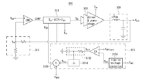
- FIG. 3 is a schematic circuit structure diagram of a constant frequency ON-time voltage regulator in accordance with an embodiment of the present invention.
- FIG. 3 is a schematic circuit structure diagram of a constant frequency ON-time voltage regulator in accordance with an embodiment of the present invention.
- the constant frequency ON-time voltage regulator 300 comprises a feedback circuit 311 , an error comparator CMP, a constant frequency ON-time control circuit 313 , a frequency setting parameter adjusting circuit 315 , a driver & power stage 330 and an output filter 350 ; herein, the error comparator CMP, the constant frequency ON-time control circuit 313 and the frequency setting parameter adjusting circuit 315 together construct a constant frequency ON-time control system of the embodiment.
- Duty i.e., the duty cycle of the pulse width modulation signal V PWM depicted in FIG. 1B
- the driver & power stage 330 is configured to determine a time length of an input voltage V IN inputted into the driver & power stage 330 according to an ON-time T ON outputted from the constant frequency ON-time control circuit 313 and thereby regulate the output voltage V OUT .
- the frequency setting parameter adjusting circuit 315 comprises a time-to-voltage convertor 3150 , an error amplifier EA, a low-pass filter 3152 , a polarity selection circuit 3154 and a computing circuit 3156 .
- the time-to-voltage convertor 3150 is configured to receive the OFF-time T OFF from the constant frequency ON-time control circuit 313 and convert the OFF-time T OFF into a control voltage V OFF which represents the OFF-time T OFF .
- the error amplifier EA is configured to receive the control voltage V OFF and a reference voltage V OFF(set) which represents an OFF-time reference value (herein, the OFF-time reference value is set to a value larger than the minimum OFF-time of the system), and output an error amplified signal S dif according to a difference between the control voltage V OFF and the reference voltage V OFF(set) .
- the error amplified signal S dif has a positive polarity (or S dif >0) if the control voltage V OFF is larger than the reference voltage V OFF(set) (or, the OFF-time T OFF is shorter than the OFF-time reference value correspondingly); otherwise, S dif ⁇ 0.
- the low-pass filter 3152 is configured to perform a low-pass filtering operation on the error amplified signal S dif and accordingly output a low-pass filtered error amplified signal S dif to the polarity selection circuit 3154 .
- the polarity selection circuit 3154 is configured to output the frequency setting parameter adjust value S con according to the low-pass filtered error amplified signal S dif .
- the frequency setting parameter adjust value S con is modulated to an non-zero value thereby the frequency setting parameter F SET is accordingly modulated for example to a smaller value when the OFF-time T OFF is smaller than the OFF-time reference value; alternatively, the frequency setting parameter adjust value S con is modulated to zero thereby the frequency setting parameter F SET is maintained at a preset value when the OFF-time T OFF is not smaller than the OFF-time reference value. Consequently, the problem of resulting in an over-low output voltage due to the minimum OFF-time limitation in the prior art is avoided in the embodiment of the present.
- the frequency setting parameter is modulated to a smaller value thereby the ON-time is modulated for example to a larger value when the OFF-time is shorter than the OFF-time reference value (the OFF-time reference value can be set to a value larger than the minimum OFF-time in a circuit implementation), consequently the problem of resulting in an over-low output voltage due to the minimum OFF-time limitation in the prior art is solved.
Landscapes
- Engineering & Computer Science (AREA)
- Power Engineering (AREA)
- Dc-Dc Converters (AREA)
Abstract
Description
- The present invention relates to a voltage regulator or a convertor, and more particularly to a constant frequency ON-time control system, a control method and a voltage regulator using the same.
-
FIG. 1A is a schematic circuit structure diagram of a conventional constant ON-time (COT) voltage regulator. As depicted inFIG. 1A , thevoltage regulator 100 comprises a feedback circuit 111, an error comparator CMP, an ON-time control circuit 113, a driver &power stage 130 and anoutput filter 150; herein, the error comparator CMP and the ON-time control circuit 113 together construct a constant ON-time control system. In thevoltage regulator 100, the error comparator CMP is configured to compare a reference voltage VREF to a feedback value VFB of an output voltage VOUT provided by the feedback circuit 111, and accordingly output an output voltage logic signal COMP based on the comparing result. The ON-time control circuit 113 is configured to generate and output an OFF-time and an ON-time TON according to a transition time of the voltage logic signal COMP. The driver &power stage 130 is configured to determine a time length of an input voltage VIN inputted to the driver &power stage 130 according to the received ON-time TON, thereby control an inductance current IL resulted in theoutput filter 150 so as to further modulate the output voltage VOUT.FIG. 1B is a schematic circuit diagram of apower stage part 1302 of the driver &power stage 130 depicted inFIG. 1A . As mentioned above, the driver &power stage 130 is configured to generate a pulse width modulation (PWM) signal VPWM (not shown) according to the ON-time TON thereby the ON-time and OFF-time (equal to the interval time length between two consecutive ON-time) of a transistor HS-MOS is accordingly determined by the pulse width modulation signal VPWM. Moreover, it is indicated that the two coupled transistors HS-MOS and LS-MOS are ON alternatively. - The conventional constant ON-time control system as depicted in
FIG. 1A has several advantages, such as having a simple circuit design, no need of a compensation circuit and having a quick response; however, the conventional constant ON-time control system also has disadvantages such as having a varying operation frequency manner. Today, many means are developed to make the constant ON-time control systems have a constant operation frequency manner.FIG. 2 is a schematic circuit structure diagram of a conventional constant frequency ON-time regulator 200. - As depicted in
FIG. 2 , the conventional constant frequency ON-time regulator 200 comprises a feedback circuit 211, an error comparator CMP, a constant frequency ON-time control circuit 213, a driver &power stage 230 and anoutput filter 250; herein, the error comparator CMP and the constant frequency ON-time control circuit 213 together construct a constant frequency ON-time control system. In the constant frequency ON-time regulator 200, the constant frequency ON-time control circuit 213 is configured to obtain a value (or an approximate value) of the system duty cycle Duty (i.e., the duty cycle of the pulse width modulation signal VPWM depicted inFIG. 1B ) of thevoltage regulator 200 according to the input voltage VIN and the output voltage VOUT, and accordingly output a corresponding ON-time TON (herein, TON=VOUT/(VIN×FSET0) or Duty×(1/FSET0) or Duty×(1/FSET0)) to the driver &power stage 230 based on a preset frequency setting parameter FSET0. Thereby, the operation frequency of the constant frequency ON-time regulator 200 is approximately modulated at a constant frequency which is corresponding to the preset frequency setting parameter FSET0. In addition, the OFF-time is automatically determined based on the error comparator CMP comparing the reference voltage VREF to the feedback value VFB of the output voltage VOUT. - However, in a practical circuit realization of a constant frequency ON-time regulator there is a limitation of the minimum OFF-time, which means the practical OFF-time cannot drop under a specific minimum OFF-time. Therefore, once the OFF-time, corresponding to the ON-time and generated by the constant frequency ON-
time control circuit 213 as depicted inFIG. 2 , is needed to be modulated shorter than the minimum OFF-time, the constant frequency ON-time control system will still maintain the OFF-time at a value of the minimum OFF-time, thereby the pulse width modulation signal VpPWM, composed by the minimum OFF-time and the ON-time TON generated by the constant frequency ON-time control circuit 213, may result in an over-low output voltage VOUT so as unable to maintain the output voltage VOUT at a preset level. - Therefore, an objective of the present invention is to provide a constant frequency ON-time control system for solving a problem of having an over-low output voltage resulted by the minimum OFF-time in the prior art.
- Another objective of the present invention is to provide a constant frequency ON-time control method for solving a problem of having an over-low output voltage resulted by the minimum OFF-time in the prior art.
- Still another objective of the present invention is to provide a voltage regulator applied to aforementioned constant frequency ON-time control system and the aforementioned constant frequency ON-time control method.
- One embodiment of the present invention discloses a constant frequency ON-time control system applied to a voltage regulator. The voltage regulator determines a time length of an input voltage inputted into the voltage regulator according to an ON-time and thereby regulating an output voltage. Specifically, the constant frequency ON-time control system comprises a constant frequency ON-time control circuit and a frequency setting parameter adjusting circuit. The constant frequency ON-time control circuit is for setting the ON-time according to a system duty cycle of the voltage regulator and a frequency setting parameter. The frequency setting parameter adjusting circuit is for generating a frequency setting parameter adjust value according to an OFF-time, which is corresponding to the ON-time and of the voltage regulator, and generating the frequency setting parameter through performing an operation on the frequency setting parameter adjust value and a preset frequency setting parameter. Herein, the frequency setting parameter adjusting circuit modulates the frequency setting parameter through changing a result of the operation based on the frequency setting parameter adjust value when the OFF-time is shorter than an OFF-time reference value, thereby increases the ON-time.
- In one embodiment, the above mentioned frequency setting parameter adjusting circuit comprises an error amplifier, a low-pass filter, a polarity selection circuit and a computing circuit. The error amplifier is for outputting an error amplified signal according to a difference between a control voltage representing the OFF-time and a reference voltage representing the OFF-time reference value, wherein the error amplified signal has a specific polarity when the OFF-time is shorter than the OFF-time reference value. The low-pass filter is for outputting a low-pass filtered error amplified signal through performing a low-pass filtering operation on the error amplified signal. The polarity selection circuit is for outputting the frequency setting parameter adjust value according to the low-pass filtered error amplified signal, and adjusting the frequency setting parameter adjust value to a non-zero value when the low-pass filtered error amplified signal is with the specific polarity. The computing circuit is for generating the frequency setting parameter through computing the preset frequency setting parameter and the frequency setting parameter adjust value, and providing the frequency setting parameter to the constant frequency ON-time control circuit.
- In one embodiment, the above mentioned frequency setting parameter adjusting circuit further comprises a time-to-voltage convertor for converting the OFF-time into the control voltage.
- In one embodiment, the above mentioned constant frequency ON-time control system further comprises an error comparator for generating an output voltage logic signal according to a feedback value of the output voltage and a reference voltage, and providing the output voltage logic signal to the constant frequency ON-time control circuit for determining the OFF-time.
- Another embodiment of the present invention discloses a constant frequency ON-time control method applied to a voltage regulator. The voltage regulator determines a time length of an input voltage inputted into the voltage regulator according to an ON-time and thereby regulating an output voltage. The constant frequency ON-time control method comprises steps of: setting the ON-time according to a system duty cycle of the voltage regulator and a frequency setting parameter; and changing the frequency setting parameter thereby increasing the ON-time when an OFF-time, corresponding to the ON-time and of the voltage regulator, is shorter than an OFF-time reference value.
- In one embodiment, the above mentioned step of changing the frequency setting parameter thereby increasing the ON-time when the OFF-time, corresponding to the ON-time and of the voltage regulator, is shorter than the OFF-time reference value comprises steps of: outputting an error amplified signal according to a difference between a control voltage representing the OFF-time and a reference voltage representing the OFF-time reference value, wherein the error amplified signal has a specific polarity when the OFF-time is shorter than the OFF-time reference value; outputting a low-pass filtered error amplified signal through performing a low-pass filtering operation on the error amplified signal; outputting a frequency setting parameter adjust value with an non-zero value when the low-pass filtered error amplified signal is with the specific polarity; and changing the frequency setting parameter through the frequency setting parameter adjust value with an non-zero value.
- In one embodiment, the above mentioned constant frequency ON-time control method further comprises steps of: providing an output voltage logic signal according to a difference between a feedback value of the output voltage and a reference voltage; and determining the OFF-time according to the output voltage logic signal.
- Another embodiment of the present invention discloses a voltage regulator. The voltage regulator comprises a driver & power stage, a constant frequency ON-time control circuit and a frequency setting parameter adjusting circuit. The driver & power stage is for determining a time length of an input voltage inputted into the driver & power stage according to an ON-time and thereby regulating an output voltage. The constant frequency ON-time control circuit is for setting the ON-time according to a system duty cycle of the voltage regulator and a frequency setting parameter. The frequency setting parameter adjusting circuit is for generating a frequency setting parameter adjust value according to an OFF-time which is corresponding to the ON-time, and determining whether to change the frequency setting parameter according to the frequency setting parameter adjust value. Wherein, the frequency setting parameter adjust value has a non-zero value thereby the frequency setting parameter is modulated when the OFF-time is shorter than an OFF-time reference value.
- In summary, through the frequency setting parameter adjusting circuit in the embodiment of the present invention, the frequency setting parameter is modulated to a smaller value thereby the ON-time is modulated for example to a larger value when the OFF-time is shorter than the OFF-time reference value (the OFF-time reference value can be set to a value larger than the minimum OFF-time in a circuit implementation), consequently the problem of resulting in decreasing output voltage due to the minimum OFF-time limitation in the prior art is solved.
- The above objects and advantages of the present invention will become more readily apparent to those ordinarily skilled in the art after reviewing the following detailed description and accompanying drawing, in which:
-
FIG. 1A is a schematic circuit structure diagram of a conventional constant ON-time (COT) voltage regulator; -
FIG. 1B is a schematic circuit diagram of a power stage part of the driver & power stage depicted inFIG. 1A ; -
FIG. 2 is a schematic circuit structure diagram of a conventional constant frequency ON-time regulator; and -
FIG. 3 is a schematic circuit structure diagram of a constant frequency ON-time voltage regulator in accordance with an embodiment of the present invention. - The present invention will now be described more specifically with reference to the following embodiments. It is to be noted that the following descriptions of preferred embodiments of this invention are presented herein for purpose of illustration and description only. It is not intended to be exhaustive or to be limited to the precise form disclosed.
-
FIG. 3 is a schematic circuit structure diagram of a constant frequency ON-time voltage regulator in accordance with an embodiment of the present invention. As depicted inFIG. 3 , the constant frequency ON-time voltage regulator 300 comprises afeedback circuit 311, an error comparator CMP, a constant frequency ON-time control circuit 313, a frequency settingparameter adjusting circuit 315, a driver &power stage 330 and anoutput filter 350; herein, the error comparator CMP, the constant frequency ON-time control circuit 313 and the frequency settingparameter adjusting circuit 315 together construct a constant frequency ON-time control system of the embodiment. - In the embodiment, basically the function of the
feedback circuit 311, error comparator CMP, driver &power stage 330 andoutput filter 350 is respectively same as that of the feedback circuit 111, error comparator CMP, driver &power stage 130 andoutput filter 150 depicted inFIGS. 1A and 2 ; thereby no any unnecessary detail is given here. - In the
voltage regulator 300 of the embodiment, the constant frequency ON-time control circuit 313 is configured to obtain a value (or an approximate value) of the system duty cycle Duty (i.e., the duty cycle of the pulse width modulation signal VPWM depicted inFIG. 1B ) of thevoltage regulator 300 according to the input voltage VIN and the output voltage VOUT; accordingly generate an ON-time TON based on the exemplary equation TON=VOUT/(VIN×FSET) or Duty×(1/FsET) or Duty×(1/FSET)), where FSET is the frequency setting parameter; and consequently determine an OFF-time, which is corresponding to the ON-time TON, according to an output voltage logic signal COMP outputted from the error comparator CMP through comparing the reference voltage VREF to the feedback value VFB of the output voltage VOUT. It is to be indicated that the system duty cycle Duty is not necessary to be obtained through dividing the output voltage VOUT by the input voltage VIN; the system duty cycle Duty can be obtained by other means. The driver &power stage 330 is configured to determine a time length of an input voltage VIN inputted into the driver &power stage 330 according to an ON-time TON outputted from the constant frequency ON-time control circuit 313 and thereby regulate the output voltage VOUT. - As depicted in
FIG. 3 , the frequency settingparameter adjusting circuit 315 comprises a time-to-voltage convertor 3150, an error amplifier EA, a low-pass filter 3152, apolarity selection circuit 3154 and acomputing circuit 3156. - In the frequency setting
parameter adjusting circuit 315 of the embodiment, the time-to-voltage convertor 3150 is configured to receive the OFF-time TOFF from the constant frequency ON-time control circuit 313 and convert the OFF-time TOFF into a control voltage VOFF which represents the OFF-time TOFF. The error amplifier EA is configured to receive the control voltage VOFF and a reference voltage VOFF(set) which represents an OFF-time reference value (herein, the OFF-time reference value is set to a value larger than the minimum OFF-time of the system), and output an error amplified signal Sdif according to a difference between the control voltage VOFF and the reference voltage VOFF(set). Specifically, the error amplified signal Sdif has a positive polarity (or Sdif>0) if the control voltage VOFF is larger than the reference voltage VOFF(set) (or, the OFF-time TOFF is shorter than the OFF-time reference value correspondingly); otherwise, Sdif≦0. The low-pass filter 3152 is configured to perform a low-pass filtering operation on the error amplified signal Sdif and accordingly output a low-pass filtered error amplified signal Sdif to thepolarity selection circuit 3154. Thepolarity selection circuit 3154 is configured to output the frequency setting parameter adjust value Scon according to the low-pass filtered error amplified signal Sdif. Specifically, thepolarity selection circuit 3154 sets the frequency setting parameter adjust value Scon to an non-zero value (or, Scon>0) when the error amplified signal Sdif>0; alternatively, thepolarity selection circuit 3154 sets the frequency setting parameter adjust value Scon to zero (or, Scon=0) when the error amplified signal Sdif≦0. Thecomputing circuit 3156 is configured to receive a preset frequency setting parameter FSET0 and the frequency setting parameter adjust value Scon, and perform an operation on the preset frequency setting parameter FSET0 and the frequency setting parameter adjust value Scon, thereby provide the result of the operation (or the frequency setting parameter FSET) to the constant frequency ON-time control circuit 313; herein, the operation is FSET=αFSET0−βScon, and the equation has a simplest form when α=β=1; however, it is noted that α and β can be set to other values. - Based on the equation of FSET=αFSET0−βScon in the embodiment, it is noted: the frequency setting parameter adjust value Scon is modulated to an non-zero value thereby the frequency setting parameter FSET is accordingly modulated for example to a smaller value when the OFF-time TOFF is smaller than the OFF-time reference value; alternatively, the frequency setting parameter adjust value Scon is modulated to zero thereby the frequency setting parameter FSET is maintained at a preset value when the OFF-time TOFF is not smaller than the OFF-time reference value. Consequently, the problem of resulting in an over-low output voltage due to the minimum OFF-time limitation in the prior art is avoided in the embodiment of the present.
- To sum up, through the frequency setting parameter adjusting circuit in the embodiment of the present invention, the frequency setting parameter is modulated to a smaller value thereby the ON-time is modulated for example to a larger value when the OFF-time is shorter than the OFF-time reference value (the OFF-time reference value can be set to a value larger than the minimum OFF-time in a circuit implementation), consequently the problem of resulting in an over-low output voltage due to the minimum OFF-time limitation in the prior art is solved.
- In addition, it is to be noted that as long as the purpose of modulating the frequency setting parameter to a smaller value is maintained when the OFF-time is shorter than the OFF-time reference value, the design of circuit structure of the voltage modulator, such as the frequency setting parameter adjusting circuit, in the embodiment can be properly modified by those ordinarily skilled in the art.
- While the invention has been described in terms of what is presently considered to be the most practical and preferred embodiments, it is to be understood that the invention needs not be limited to the disclosed embodiment. On the contrary, it is intended to cover various modifications and similar arrangements included within the spirit and scope of the appended claims which are to be accorded with the broadest interpretation so as to encompass all such modifications and similar structures.
Claims (12)
Applications Claiming Priority (3)
| Application Number | Priority Date | Filing Date | Title |
|---|---|---|---|
| TW100111622A TWI430069B (en) | 2011-04-01 | 2011-04-01 | Constant frequency on-time control system and method and voltage regulator using the same |
| TW100111622A | 2011-04-01 | ||
| TW100111622 | 2011-04-01 |
Publications (2)
| Publication Number | Publication Date |
|---|---|
| US20120249108A1 true US20120249108A1 (en) | 2012-10-04 |
| US8680831B2 US8680831B2 (en) | 2014-03-25 |
Family
ID=46926348
Family Applications (1)
| Application Number | Title | Priority Date | Filing Date |
|---|---|---|---|
| US13/181,686 Active 2032-02-21 US8680831B2 (en) | 2011-04-01 | 2011-07-13 | Constant frequency on-time control system and method and voltage regulator using the same |
Country Status (2)
| Country | Link |
|---|---|
| US (1) | US8680831B2 (en) |
| TW (1) | TWI430069B (en) |
Cited By (1)
| Publication number | Priority date | Publication date | Assignee | Title |
|---|---|---|---|---|
| CN114944748A (en) * | 2022-07-20 | 2022-08-26 | 中科(深圳)无线半导体有限公司 | Constant frequency control circuit and method for constant on-time control mode converter |
Families Citing this family (4)
| Publication number | Priority date | Publication date | Assignee | Title |
|---|---|---|---|---|
| TWI561118B (en) | 2014-08-13 | 2016-12-01 | Ind Tech Res Inst | Dimming system and operating method thereof |
| CN108011551B (en) * | 2017-12-24 | 2020-12-08 | 如东县燕川物业管理有限公司 | Differential modulation type constant frequency excitation generator voltage regulator with preset bidirectional narrow pulse |
| TWI699640B (en) * | 2019-05-16 | 2020-07-21 | 晶豪科技股份有限公司 | Contstant on-time controller and buck regulator device using the same |
| CN112994453B (en) | 2019-12-18 | 2025-02-11 | 力智电子股份有限公司 | Time signal generating circuit of power converter and control method thereof |
Citations (1)
| Publication number | Priority date | Publication date | Assignee | Title |
|---|---|---|---|---|
| US20080030181A1 (en) * | 2006-08-04 | 2008-02-07 | Kuo Ping Liu | Control circuit and method for a constant on-time PWM switching converter |
Family Cites Families (3)
| Publication number | Priority date | Publication date | Assignee | Title |
|---|---|---|---|---|
| US6476589B2 (en) | 2001-04-06 | 2002-11-05 | Linear Technology Corporation | Circuits and methods for synchronizing non-constant frequency switching regulators with a phase locked loop |
| TWI220329B (en) | 2003-07-22 | 2004-08-11 | Richtek Technology Corp | Device and method to improve noise sensitivity of switching system |
| US7304464B2 (en) | 2006-03-15 | 2007-12-04 | Micrel, Inc. | Switching voltage regulator with low current trickle mode |
-
2011
- 2011-04-01 TW TW100111622A patent/TWI430069B/en active
- 2011-07-13 US US13/181,686 patent/US8680831B2/en active Active
Patent Citations (1)
| Publication number | Priority date | Publication date | Assignee | Title |
|---|---|---|---|---|
| US20080030181A1 (en) * | 2006-08-04 | 2008-02-07 | Kuo Ping Liu | Control circuit and method for a constant on-time PWM switching converter |
Cited By (1)
| Publication number | Priority date | Publication date | Assignee | Title |
|---|---|---|---|---|
| CN114944748A (en) * | 2022-07-20 | 2022-08-26 | 中科(深圳)无线半导体有限公司 | Constant frequency control circuit and method for constant on-time control mode converter |
Also Published As
| Publication number | Publication date |
|---|---|
| TWI430069B (en) | 2014-03-11 |
| TW201241590A (en) | 2012-10-16 |
| US8680831B2 (en) | 2014-03-25 |
Similar Documents
| Publication | Publication Date | Title |
|---|---|---|
| US9154037B2 (en) | Current-mode buck converter and electronic system using the same | |
| US9621053B1 (en) | Peak power control technique for primary side controller operation in continuous conduction mode | |
| US10122278B1 (en) | Control circuit operating in pulse skip mode and voltage converter having the same | |
| US7952900B2 (en) | H-bridge buck-boost converter | |
| US8907646B2 (en) | Power converting circuit and feedback control circuit | |
| US8686701B2 (en) | Active wire compensation circuit and controller with the same | |
| US20140103993A1 (en) | Chip dynamic voltage regulator circuit and terminal device | |
| US9798348B2 (en) | Power converter dependent on a voltage range the input voltage resides in | |
| TWI511431B (en) | Dc/dc converter and method for controlling the same | |
| US20130043849A1 (en) | Voltage Converter Including Variable Mode Switching Regulator And Related Method | |
| US8680831B2 (en) | Constant frequency on-time control system and method and voltage regulator using the same | |
| US9866128B2 (en) | Semiconductor device and switching power supply device | |
| US9966849B1 (en) | Current mode voltage converter having fast transient response | |
| US10186965B2 (en) | Control circuit with hysteresis for a switching voltage regulator and related control method | |
| KR20130036065A (en) | Buck switch-mode power converter large signal transient response optimizer | |
| US10284070B2 (en) | Voltage conversion device and voltage conversion method | |
| US10003305B2 (en) | Apparatus and method for modulating supply for a power amplifier | |
| US6977830B2 (en) | Power supply apparatus | |
| JP2020156215A (en) | Switching power supply | |
| US7839126B2 (en) | Signal converting apparatus and signal conversion method providing adjusted error signal with modified swing range | |
| CN103023316A (en) | Dc-dc converter and dc-dc conversion method | |
| TW201904184A (en) | Dc-dc converting circuit and multi-phase power controller thereof | |
| US10135332B2 (en) | DC-DC converter | |
| US9035637B1 (en) | Systems and methods for controlling power converters | |
| US20060164056A1 (en) | Switching regulator control circuit and switching regulator |
Legal Events
| Date | Code | Title | Description |
|---|---|---|---|
| AS | Assignment |
Owner name: RICHTEK TECHNOLOGY CORP, TAIWAN Free format text: ASSIGNMENT OF ASSIGNORS INTEREST;ASSIGNORS:CHEN, AN-TUNG;TAI, TING-JUNG;REEL/FRAME:026583/0063 Effective date: 20110701 |
|
| FEPP | Fee payment procedure |
Free format text: PAYOR NUMBER ASSIGNED (ORIGINAL EVENT CODE: ASPN); ENTITY STATUS OF PATENT OWNER: LARGE ENTITY |
|
| STCF | Information on status: patent grant |
Free format text: PATENTED CASE |
|
| FEPP | Fee payment procedure |
Free format text: PAYER NUMBER DE-ASSIGNED (ORIGINAL EVENT CODE: RMPN); ENTITY STATUS OF PATENT OWNER: LARGE ENTITY Free format text: PAYOR NUMBER ASSIGNED (ORIGINAL EVENT CODE: ASPN); ENTITY STATUS OF PATENT OWNER: LARGE ENTITY |
|
| MAFP | Maintenance fee payment |
Free format text: PAYMENT OF MAINTENANCE FEE, 4TH YEAR, LARGE ENTITY (ORIGINAL EVENT CODE: M1551) Year of fee payment: 4 |
|
| MAFP | Maintenance fee payment |
Free format text: PAYMENT OF MAINTENANCE FEE, 8TH YEAR, LARGE ENTITY (ORIGINAL EVENT CODE: M1552); ENTITY STATUS OF PATENT OWNER: LARGE ENTITY Year of fee payment: 8 |
|
| MAFP | Maintenance fee payment |
Free format text: PAYMENT OF MAINTENANCE FEE, 12TH YEAR, LARGE ENTITY (ORIGINAL EVENT CODE: M1553); ENTITY STATUS OF PATENT OWNER: LARGE ENTITY Year of fee payment: 12 |