US20110240345A1 - Printed circuit board and method for making same - Google Patents
Printed circuit board and method for making same Download PDFInfo
- Publication number
- US20110240345A1 US20110240345A1 US12/764,963 US76496310A US2011240345A1 US 20110240345 A1 US20110240345 A1 US 20110240345A1 US 76496310 A US76496310 A US 76496310A US 2011240345 A1 US2011240345 A1 US 2011240345A1
- Authority
- US
- United States
- Prior art keywords
- pcb
- electrical element
- foils
- insulating layer
- copper foils
- Prior art date
- Legal status (The legal status is an assumption and is not a legal conclusion. Google has not performed a legal analysis and makes no representation as to the accuracy of the status listed.)
- Abandoned
Links
Images


Classifications
-
- H—ELECTRICITY
- H05—ELECTRIC TECHNIQUES NOT OTHERWISE PROVIDED FOR
- H05K—PRINTED CIRCUITS; CASINGS OR CONSTRUCTIONAL DETAILS OF ELECTRIC APPARATUS; MANUFACTURE OF ASSEMBLAGES OF ELECTRICAL COMPONENTS
- H05K1/00—Printed circuits
- H05K1/18—Printed circuits structurally associated with non-printed electric components
- H05K1/181—Printed circuits structurally associated with non-printed electric components associated with surface mounted components
-
- B—PERFORMING OPERATIONS; TRANSPORTING
- B32—LAYERED PRODUCTS
- B32B—LAYERED PRODUCTS, i.e. PRODUCTS BUILT-UP OF STRATA OF FLAT OR NON-FLAT, e.g. CELLULAR OR HONEYCOMB, FORM
- B32B37/00—Methods or apparatus for laminating, e.g. by curing or by ultrasonic bonding
- B32B37/02—Methods or apparatus for laminating, e.g. by curing or by ultrasonic bonding characterised by a sequence of laminating steps, e.g. by adding new layers at consecutive laminating stations
-
- B—PERFORMING OPERATIONS; TRANSPORTING
- B32—LAYERED PRODUCTS
- B32B—LAYERED PRODUCTS, i.e. PRODUCTS BUILT-UP OF STRATA OF FLAT OR NON-FLAT, e.g. CELLULAR OR HONEYCOMB, FORM
- B32B2311/00—Metals, their alloys or their compounds
-
- B—PERFORMING OPERATIONS; TRANSPORTING
- B32—LAYERED PRODUCTS
- B32B—LAYERED PRODUCTS, i.e. PRODUCTS BUILT-UP OF STRATA OF FLAT OR NON-FLAT, e.g. CELLULAR OR HONEYCOMB, FORM
- B32B2311/00—Metals, their alloys or their compounds
- B32B2311/16—Tin
-
- B—PERFORMING OPERATIONS; TRANSPORTING
- B32—LAYERED PRODUCTS
- B32B—LAYERED PRODUCTS, i.e. PRODUCTS BUILT-UP OF STRATA OF FLAT OR NON-FLAT, e.g. CELLULAR OR HONEYCOMB, FORM
- B32B2457/00—Electrical equipment
- B32B2457/08—PCBs, i.e. printed circuit boards
-
- H—ELECTRICITY
- H05—ELECTRIC TECHNIQUES NOT OTHERWISE PROVIDED FOR
- H05K—PRINTED CIRCUITS; CASINGS OR CONSTRUCTIONAL DETAILS OF ELECTRIC APPARATUS; MANUFACTURE OF ASSEMBLAGES OF ELECTRICAL COMPONENTS
- H05K2201/00—Indexing scheme relating to printed circuits covered by H05K1/00
- H05K2201/03—Conductive materials
- H05K2201/0332—Structure of the conductor
- H05K2201/0335—Layered conductors or foils
- H05K2201/0352—Differences between the conductors of different layers of a multilayer
-
- H—ELECTRICITY
- H05—ELECTRIC TECHNIQUES NOT OTHERWISE PROVIDED FOR
- H05K—PRINTED CIRCUITS; CASINGS OR CONSTRUCTIONAL DETAILS OF ELECTRIC APPARATUS; MANUFACTURE OF ASSEMBLAGES OF ELECTRICAL COMPONENTS
- H05K2201/00—Indexing scheme relating to printed circuits covered by H05K1/00
- H05K2201/09—Shape and layout
- H05K2201/09209—Shape and layout details of conductors
- H05K2201/09654—Shape and layout details of conductors covering at least two types of conductors provided for in H05K2201/09218 - H05K2201/095
- H05K2201/0979—Redundant conductors or connections, i.e. more than one current path between two points
-
- Y—GENERAL TAGGING OF NEW TECHNOLOGICAL DEVELOPMENTS; GENERAL TAGGING OF CROSS-SECTIONAL TECHNOLOGIES SPANNING OVER SEVERAL SECTIONS OF THE IPC; TECHNICAL SUBJECTS COVERED BY FORMER USPC CROSS-REFERENCE ART COLLECTIONS [XRACs] AND DIGESTS
- Y02—TECHNOLOGIES OR APPLICATIONS FOR MITIGATION OR ADAPTATION AGAINST CLIMATE CHANGE
- Y02P—CLIMATE CHANGE MITIGATION TECHNOLOGIES IN THE PRODUCTION OR PROCESSING OF GOODS
- Y02P70/00—Climate change mitigation technologies in the production process for final industrial or consumer products
- Y02P70/50—Manufacturing or production processes characterised by the final manufactured product
-
- Y—GENERAL TAGGING OF NEW TECHNOLOGICAL DEVELOPMENTS; GENERAL TAGGING OF CROSS-SECTIONAL TECHNOLOGIES SPANNING OVER SEVERAL SECTIONS OF THE IPC; TECHNICAL SUBJECTS COVERED BY FORMER USPC CROSS-REFERENCE ART COLLECTIONS [XRACs] AND DIGESTS
- Y10—TECHNICAL SUBJECTS COVERED BY FORMER USPC
- Y10T—TECHNICAL SUBJECTS COVERED BY FORMER US CLASSIFICATION
- Y10T156/00—Adhesive bonding and miscellaneous chemical manufacture
- Y10T156/10—Methods of surface bonding and/or assembly therefor
Definitions
- the present disclosure relates to a printed circuit board (PCB) and a method for making the same.
- PCB printed circuit board
- a central processing unit (CPU) and a power supply managing circuit are disposed on a printed circuit board (PCB) of a computer and connected to each other via a plurality of copper foils.
- a heat sink is disposed on the CPU for heat dissipation of the CPU.
- the volume of the heat sink is typically larger than the CPU. Therefore, it is necessary to leave a space between the CPU and the power supply managing circuit to position the heat sink.
- the copper foils are undesirably elongated, resulting in a larger resistance of the copper foils and accordingly a larger amount of power loss.
- FIG. 1 is a cross-sectional view of a printed circuit board (PCB) according to the disclosure.
- FIG. 2 is a circuit diagram of the PCB of FIG. 1 .
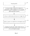
- FIG. 3 is a flow chart of a method of making the PCB of FIG. 1 .
- a printed circuit board (PCB) 1 is configured for connecting a first electrical element to a second electrical element.
- the first electrical element is a CPU 2 .
- the second electrical element is a power supply managing circuit 3 .
- the CPU 2 includes a plurality of input pins 21 .
- the power supply managing circuit 3 is electrically connected to a power supply (not shown) and configured for adjusting the voltage of the power supply to make the CPU 2 to work at a rated voltage and a rated current.
- the power supply managing circuit 3 includes a plurality of output pins 31 .
- the PCB 1 includes a base 10 , a plurality of copper foils 11 , an insulating layer 12 , and a plurality of metallic foils 13 .
- the insulating layer 12 is coated on the copper foils 11 .
- the metallic foils 13 such as tin foils, are coated on the insulating layer 12 .
- the copper foils 11 and the metallic foils 13 are used for connecting the output pins 31 of the power supply managing circuit 3 to the corresponding input pins 21 of the CPU 2 in parallel.
- the resistance of the copper foils 11 is represented as R 1 .
- the resistance of the metallic foils 13 is represented as R 2 .
- the copper foils 11 are parallelly and electrically connected to the metallic foils 13 .
- the method includes the following steps:
- S 2 Forming a plurality of copper foils 11 configured for connecting to a number of input pins 21 of a first electrical element 2 and a number of output pins 31 of a second electrical element 3 mounted on the PCB 1 .
- the first electrical element is a CPU
- the second electrical element is a power supply managing circuit.
- the insulating layer 12 is made of scaling powder.
- the metallic foils 13 are made of tin foil.
Landscapes
- Engineering & Computer Science (AREA)
- Microelectronics & Electronic Packaging (AREA)
- Printing Elements For Providing Electric Connections Between Printed Circuits (AREA)
- Structure Of Printed Boards (AREA)
Abstract
A printed circuit board (PCB) includes a base, copper foils, an insulating layer, and metallic foils. The copper foils are disposed on the base. The insulating layer is coated on the copper foils. The metallic foils are layered on the insulating layer. The copper foils and the metallic foils connect a first electrical element to a second electrical element.
Description
- 1. Technical Field
- The present disclosure relates to a printed circuit board (PCB) and a method for making the same.
- 2. Description of Related Art
- Generally, a central processing unit (CPU) and a power supply managing circuit are disposed on a printed circuit board (PCB) of a computer and connected to each other via a plurality of copper foils. A heat sink is disposed on the CPU for heat dissipation of the CPU. The volume of the heat sink is typically larger than the CPU. Therefore, it is necessary to leave a space between the CPU and the power supply managing circuit to position the heat sink. As a result, the copper foils are undesirably elongated, resulting in a larger resistance of the copper foils and accordingly a larger amount of power loss.
- Therefore, it is desirable to provide a PCB, which can overcome the above-discussed shortcomings.
- Many aspects of the embodiments should be better understood with reference to the following drawings. The components in the drawings are not necessarily drawn to scale, the emphasis instead being placed upon clearly illustrating the principles of the present disclosure. Moreover, in the drawings, like reference numerals designate corresponding parts throughout the several views.
-
FIG. 1 is a cross-sectional view of a printed circuit board (PCB) according to the disclosure. -
FIG. 2 is a circuit diagram of the PCB ofFIG. 1 . -
FIG. 3 is a flow chart of a method of making the PCB ofFIG. 1 . - Referring to
FIG. 1 , a printed circuit board (PCB) 1, according to a disclosure, is configured for connecting a first electrical element to a second electrical element. In the present disclosure, the first electrical element is aCPU 2. The second electrical element is a powersupply managing circuit 3. TheCPU 2 includes a plurality ofinput pins 21. The powersupply managing circuit 3 is electrically connected to a power supply (not shown) and configured for adjusting the voltage of the power supply to make theCPU 2 to work at a rated voltage and a rated current. The powersupply managing circuit 3 includes a plurality ofoutput pins 31. The PCB 1 includes abase 10, a plurality ofcopper foils 11, aninsulating layer 12, and a plurality ofmetallic foils 13. - The
insulating layer 12 is coated on thecopper foils 11. Themetallic foils 13, such as tin foils, are coated on theinsulating layer 12. Thecopper foils 11 and themetallic foils 13 are used for connecting theoutput pins 31 of the powersupply managing circuit 3 to thecorresponding input pins 21 of theCPU 2 in parallel. - Referring to
FIG. 2 , the resistance of thecopper foils 11 is represented as R1. The resistance of themetallic foils 13 is represented as R2. Thecopper foils 11 are parallelly and electrically connected to themetallic foils 13. As such, the total resistance of thecopper foils 11 and themetallic foils 13 is R=R1R2/(R1+R2). It is obvious that R will always be smaller than the R1. The power consumption of thecopper foils 11 and themetallic foils 13 is: P=I2R, where P is the power consumption and I is the rated current of theCPU 2. Obviously, power loss is reduced. - Referring to
FIG. 3 , a method of making the PCB is shown. The method includes the following steps: - S1: providing a
PCB 1. - S2: Forming a plurality of
copper foils 11 configured for connecting to a number ofinput pins 21 of a firstelectrical element 2 and a number ofoutput pins 31 of a secondelectrical element 3 mounted on thePCB 1. In the present disclosure, the first electrical element is a CPU, while the second electrical element is a power supply managing circuit. - S3: coating an
insulating layer 12 on the plurality ofcopper foils 11. In the present disclosure, theinsulating layer 12 is made of scaling powder. - S4: applying a plurality of
metallic foils 13 on theinsulating layer 12. - S5: connecting the
copper foils 11 and themetallic foils 13 to theinput pins 21 of the firstelectrical element 2 and theoutput pins 31 of the secondelectrical element 3. In the present disclosure, themetallic foils 13 are made of tin foil. - It will be understood that the above particular embodiments and methods are shown and described by way of illustration only. The principles and the features of the present disclosure may be employed in various and numerous embodiments thereof without departing from the scope of the disclosure as claimed. The above-described embodiments illustrate the scope of the disclosure but do not restrict the scope of the disclosure.
Claims (8)
1. A printed circuit board (PCB) comprising:
a base;
a plurality of copper foils disposed on the base;
an insulating layer coated on the copper foils;
a plurality of metallic foils coated on the insulating layer;
wherein the copper foils and the metallic foils are electrically connect a first electrical element and a second electrical element.
2. The PCB in claim 1 , wherein the metallic foils are made of tin foil.
3. The PCB in claim 2 , wherein the insulating layer is made of scaling powder.
4. The PCB in claim 1 , wherein the first electrical element is a CPU, and the second electrical element is a power supply managing circuit.
5. A method of making a PCB comprising the following:
providing a PCB;
forming a plurality of copper foils configured for connecting a first electrical element and a second electrical element mounted on the PCB;
coating an insulating layer on the plurality of copper foils;
applying a plurality of metallic foils on the insulating layer; and
connecting the copper foils and the metallic foils to the first electrical element and the second electrical element.
6. The method of making a PCB in claim 5 , wherein the metallic foils is made of tin foil.
7. The method of making a PCB in claim 6 , wherein the insulating layer is made of scaling powder.
8. The method of making a PCB in claim 5 , wherein the first electrical element is a CPU, while the second electrical element is a power supply managing circuit.
Applications Claiming Priority (2)
| Application Number | Priority Date | Filing Date | Title |
|---|---|---|---|
| TW99110228 | 2010-04-01 | ||
| TW099110228A TWI498058B (en) | 2010-04-01 | 2010-04-01 | Pcb and method for making same |
Publications (1)
| Publication Number | Publication Date |
|---|---|
| US20110240345A1 true US20110240345A1 (en) | 2011-10-06 |
Family
ID=44708293
Family Applications (1)
| Application Number | Title | Priority Date | Filing Date |
|---|---|---|---|
| US12/764,963 Abandoned US20110240345A1 (en) | 2010-04-01 | 2010-04-22 | Printed circuit board and method for making same |
Country Status (2)
| Country | Link |
|---|---|
| US (1) | US20110240345A1 (en) |
| TW (1) | TWI498058B (en) |
Citations (4)
| Publication number | Priority date | Publication date | Assignee | Title |
|---|---|---|---|---|
| US7180007B2 (en) * | 2003-06-06 | 2007-02-20 | Matsushita Electric Industrial Co., Ltd. | Electronic circuit device and its manufacturing method |
| US20080284007A1 (en) * | 2007-05-18 | 2008-11-20 | Fuji Electric Device Technology Co., Ltd. | Semiconductor module and method for manufacturing semiconductor module |
| US20090119914A1 (en) * | 2005-12-27 | 2009-05-14 | Clark Roger F | Process for Forming Electrical Contacts on a Semiconductor Wafer Using a Phase Changing Ink |
| US7675796B2 (en) * | 2005-12-27 | 2010-03-09 | Semiconductor Energy Laboratory Co., Ltd. | Semiconductor device |
Family Cites Families (2)
| Publication number | Priority date | Publication date | Assignee | Title |
|---|---|---|---|---|
| JP4207917B2 (en) * | 2005-04-01 | 2009-01-14 | セイコーエプソン株式会社 | Manufacturing method of multilayer substrate |
| TWI288556B (en) * | 2006-01-25 | 2007-10-11 | Arima Communication Corp | Communication product having impact-resistant structure and method for fabricating the same |
-
2010
- 2010-04-01 TW TW099110228A patent/TWI498058B/en not_active IP Right Cessation
- 2010-04-22 US US12/764,963 patent/US20110240345A1/en not_active Abandoned
Patent Citations (4)
| Publication number | Priority date | Publication date | Assignee | Title |
|---|---|---|---|---|
| US7180007B2 (en) * | 2003-06-06 | 2007-02-20 | Matsushita Electric Industrial Co., Ltd. | Electronic circuit device and its manufacturing method |
| US20090119914A1 (en) * | 2005-12-27 | 2009-05-14 | Clark Roger F | Process for Forming Electrical Contacts on a Semiconductor Wafer Using a Phase Changing Ink |
| US7675796B2 (en) * | 2005-12-27 | 2010-03-09 | Semiconductor Energy Laboratory Co., Ltd. | Semiconductor device |
| US20080284007A1 (en) * | 2007-05-18 | 2008-11-20 | Fuji Electric Device Technology Co., Ltd. | Semiconductor module and method for manufacturing semiconductor module |
Also Published As
| Publication number | Publication date |
|---|---|
| TW201136464A (en) | 2011-10-16 |
| TWI498058B (en) | 2015-08-21 |
Similar Documents
| Publication | Publication Date | Title |
|---|---|---|
| US9277640B2 (en) | Flexible printed circuit board and method for manufacturing same | |
| CN106410467B (en) | A processing technology of aluminum bus bar | |
| WO2014184102A3 (en) | Method for depositing thick copper layers onto sintered materials | |
| CN102625578A (en) | Light-emitting diode (LED) circuit board component | |
| KR20150021342A (en) | Multi Layered Printed Circuit Board | |
| US10709008B2 (en) | Power module assembly structure | |
| CN206422974U (en) | Bury planar resistor high-frequency multilayer wiring board | |
| US20110240345A1 (en) | Printed circuit board and method for making same | |
| US8625299B2 (en) | Circuit board with even current distribution | |
| CN203327376U (en) | Printed circuit board (PCB) for battery management system | |
| WO2015124036A1 (en) | Switching circuit structure based on printed circuit board | |
| US9905954B2 (en) | Power transmission device and manufacturing method thereof | |
| CN102215633A (en) | Circuit board and manufacturing method thereof | |
| CN105388411A (en) | A method for testing the current-carrying capacity of a circuit board | |
| CN103582291B (en) | A kind of metal base printed circuit board and electronic equipment | |
| CN203407071U (en) | Crimp blind hole circuit board | |
| CN202385400U (en) | Novel high-efficiency automatic-radiating PCB (printed circuit board) | |
| CN202269094U (en) | Printed circuit board modules and electronic equipment | |
| CN206323646U (en) | A kind of circuit board and electronic equipment | |
| EP3319407A1 (en) | Modular power supply | |
| CN205961558U (en) | Electrically conductive of paster and mobile terminal | |
| CN202353936U (en) | Light emitting diode (LED) circuit board module | |
| CN210899794U (en) | 3D cooling temperature control copper foil | |
| CN103929898A (en) | Method for manufacturing printed circuit board with ultra-thick copper layers | |
| CN207692157U (en) | A high-density PCB board with a stable interconnection structure |
Legal Events
| Date | Code | Title | Description |
|---|---|---|---|
| AS | Assignment |
Owner name: HON HAI PRECISION INDUSTRY CO., LTD., TAIWAN Free format text: ASSIGNMENT OF ASSIGNORS INTEREST;ASSIGNOR:SU, CHI-KUNG;REEL/FRAME:024268/0523 Effective date: 20100416 |
|
| STCB | Information on status: application discontinuation |
Free format text: ABANDONED -- FAILURE TO RESPOND TO AN OFFICE ACTION |