US20080098589A1 - Plated antenna from stamped metal coil - Google Patents
Plated antenna from stamped metal coil Download PDFInfo
- Publication number
- US20080098589A1 US20080098589A1 US11/775,974 US77597407A US2008098589A1 US 20080098589 A1 US20080098589 A1 US 20080098589A1 US 77597407 A US77597407 A US 77597407A US 2008098589 A1 US2008098589 A1 US 2008098589A1
- Authority
- US
- United States
- Prior art keywords
- recited
- plating
- antenna
- metal
- coil
- Prior art date
- Legal status (The legal status is an assumption and is not a legal conclusion. Google has not performed a legal analysis and makes no representation as to the accuracy of the status listed.)
- Granted
Links
Images


Classifications
-
- H—ELECTRICITY
- H01—ELECTRIC ELEMENTS
- H01Q—ANTENNAS, i.e. RADIO AERIALS
- H01Q1/00—Details of, or arrangements associated with, antennas
- H01Q1/36—Structural form of radiating elements, e.g. cone, spiral, umbrella; Particular materials used therewith
-
- B—PERFORMING OPERATIONS; TRANSPORTING
- B21—MECHANICAL METAL-WORKING WITHOUT ESSENTIALLY REMOVING MATERIAL; PUNCHING METAL
- B21D—WORKING OR PROCESSING OF SHEET METAL OR METAL TUBES, RODS OR PROFILES WITHOUT ESSENTIALLY REMOVING MATERIAL; PUNCHING METAL
- B21D28/00—Shaping by press-cutting; Perforating
- B21D28/02—Punching blanks or articles with or without obtaining scrap; Notching
- B21D28/10—Incompletely punching in such a manner that the parts are still coherent with the work
-
- Y—GENERAL TAGGING OF NEW TECHNOLOGICAL DEVELOPMENTS; GENERAL TAGGING OF CROSS-SECTIONAL TECHNOLOGIES SPANNING OVER SEVERAL SECTIONS OF THE IPC; TECHNICAL SUBJECTS COVERED BY FORMER USPC CROSS-REFERENCE ART COLLECTIONS [XRACs] AND DIGESTS
- Y10—TECHNICAL SUBJECTS COVERED BY FORMER USPC
- Y10T—TECHNICAL SUBJECTS COVERED BY FORMER US CLASSIFICATION
- Y10T29/00—Metal working
- Y10T29/49—Method of mechanical manufacture
- Y10T29/49002—Electrical device making
- Y10T29/49016—Antenna or wave energy "plumbing" making
- Y10T29/49018—Antenna or wave energy "plumbing" making with other electrical component
-
- Y—GENERAL TAGGING OF NEW TECHNOLOGICAL DEVELOPMENTS; GENERAL TAGGING OF CROSS-SECTIONAL TECHNOLOGIES SPANNING OVER SEVERAL SECTIONS OF THE IPC; TECHNICAL SUBJECTS COVERED BY FORMER USPC CROSS-REFERENCE ART COLLECTIONS [XRACs] AND DIGESTS
- Y10—TECHNICAL SUBJECTS COVERED BY FORMER USPC
- Y10T—TECHNICAL SUBJECTS COVERED BY FORMER US CLASSIFICATION
- Y10T29/00—Metal working
- Y10T29/49—Method of mechanical manufacture
- Y10T29/49002—Electrical device making
- Y10T29/4902—Electromagnet, transformer or inductor
- Y10T29/49071—Electromagnet, transformer or inductor by winding or coiling
-
- Y—GENERAL TAGGING OF NEW TECHNOLOGICAL DEVELOPMENTS; GENERAL TAGGING OF CROSS-SECTIONAL TECHNOLOGIES SPANNING OVER SEVERAL SECTIONS OF THE IPC; TECHNICAL SUBJECTS COVERED BY FORMER USPC CROSS-REFERENCE ART COLLECTIONS [XRACs] AND DIGESTS
- Y10—TECHNICAL SUBJECTS COVERED BY FORMER USPC
- Y10T—TECHNICAL SUBJECTS COVERED BY FORMER US CLASSIFICATION
- Y10T29/00—Metal working
- Y10T29/49—Method of mechanical manufacture
- Y10T29/49002—Electrical device making
- Y10T29/4902—Electromagnet, transformer or inductor
- Y10T29/49073—Electromagnet, transformer or inductor by assembling coil and core
-
- Y—GENERAL TAGGING OF NEW TECHNOLOGICAL DEVELOPMENTS; GENERAL TAGGING OF CROSS-SECTIONAL TECHNOLOGIES SPANNING OVER SEVERAL SECTIONS OF THE IPC; TECHNICAL SUBJECTS COVERED BY FORMER USPC CROSS-REFERENCE ART COLLECTIONS [XRACs] AND DIGESTS
- Y10—TECHNICAL SUBJECTS COVERED BY FORMER USPC
- Y10T—TECHNICAL SUBJECTS COVERED BY FORMER US CLASSIFICATION
- Y10T29/00—Metal working
- Y10T29/49—Method of mechanical manufacture
- Y10T29/49002—Electrical device making
- Y10T29/49117—Conductor or circuit manufacturing
Definitions
- This invention generally relates to RF antennas. More particularly, this invention relates to a method of fabricating a plated RF antenna.
- Transmitting devices such as a transmitter and a receiver for a remote keyless entry system require a radio frequency (RF) antenna.
- the RF antenna is typically fabricated from copper that is then plated with tin to facilitate soldering to a circuit assembly.
- Conventional RF antennas are delicate parts with long thin parts that must be handled with great care, and therefore at an increased cost.
- the plating material is applied after the RF antenna is stamped so that all surfaces can be thoroughly coated with plating.
- the stamped parts are fragile and require deliberate and careful handling that consumes an undesirable amount of time.
- An example method for fabricating an antenna for mounting onto a circuit board includes the initial step of stamping an unplated coil of metal strip with a plurality of initial openings that define portions of the RF antenna, plating the metal strip with the initial openings and finish stamping the final shape of the RF antenna to provide the completed part configuration.
- the example stamping operation includes stamping initial openings and re-rolling the initially stamped metal strip into a coil.
- the metal coil with initial stamped openings is then plated in one process.
- the plating process includes depositing plating material on the exposed surfaces of the coil. Because the initial openings provide additional exposed surfaces in the plated metal strip, interior sides of those openings are also plated.
- a final stamping process is formed that completes the RF antenna.
- the opening and final cuts performed during final stamping correspond to the openings created during the initial stamping process to form the completed plated shape.
- FIG. 1 is a schematic illustration of an initial step of the example method.
- FIG. 2 is a schematic illustration of a plating of a metal coil.
- FIG. 3 is a side view of the initial opening stamped into the metal coil.
- FIG. 4 is another side view of the initially stamped metal strip.
- FIG. 5 is a schematic illustration of the final stamping process.
- FIG. 6 is a schematic illustration of a portion of a completed RF antenna.
- FIG. 7 is a perspective view of an example completed RF antenna.
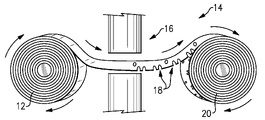
- the example process begins with an initial stamping process indicated at 14 .
- a bare coil of metal strip 12 is unrolled and stamped by a stamping press 16 .
- the stamping press 16 creates initial openings 18 within the metal coil 12 .
- the metal coil 12 is then re-rolled into an initially stamped coil 20 .
- the initial openings 18 provide a portion of the features of the completed RF antenna by defining specific areas of the RF antenna to which plating is required on all surfaces.
- the coil 12 of metal strip comprises a top surface, a bottom surface and two side surfaces.
- the top surface, the bottom surface and the side surfaces are plated.
- additional stamping processes after plating result in some unplated surfaces. Therefore, conventional processes perform all the stamping operations prior to any plating steps.
- Mounting of the RF antenna to a circuit board includes a soldering process that requires tin plating to be equally distributed on specific portions of the RF antenna.
- the tin plating is required to provide a desired soldered joint between the RF antenna and the circuit board.
- Conventional processes for stamping and fabricating the RF antenna include a complete stamping of the RF antenna followed by plating of the completed part.
- the RF antenna includes delicate fragile features that are susceptible to damage during plating and the handling that accompanies the plating process.
- the example method and process includes initial stamping of the openings 18 to define portions of the RF antenna that require plating on all sides.
- the metal strip is not detached from the coil 12 but is recoiled as an initially stamped coil 20 which is in turn plated as a complete continuous metal strip.
- the plating material is therefore deposited on the top bottom and all side surfaces that are defined by the initial openings 18 .
- the entire re-rolled initially stamped metal coil 20 is plated as one single unit. Plating of the entire coil 22 of metal strip material as one complete unit eases handling concerns during this process and provides a more uniform thickness for the plating material being deposited on all surfaces of the metal strip.
- the initially stamped metal strip includes features 40 that define portions of pins and other connecting elements of the RF antenna.
- the example initial openings 18 are created in the metal strip on each side of the connecting pins 40 .
- the example initial openings 18 define portions of the connecting pins 40 , but other features that require plating on all sides in the completed part could also be initially formed to accept plating on all sides prior to a complete stamped part.
- the connecting pins 40 are plated on a top surface 44 , a bottom surface 46 and each of side surfaces 48 to produce the desired complete plating of the part.
- the initial openings 18 provide for deposit of plating material 24 to the side surfaces 48 that are adjacent the connecting pins 40 .
- the initial openings 18 thereby generate the desired transverse surfaces that accept plating on each side 48 of the connecting pins 40 .
- the top surface 44 and bottom surface 46 are plated along with the side surfaces 48 that are defined by the initial openings 18 .
- the plating material 24 is deposited at a consistent uniform thickness on all exposed surfaces of the metal strip. This uniform deposit of plating material is carried through the transverse side surfaces 48 created by the initial openings 18 .
- the plated coil 26 is then moved to a final stamping step for shaping the RF antenna 15 that is accomplished by utilizing the plated coil 26 with the initial openings 18 .
- a final stamping press 32 completes the configuration of the RF antenna 15 by removing the remainder of material required to form the desired shape of the RF antenna. Because the initial openings 18 are already formed, the final stamping process removes material in portions where the plating material 24 is not required.
- the final stamping process 30 cuts the metal strip and results in some portions comprising bare unplated metal sides 80 . However, because the initial openings 18 were previously cut and plated, these plated portions remain intact.
- the RF antenna 15 is cut by the final stamping press 32 .
- the final cutting process performed does not re-cut the initial openings 18 , but performs cuts that correspond to the initial openings 18 .
- Plated sides 52 of the pins remain intact, while other surfaces that are cut in the final stamping process comprise the bare unplated metal surfaces 50 .
- the unplated surfaces 50 are not joint locations and therefore do not require the full plating that is required at each of the connecting pins 40 .
- the example RF antenna 15 includes the plated connecting pins 40 .
- the desired shape of these connecting pins 40 is initially defined at the initial stamping step 14 by the initial openings 18 .
- the final stamping of the RF antenna 15 includes other features that may join the initial openings 18 , but does not recut the initial openings 18 . Therefore, the connecting pins 40 remain coated with the plating material 24 to the thickness that is desired to accomplish the soldering or create the joint with the circuit board.
- the example RF antenna 15 includes the connector pins 40 that include the plated surface 52 on the top, bottom and both sides. Other portions of the connector of the RF antenna 15 that were stamped and cut at the final stamping step 30 include plating on the top side, the bottom side and bare metal 50 on each of the first and second sides.
- the initial openings 18 defining the pins 40 expose the side so that plating can be deposited on the metal strip prior to final formation of the delicate features of the RF antenna 15 .
- plating material can be applied prior to complete formation of the completed part 15 .
- the plated coil with defined initial openings 18 provides for a final stamping process that generates a completed and plated part. No additional processes are required once the final stamping process is completed.
Landscapes
- Engineering & Computer Science (AREA)
- Mechanical Engineering (AREA)
- Details Of Aerials (AREA)
Abstract
Description
- The application claims priority to U.S. Provisional Application No. 60/854,252 which was filed on Oct. 25, 2006.
- This invention generally relates to RF antennas. More particularly, this invention relates to a method of fabricating a plated RF antenna.
- Transmitting devices such as a transmitter and a receiver for a remote keyless entry system require a radio frequency (RF) antenna. The RF antenna is typically fabricated from copper that is then plated with tin to facilitate soldering to a circuit assembly. Conventional RF antennas are delicate parts with long thin parts that must be handled with great care, and therefore at an increased cost. The plating material is applied after the RF antenna is stamped so that all surfaces can be thoroughly coated with plating. The stamped parts are fragile and require deliberate and careful handling that consumes an undesirable amount of time.
- Accordingly, it is desirable to develop and design a process for plating parts that limits required handling of delicately featured parts.
- An example method for fabricating an antenna for mounting onto a circuit board includes the initial step of stamping an unplated coil of metal strip with a plurality of initial openings that define portions of the RF antenna, plating the metal strip with the initial openings and finish stamping the final shape of the RF antenna to provide the completed part configuration.
- The example stamping operation includes stamping initial openings and re-rolling the initially stamped metal strip into a coil. The metal coil with initial stamped openings is then plated in one process. The plating process includes depositing plating material on the exposed surfaces of the coil. Because the initial openings provide additional exposed surfaces in the plated metal strip, interior sides of those openings are also plated.
- Once the metal coil has been plated, a final stamping process is formed that completes the RF antenna. The opening and final cuts performed during final stamping correspond to the openings created during the initial stamping process to form the completed plated shape.
- These and other features of the present invention can be best understood from the following specification and drawings, the following of which is a brief description.
-
FIG. 1 is a schematic illustration of an initial step of the example method. -
FIG. 2 is a schematic illustration of a plating of a metal coil. -
FIG. 3 is a side view of the initial opening stamped into the metal coil. -
FIG. 4 is another side view of the initially stamped metal strip. -
FIG. 5 is a schematic illustration of the final stamping process. -
FIG. 6 is a schematic illustration of a portion of a completed RF antenna. -
FIG. 7 is a perspective view of an example completed RF antenna. - Referring to
FIG. 1 , the example process begins with an initial stamping process indicated at 14. During the initial stamping process 14 a bare coil ofmetal strip 12 is unrolled and stamped by a stampingpress 16. Thestamping press 16 createsinitial openings 18 within themetal coil 12. Themetal coil 12 is then re-rolled into an initially stampedcoil 20. Theinitial openings 18 provide a portion of the features of the completed RF antenna by defining specific areas of the RF antenna to which plating is required on all surfaces. - The
coil 12 of metal strip comprises a top surface, a bottom surface and two side surfaces. In normal plating operations the top surface, the bottom surface and the side surfaces are plated. However, additional stamping processes after plating result in some unplated surfaces. Therefore, conventional processes perform all the stamping operations prior to any plating steps. - Mounting of the RF antenna to a circuit board includes a soldering process that requires tin plating to be equally distributed on specific portions of the RF antenna. The tin plating is required to provide a desired soldered joint between the RF antenna and the circuit board. Conventional processes for stamping and fabricating the RF antenna include a complete stamping of the RF antenna followed by plating of the completed part. The RF antenna includes delicate fragile features that are susceptible to damage during plating and the handling that accompanies the plating process.
- The example method and process includes initial stamping of the
openings 18 to define portions of the RF antenna that require plating on all sides. The metal strip is not detached from thecoil 12 but is recoiled as an initially stampedcoil 20 which is in turn plated as a complete continuous metal strip. The plating material is therefore deposited on the top bottom and all side surfaces that are defined by theinitial openings 18. - Referring to
FIG. 2 , the entire re-rolled initially stampedmetal coil 20 is plated as one single unit. Plating of theentire coil 22 of metal strip material as one complete unit eases handling concerns during this process and provides a more uniform thickness for the plating material being deposited on all surfaces of the metal strip. - Referring to
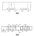
FIG. 3 , the initially stamped metal strip includesfeatures 40 that define portions of pins and other connecting elements of the RF antenna. The exampleinitial openings 18 are created in the metal strip on each side of the connectingpins 40. The exampleinitial openings 18 define portions of the connectingpins 40, but other features that require plating on all sides in the completed part could also be initially formed to accept plating on all sides prior to a complete stamped part. - Referring to
FIG. 4 , during the plating process, the connectingpins 40 are plated on a top surface 44, abottom surface 46 and each ofside surfaces 48 to produce the desired complete plating of the part. Theinitial openings 18 provide for deposit of platingmaterial 24 to theside surfaces 48 that are adjacent the connectingpins 40. Theinitial openings 18 thereby generate the desired transverse surfaces that accept plating on eachside 48 of the connectingpins 40. - During plating, the top surface 44 and
bottom surface 46 are plated along with theside surfaces 48 that are defined by theinitial openings 18. The platingmaterial 24 is deposited at a consistent uniform thickness on all exposed surfaces of the metal strip. This uniform deposit of plating material is carried through thetransverse side surfaces 48 created by theinitial openings 18. - Referring to
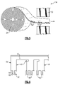
FIGS. 5 and 6 , theplated coil 26 is then moved to a final stamping step for shaping theRF antenna 15 that is accomplished by utilizing theplated coil 26 with theinitial openings 18. Afinal stamping press 32 completes the configuration of theRF antenna 15 by removing the remainder of material required to form the desired shape of the RF antenna. Because theinitial openings 18 are already formed, the final stamping process removes material in portions where the platingmaterial 24 is not required. Thefinal stamping process 30 cuts the metal strip and results in some portions comprising bare unplated metal sides 80. However, because theinitial openings 18 were previously cut and plated, these plated portions remain intact. - The
RF antenna 15 is cut by thefinal stamping press 32. The final cutting process performed does not re-cut theinitial openings 18, but performs cuts that correspond to theinitial openings 18. Platedsides 52 of the pins remain intact, while other surfaces that are cut in the final stamping process comprise the bareunplated metal surfaces 50. Theunplated surfaces 50 are not joint locations and therefore do not require the full plating that is required at each of the connectingpins 40. - Referring to
FIG. 6 , theexample RF antenna 15 includes the plated connecting pins 40. The desired shape of these connectingpins 40 is initially defined at theinitial stamping step 14 by theinitial openings 18. The final stamping of theRF antenna 15 includes other features that may join theinitial openings 18, but does not recut theinitial openings 18. Therefore, the connectingpins 40 remain coated with the platingmaterial 24 to the thickness that is desired to accomplish the soldering or create the joint with the circuit board. - Referring to
FIG. 7 , theexample RF antenna 15 includes the connector pins 40 that include the platedsurface 52 on the top, bottom and both sides. Other portions of the connector of theRF antenna 15 that were stamped and cut at thefinal stamping step 30 include plating on the top side, the bottom side andbare metal 50 on each of the first and second sides. Theinitial openings 18 defining thepins 40 expose the side so that plating can be deposited on the metal strip prior to final formation of the delicate features of theRF antenna 15. - Because of the initial stamping process defines surfaces of the completed
RF antenna 15 that require plating, plating material can be applied prior to complete formation of the completedpart 15. The plated coil with definedinitial openings 18 provides for a final stamping process that generates a completed and plated part. No additional processes are required once the final stamping process is completed. - Although a preferred embodiment of this invention has been disclosed, a worker of ordinary skill in this art would recognize that certain modifications would come within the scope of this invention. For that reason, the following claims should be studied to determine the true scope and content of this invention.
Claims (15)
Priority Applications (1)
| Application Number | Priority Date | Filing Date | Title |
|---|---|---|---|
| US11/775,974 US7637000B2 (en) | 2006-10-25 | 2007-07-11 | Plated antenna from stamped metal coil |
Applications Claiming Priority (2)
| Application Number | Priority Date | Filing Date | Title |
|---|---|---|---|
| US85425206P | 2006-10-25 | 2006-10-25 | |
| US11/775,974 US7637000B2 (en) | 2006-10-25 | 2007-07-11 | Plated antenna from stamped metal coil |
Publications (2)
| Publication Number | Publication Date |
|---|---|
| US20080098589A1 true US20080098589A1 (en) | 2008-05-01 |
| US7637000B2 US7637000B2 (en) | 2009-12-29 |
Family
ID=38646553
Family Applications (1)
| Application Number | Title | Priority Date | Filing Date |
|---|---|---|---|
| US11/775,974 Expired - Fee Related US7637000B2 (en) | 2006-10-25 | 2007-07-11 | Plated antenna from stamped metal coil |
Country Status (2)
| Country | Link |
|---|---|
| US (1) | US7637000B2 (en) |
| WO (1) | WO2008051641A1 (en) |
Cited By (2)
| Publication number | Priority date | Publication date | Assignee | Title |
|---|---|---|---|---|
| US20120193801A1 (en) * | 2011-01-27 | 2012-08-02 | Texas Instruments Deutschland Gmbh | Rfid transponder and method for connecting a semiconductor die to an antenna |
| WO2023091876A1 (en) * | 2021-11-19 | 2023-05-25 | Commscope Technologies Llc | Base station antennas including feed circuitry and calibration circuitry that share a board |
Families Citing this family (1)
| Publication number | Priority date | Publication date | Assignee | Title |
|---|---|---|---|---|
| US9252478B2 (en) | 2013-03-15 | 2016-02-02 | A.K. Stamping Company, Inc. | Method of manufacturing stamped antenna |
Citations (7)
| Publication number | Priority date | Publication date | Assignee | Title |
|---|---|---|---|---|
| US5199157A (en) * | 1992-01-21 | 1993-04-06 | Adaptive Technology, Inc. | Continuous manufacture of formed, plated component parts having selected alternate configurations |
| US5862579A (en) * | 1994-10-14 | 1999-01-26 | Press Engineering (Proprietary) Company | File fastener method of manufacture |
| US6326920B1 (en) * | 2000-03-09 | 2001-12-04 | Avaya Technology Corp. | Sheet-metal antenna |
| US6917333B2 (en) * | 2001-11-09 | 2005-07-12 | Hitachi Cable Ltd. | Flat-plate antenna and method for manufacturing the same |
| US7237319B2 (en) * | 2003-05-14 | 2007-07-03 | Shinko Electric Industries Co., Ltd. | Method of manufacturing a plane coil |
| US7256738B2 (en) * | 1998-02-27 | 2007-08-14 | Kabushiki Kaisha Miyake | Resonant circuits |
| US20070229360A1 (en) * | 2006-03-30 | 2007-10-04 | Fujitsu Component Limited | Antenna apparatus and manufacturing method thereof |
Family Cites Families (3)
| Publication number | Priority date | Publication date | Assignee | Title |
|---|---|---|---|---|
| DE2305874A1 (en) | 1973-02-07 | 1974-08-08 | Gottfried Rettich | Plastics coated stamping prodn. - by stamping presses with spray unit and central pulse control unit |
| DE10154217C1 (en) | 2001-11-07 | 2002-10-24 | Thyssenkrupp Stahl Ag | Surface finishing system for workpieces continuously stamped out of band of metallic foil has cutter station followed by finishing station, after which workpieces are separated from band |
| JP2003218620A (en) | 2002-01-24 | 2003-07-31 | Hitachi Cable Ltd | Method for manufacturing flat antenna |
-
2007
- 2007-07-11 US US11/775,974 patent/US7637000B2/en not_active Expired - Fee Related
- 2007-07-23 WO PCT/US2007/074068 patent/WO2008051641A1/en not_active Ceased
Patent Citations (7)
| Publication number | Priority date | Publication date | Assignee | Title |
|---|---|---|---|---|
| US5199157A (en) * | 1992-01-21 | 1993-04-06 | Adaptive Technology, Inc. | Continuous manufacture of formed, plated component parts having selected alternate configurations |
| US5862579A (en) * | 1994-10-14 | 1999-01-26 | Press Engineering (Proprietary) Company | File fastener method of manufacture |
| US7256738B2 (en) * | 1998-02-27 | 2007-08-14 | Kabushiki Kaisha Miyake | Resonant circuits |
| US6326920B1 (en) * | 2000-03-09 | 2001-12-04 | Avaya Technology Corp. | Sheet-metal antenna |
| US6917333B2 (en) * | 2001-11-09 | 2005-07-12 | Hitachi Cable Ltd. | Flat-plate antenna and method for manufacturing the same |
| US7237319B2 (en) * | 2003-05-14 | 2007-07-03 | Shinko Electric Industries Co., Ltd. | Method of manufacturing a plane coil |
| US20070229360A1 (en) * | 2006-03-30 | 2007-10-04 | Fujitsu Component Limited | Antenna apparatus and manufacturing method thereof |
Cited By (2)
| Publication number | Priority date | Publication date | Assignee | Title |
|---|---|---|---|---|
| US20120193801A1 (en) * | 2011-01-27 | 2012-08-02 | Texas Instruments Deutschland Gmbh | Rfid transponder and method for connecting a semiconductor die to an antenna |
| WO2023091876A1 (en) * | 2021-11-19 | 2023-05-25 | Commscope Technologies Llc | Base station antennas including feed circuitry and calibration circuitry that share a board |
Also Published As
| Publication number | Publication date |
|---|---|
| US7637000B2 (en) | 2009-12-29 |
| WO2008051641A1 (en) | 2008-05-02 |
Similar Documents
| Publication | Publication Date | Title |
|---|---|---|
| US7928919B2 (en) | Microwave antenna and method for making same | |
| US5045973A (en) | Procedure for manufacturing a radio telephone chassis and a chassis manufactured according to this procedure | |
| US7183498B2 (en) | High-frequency module and electronic device using the module | |
| JPH0799137A (en) | Three-terminal type noise filter and manufacture thereof | |
| EP2092593B1 (en) | Radio frequency filter | |
| DE10016037A1 (en) | Method for producing a label or a chip card, device for carrying out the method and a label or chip card produced thereafter | |
| US7637000B2 (en) | Plated antenna from stamped metal coil | |
| US6442990B1 (en) | Method of manufacturing a plate-shaped member having a recess and press die for forming recesses | |
| US7284320B2 (en) | Multilayer printed wiring board and method of manufacturing the same | |
| JP2003086037A (en) | Manufacturing method of terminalized electric wire, terminalized electric wire and electric connection box | |
| JPH09102342A (en) | Face mounting type coaxial connector and manufacture thereof | |
| US20080010809A1 (en) | Method of manufacturing a sticker type antenna | |
| US5639014A (en) | Integral solder and plated sealing cover and method of making same | |
| JP3994282B2 (en) | Manufacturing method for male terminal fittings | |
| US20020149460A1 (en) | Pin set of transformer coil and method for manufacturing the same | |
| EP0739675B1 (en) | Liquid crystal display panel holding metal fixture | |
| US7235742B2 (en) | Circuit board connector | |
| US20080211605A1 (en) | Coupling Lines For a Yig Filter or Yig Oscillator and Method For Producing the Coupling Lines | |
| JPH10247819A (en) | Antenna element and manufacture therefor | |
| JP2798478B2 (en) | Connection conductor and method of manufacturing the same | |
| JPH03286512A (en) | Manufacture of inductor contained in case | |
| JPH07111114A (en) | Method for manufacturing shielded tape electric wire | |
| JPH10201186A (en) | Manufacturing method of punching type coil | |
| CN120545662A (en) | Antenna module and manufacturing method thereof | |
| JPH0722818A (en) | Input/output terminal working method for antenna multicoupler |
Legal Events
| Date | Code | Title | Description |
|---|---|---|---|
| AS | Assignment |
Owner name: SIEMENS VDO AUTOMOTIVE CORPORATION, MICHIGAN Free format text: ASSIGNMENT OF ASSIGNORS INTEREST;ASSIGNOR:CLARK, JEFFREY A.;REEL/FRAME:019542/0061 Effective date: 20070702 |
|
| FEPP | Fee payment procedure |
Free format text: PAYOR NUMBER ASSIGNED (ORIGINAL EVENT CODE: ASPN); ENTITY STATUS OF PATENT OWNER: LARGE ENTITY Free format text: PAYER NUMBER DE-ASSIGNED (ORIGINAL EVENT CODE: RMPN); ENTITY STATUS OF PATENT OWNER: LARGE ENTITY |
|
| FPAY | Fee payment |
Year of fee payment: 4 |
|
| REMI | Maintenance fee reminder mailed | ||
| LAPS | Lapse for failure to pay maintenance fees |
Free format text: PATENT EXPIRED FOR FAILURE TO PAY MAINTENANCE FEES (ORIGINAL EVENT CODE: EXP.) |
|
| STCH | Information on status: patent discontinuation |
Free format text: PATENT EXPIRED DUE TO NONPAYMENT OF MAINTENANCE FEES UNDER 37 CFR 1.362 |
|
| FP | Lapsed due to failure to pay maintenance fee |
Effective date: 20171229 |