US20080098270A1 - Method For Determining Time to Failure of Submicron Metal Interconnects - Google Patents
Method For Determining Time to Failure of Submicron Metal Interconnects Download PDFInfo
- Publication number
- US20080098270A1 US20080098270A1 US11/596,264 US59626405A US2008098270A1 US 20080098270 A1 US20080098270 A1 US 20080098270A1 US 59626405 A US59626405 A US 59626405A US 2008098270 A1 US2008098270 A1 US 2008098270A1
- Authority
- US
- United States
- Prior art keywords
- time
- failure
- interconnects
- test
- interconnect
- Prior art date
- Legal status (The legal status is an assumption and is not a legal conclusion. Google has not performed a legal analysis and makes no representation as to the accuracy of the status listed.)
- Granted
Links
Images


Classifications
-
- G—PHYSICS
- G01—MEASURING; TESTING
- G01R—MEASURING ELECTRIC VARIABLES; MEASURING MAGNETIC VARIABLES
- G01R31/00—Arrangements for testing electric properties; Arrangements for locating electric faults; Arrangements for electrical testing characterised by what is being tested not provided for elsewhere
- G01R31/28—Testing of electronic circuits, e.g. by signal tracer
- G01R31/2851—Testing of integrated circuits [IC]
- G01R31/2884—Testing of integrated circuits [IC] using dedicated test connectors, test elements or test circuits on the IC under test
-
- G—PHYSICS
- G01—MEASURING; TESTING
- G01R—MEASURING ELECTRIC VARIABLES; MEASURING MAGNETIC VARIABLES
- G01R31/00—Arrangements for testing electric properties; Arrangements for locating electric faults; Arrangements for electrical testing characterised by what is being tested not provided for elsewhere
- G01R31/28—Testing of electronic circuits, e.g. by signal tracer
- G01R31/2851—Testing of integrated circuits [IC]
- G01R31/2855—Environmental, reliability or burn-in testing
- G01R31/2856—Internal circuit aspects, e.g. built-in test features; Test chips; Measuring material aspects, e.g. electro migration [EM]
- G01R31/2858—Measuring of material aspects, e.g. electro-migration [EM], hot carrier injection
-
- G—PHYSICS
- G01—MEASURING; TESTING
- G01R—MEASURING ELECTRIC VARIABLES; MEASURING MAGNETIC VARIABLES
- G01R31/00—Arrangements for testing electric properties; Arrangements for locating electric faults; Arrangements for electrical testing characterised by what is being tested not provided for elsewhere
- G01R31/28—Testing of electronic circuits, e.g. by signal tracer
- G01R31/2851—Testing of integrated circuits [IC]
- G01R31/2855—Environmental, reliability or burn-in testing
- G01R31/286—External aspects, e.g. related to chambers, contacting devices or handlers
- G01R31/2868—Complete testing stations; systems; procedures; software aspects
- G01R31/287—Procedures; Software aspects
Definitions
- the present invention is related to a method for determining the lifetime characteristics of submicron metal interconnects.
- the electromigration accelerating conditions for these tests are the temperature T and the current density j.
- Patent document US-2002/0017906-A1 discloses a method for detecting early failures in a large ensemble of semiconductor elements. It employs a parallel test structure. A Wheatstone bridge arrangement is used to measure small resistance changes. The criterion for failure of the test structure is the time to first discernible voltage imbalance ⁇ V(t).
- the present disclosure aims to provide a method for determining the time to failure that allows manufacturers to perform reliability tests in a relatively fast and inexpensive way.
- the disclosure relates to a method for determining time to failure characteristics of an on-chip interconnect subject to electromigration.
- One such method includes the steps of
- the step of determining is based on fitting.
- the current density exponent n and the activation energy E a are determined with the fitting.
- the time to failure characteristics preferably include the median time to failure of the on-chip interconnects as well as the shape parameter.
- the method further comprises a step of correcting the shape parameter estimation, the shape parameter being determined by fitting.
- the step of correcting the shape parameter is advantageously performed via a predetermined relationship.
- the parallel connection of the on-chip interconnects is within a single package.
- the method further comprises the step of performing measurements on the individual devices, belonging to the parallel connection.
- the step of compensating typically includes correcting the measurements on the individual interconnects.
- the measurements advantageously are performed with electromigration accelerating test conditions for current density and temperature.
- the determining step includes the step of determining the time to failure characteristics under real life conditions by extrapolation.
- the extrapolation typically uses the Black model, which is used to describe the temperature and current dependency of the observed degradation.
- the measurements are advantageously resistance change measurements.
- electromigration acceleratering test conditions are used as input values.
- the number of interconnects within parallel connection may be used as input value. Also the failure criterion can be used as input.
- the measurements are performed at several time instances.
- the measurements are performed at least three different temperatures.
- the on-chip interconnect is in a 90 nm technology. Alternatively it is in a sub90 nm technology.
- the invention also relates to a program, executable on a programmable device containing instructions, which when executed, perform the method as described before.
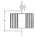
- FIG. 1 is a schematic diagram of a parallel test structure as used in the method of the present invention.
- FIG. 3 is a graph of the current through 3 series and 3 parallel interconnects as a function of time.
- FIG. 7 is a graph of the cumulative failure plot of the failure times of the parallel interconnects from simulation 9 in table III.
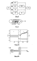
- FIG. 8 represents a block diagram of a Median Time to Failure test system.
- FIG. 9 represents a scheme of a gastube oven.
- FIG. 12 is a graph of the current profile, resistance and oven temperature change versus time of the MTF test system (left) and the conventional system (right) for determining the current density exponent n.
- This specification discloses a method for determining time to failure characteristics of a metal interconnect using a test structure comprising a plurality of such interconnects. From a statistical point of view, a series connection of metal interconnects is the optimum configuration for the reliability tests, because the same current passes through all the series connected metal lines. However, a series test structure may be difficult to use in practice due to technical limitations of the measurement equipment.
- test structure with a parallel configuration is used (see FIG. 1 ).
- Such a structure yields much faster reliability data to the customer than conventional structures thanks to their inherently larger statistical information. Besides the obtained reduction in measurement time it will furthermore be possible for the customer to apply less accelerating test conditions (i.e. test conditions closer to real-life). This renders the extrapolation of test data to user conditions more straightforward and reliable.
- the approach described herein allows use of only one current source for the whole test structure instead of one current source per interconnect.
- the method described herein is validated by mathematical simulation.
- simulation experiments have been carried out and further analysed by means of both the total resistance (TR) analysis and a software package for reliability data analysis.
- TR total resistance
- the former method uses the resistance of the global structure (being series or parallel connected) and is therefore called total resistance method.
- the structure which is constituted of a set of individual interconnects is treated as one structure.
- the resistance behaviour of this global structure is monitored and the time at which the failure criterion is exceeded is determined as can be seen in Table I, TR analysis.
- the second method called ‘reliability data analysis’ makes use of the behaviour of each individual interconnect that is part of the global structure which can be a parallel or series connection of the individual interconnects.
- the time to reach the failure criterion has been determined.
- a cumulative failure distribution can be derived using this information and by means of a commercially available software package the distribution parameters ( ⁇ and ⁇ ) can be determined. In practice, only the TR-analysis can be used for the series or parallel test structures.
- the resistance R(t) is the resistance of the interconnect at time t and at accelerating conditions j (current density) and T (temperature). It can be shown that ⁇ R(t)/R 0 changes linearly as a function of time.
- FC is defined as the failure criterion of an interconnect. This means that interconnects with a drift ⁇ R(t)/R 0 exceeding FC, are considered as failed.
- ⁇ ⁇ ⁇ R ⁇ ( t ) R 0 FC t F ⁇ t ( equation ⁇ ⁇ 2 )
- t F is the failure time of the interconnect.
- the studied quantity is the median of the failure times, i.e. the time where 50% of the interconnects failed, according to the failure criterion.
- the Black-model is used, which is the most intensively used extrapolation model.
- This model relates the median time to failure MT F of a set of interconnects with the temperature T (in K) and the current density j (in MA/cm 2 ).
- MT F Aj - n ⁇ exp ⁇ ( E a k B ⁇ T ) ( equation ⁇ ⁇ 3 )
- A is a material constant
- k B the Boltzmann constant
- E a the activation energy (in eV) of the thermally driven process
- n the current density exponent, which usually has a value between 1 and 3.
- ⁇ R med ′ (j 1 ,T 1 ) is the scale parameter of the lognormally distributed ⁇ R at accelerating conditions j 1 and T 1 and the shape parameter is the same for all accelerating conditions.
- N and j 0 denotes the mean current density through every interconnect at time 0, j tot the constant current density of the structure and R i (t 1 ) the resistance of the parallel structure at time t 1 .
- R i ⁇ ( t 2 ) R i ⁇ ( t 1 ) + ( R i ⁇ ( t 1 ) - R 0 ) ⁇ [ j i ⁇ ( t 1 ) j 0 ] n ( equation ⁇ ⁇ 12 )
- equation ⁇ ⁇ 12 In contrast to a series structure it is not easy to derive an equation for the failure time for the total structure. Only by simulation experiments it is possible to study the behaviour of the currents and relative resistance changes of the individual interconnects.
- the results of the simulation are analysed.
- the four estimated parameters are MT F and ⁇ for t f ⁇ log n (MT F , ⁇ ), the activation energy E a and the current density exponent n, respectively. Note that one is primarily interested in E a and n. For obtaining those values also the MT F need be determined.
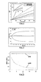
- FIG. 2 shows the relative drift DR/R for 3 series and parallel interconnects as a function of time.
- the drift velocity of interconnects that start with a relatively high resistance rise decreases, while the drift velocity of the interconnects that start with a relatively low resistance rise, increases. This is because a lower current will run through the interconnects with the highest rise of resistance, decreasing the accelerating conditions for these interconnects and therefore making these interconnects less sensitive for electromigration at this point in time. The current will then distribute over the other interconnects, making these interconnects more sensitive to EM.
- FIG. 3 the current is shown for the interconnects from FIG. 2 . Moreover, it appears that as the current density exponent n increases, the drift of the individual interconnects bow more towards each other.
- the shape parameter obtained with the reliability data analysis is in agreement with the expected value of 0.5, while for parallel interconnects the shape parameter is smaller. This is due to the fact that for the parallel interconnects, the relative resistance drifts of the individual interconnects bow towards each other, as mentioned before. For increasing n, the drifts of the parallel interconnects bend even more towards each other, thereby decreasing the shape parameter. Therefore further investigations on the dependence of the shape parameter ⁇ on several input parameters are required.
- the shape parameter obtained from the simulation experiments with reliability data analysis is denoted ⁇ par for the parallel structure and ⁇ ser for the serial structure.
- the shape parameter input value for the simulation experiments is denoted ⁇ .
- FC failure criterion
- I j ⁇ ( t ) ⁇ ⁇ ⁇ ( t )
- ⁇ 1/R> t denote the mean of the values 1/R j (t), i.e.
- a j ⁇ ( t ) a j ⁇ ⁇ 0 ⁇ [ I j ⁇ ( t ) I 0 ] n ( equation ⁇ ⁇ 20 )
- FIG. 7 shows the cumulative failure plot of the failure times for the 80 parallel interconnects of simulation experiment 9 in tables I and III.
- FIG. 8 A block diagram of the mean time to failure test system is shown in FIG. 8 . It consists of a PC, two measuring units (MU), a multiplexer (MUX), a programmable voltage source (VS), a switch box (SB), a programmable current source (CS) and a thermal unit (TU).
- a GPIB-bus interconnects the PC, the MU's, the VS and the CS.
- the thermal unit consists of a gastube oven with a sample holder and a Pt100-temperature sensor connected flow upwards of the sample holder ( FIG. 9 ).
- a gastube oven is especially used because of several features. In a gastube oven different atmospheres can be created. An atmosphere of helium can be used for example.
- the test system sequentially performs the following steps: annealing of the sample and determination of the temperature coefficient of resistance (TCR), estimation of the thermal resistance and the EM test with dynamic joule correction.
- TCR temperature coefficient of resistance
- annealing takes place, in which a small AC current is supplied to the sample, until all defects are annealed.
- the thermal resistance of the interconnect is determined at exactly the same sample temperature as during the actual EM test by supplying an AC current with the same RMS value as the DC-current of the EM test. By using this AC current, the same joule heating is created as during the EM test, but no EM damage occurs.
- the resistance of the interconnect rises rapidly due to the joule heating, as can be seen in FIG. 10 .
- the oven temperature is then lowered based on equation 25.
- a starting value has to be used for the thermal resistance, and a few iterations have to be performed to find the optimum thermal resistance value.
- the iteration is complete when the resistance value at the end of phase 2 equals the value at the end of phase 1 ( FIG. 11 ).
- the EM test is performed with a constant sample temperature by making use of equation 25 and the value of the thermal resistance as determined in phase 2 .
- v R d ( ⁇ ⁇ ⁇ R / R ) d t ⁇ ⁇ ( in ⁇ ⁇ ppm ⁇ / ⁇ s ) ( equation ⁇ ⁇ 26 )
- the current density exponent n can then easily be determined.
- an approach according to the present disclosure proposes to measure the resistance versus time while the sample temperature is raised in certain steps and the current density value is kept constant.
- An AC current is used to determine the thermal resistance every time the sample temperature is raised.
- the EM test is started by applying a DC current until the sample temperature is raised again. During this EM test the oven temperature is adjusted in order to keep the sample temperature at the desired value.
- a clear advantage of this measuring method is that the sample temperature is stable when the EM experiment is started. This is important because the activation energy is determined from the ratio of the resistance change slope at the start of the EM experiment and at the end of the previous EM experiment performed at a lower temperature.
Landscapes
- Engineering & Computer Science (AREA)
- Computer Hardware Design (AREA)
- Microelectronics & Electronic Packaging (AREA)
- General Engineering & Computer Science (AREA)
- Physics & Mathematics (AREA)
- General Physics & Mathematics (AREA)
- Environmental & Geological Engineering (AREA)
- Testing Of Individual Semiconductor Devices (AREA)
- Testing Or Measuring Of Semiconductors Or The Like (AREA)
- Investigating Or Analyzing Materials By The Use Of Electric Means (AREA)
- Carbon And Carbon Compounds (AREA)
Abstract
Description
- The present invention is related to a method for determining the lifetime characteristics of submicron metal interconnects.
- In the microelectronics industry scaling refers to the miniaturisation of active components and connections on a chip. It has followed Moore's law for many decades. Despite many advantages, scaling also strongly influences the reliability and time to failure of interconnects, i.e. the (metal) conductor lines connecting elements of the integrated circuit. Electromigration (EM), i.e. the mass transport of a metal due to the momentum transfer between conducting electrons and diffusing metal ions, is one of the most severe failure mechanisms of on-chip interconnects. A major problem when testing the reliability of new components is that their time to failure under real life conditions (Tmax=125° C.; j=1-3 105 A/cm2 for a standard type IC) is always extremely long (in order of years). For that reason, the physical failure mechanisms are studied and methods are established for accelerating these mechanisms. The failure times of the devices in operation are measured and models are developed for extrapolating these results to real life conditions. The electromigration accelerating conditions for these tests are the temperature T and the current density j. Reliability tests are usually performed on identical interconnects at accelerating conditions (j,T) (170° C.<T<350° C. and 106<j<107 A/cm2 instead of T=125° C. and j=1-3.105 A/cm2). All interconnects are each individually connected with an own power supply and provided with a multiplexer. Moreover, each interconnect can be found on a different IC package, which is an expensive and time-consuming activity. In order to derive the activation energy, which is a parameter describing the temperature dependence of the observed degradation, these tests must be performed at three temperatures, therefore tripling the number of power supplies, multiplexers and IC packages. This makes the tests more complex and expensive. Nevertheless these reliability tests are of great importance to manufacturers because on the one hand continuously operational IC's are indispensable and on the other hand the competitive strength of manufacturers strongly depends on the reliability of their products. Therefore such tests should provide a large amount of statistical information in a relatively short period of time, while keeping costs under control. It is hard to lower the costs without decreasing the accuracy of the experiments. To solve this problem one need to look for a test structure that can provide a large amount of accurate data in a short period of time at low cost.
- Patent document US-2002/0017906-A1 discloses a method for detecting early failures in a large ensemble of semiconductor elements. It employs a parallel test structure. A Wheatstone bridge arrangement is used to measure small resistance changes. The criterion for failure of the test structure is the time to first discernible voltage imbalance ΔV(t).
- The present disclosure aims to provide a method for determining the time to failure that allows manufacturers to perform reliability tests in a relatively fast and inexpensive way.
- The disclosure relates to a method for determining time to failure characteristics of an on-chip interconnect subject to electromigration. One such method includes the steps of
-
- providing a test structure, being a parallel connection of a plurality of such on-chip interconnects,
- performing measurements on the test structure under test conditions for current density and temperature, the test structure being such that failure of one of the on-chip interconnects within the parallel connection changes the test conditions for at least one of the other individual on-chip interconnects of the parallel connection,
- determining from the measurements estimates of the time to failure characteristics, whereby the change in the test conditions is compensated for.
- Preferably the step of determining is based on fitting. Advantageously the current density exponent n and the activation energy Ea are determined with the fitting.
- The time to failure characteristics preferably include the median time to failure of the on-chip interconnects as well as the shape parameter.
- In a preferred embodiment the method further comprises a step of correcting the shape parameter estimation, the shape parameter being determined by fitting. The step of correcting the shape parameter is advantageously performed via a predetermined relationship.
- Preferably the parallel connection of the on-chip interconnects is within a single package.
- In an alternative embodiment the method further comprises the step of performing measurements on the individual devices, belonging to the parallel connection. The step of compensating typically includes correcting the measurements on the individual interconnects.
- The measurements advantageously are performed with electromigration accelerating test conditions for current density and temperature.
- In an another advantageous embodiment the determining step includes the step of determining the time to failure characteristics under real life conditions by extrapolation. The extrapolation typically uses the Black model, which is used to describe the temperature and current dependency of the observed degradation.
- The measurements are advantageously resistance change measurements.
- In a specific embodiment the electromigration acceleratering test conditions are used as input values.
- Further the number of interconnects within parallel connection may be used as input value. Also the failure criterion can be used as input.
- Preferably the measurements are performed at several time instances. Advantageously the measurements are performed at least three different temperatures.
- In a preferred embodiment the on-chip interconnect is in a 90 nm technology. Alternatively it is in a sub90 nm technology.
- The invention also relates to a program, executable on a programmable device containing instructions, which when executed, perform the method as described before.
-
FIG. 1 is a schematic diagram of a parallel test structure as used in the method of the present invention. -
FIG. 2 is a graph of the relative drift for 3 series and parallel interconnects as a function of time for n=2. -
FIG. 3 is a graph of the current through 3 series and 3 parallel interconnects as a function of time. -
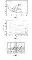
FIG. 4 is a graph of σpar/σ and σ ser/σ as a function of n for several input values of σ (0.1 till 1.0) and with a fixed FC=1, where σpar and σser are respectively the shape parameter for the parallel and series interconnects gained from the simulation experiments. σ is the input parameter for the simulation experiments. -
FIG. 5 is a graph of σpar/σ and σser/σ as a function of n for σ=0.5 and with FC varying from 0.5 to 3. -
FIG. 6 is a graph of σpar/σ as a function of FC for σ=0.5 and with n varying from 1 to 20. -
FIG. 7 is a graph of the cumulative failure plot of the failure times of the parallel interconnects from simulation 9 in table III. -
FIG. 8 represents a block diagram of a Median Time to Failure test system. -
FIG. 9 represents a scheme of a gastube oven. -
FIG. 10 is a graph of the evolution of the interconnect resistance and the oven temperature (Ti=180° C., I=25 mA) (FIG. 10 a) and a current profile of the test (FIG. 10 b). -
FIG. 11 a is a graph of the evolution of the resistance andFIG. 11 b the temperature versus time during a test (IAC=10 mA, Ts=100° C.). -
FIG. 12 is a graph of the current profile, resistance and oven temperature change versus time of the MTF test system (left) and the conventional system (right) for determining the current density exponent n. - This specification discloses a method for determining time to failure characteristics of a metal interconnect using a test structure comprising a plurality of such interconnects. From a statistical point of view, a series connection of metal interconnects is the optimum configuration for the reliability tests, because the same current passes through all the series connected metal lines. However, a series test structure may be difficult to use in practice due to technical limitations of the measurement equipment.
- Alternatively, a test structure with a parallel configuration is used (see
FIG. 1 ). Such a structure yields much faster reliability data to the customer than conventional structures thanks to their inherently larger statistical information. Besides the obtained reduction in measurement time it will furthermore be possible for the customer to apply less accelerating test conditions (i.e. test conditions closer to real-life). This renders the extrapolation of test data to user conditions more straightforward and reliable. As an additional advantage, the approach described herein allows use of only one current source for the whole test structure instead of one current source per interconnect. - The method described herein is validated by mathematical simulation. In order to calculate and to compare the behaviour of parallel and/or series test structures, simulation experiments have been carried out and further analysed by means of both the total resistance (TR) analysis and a software package for reliability data analysis. The former method uses the resistance of the global structure (being series or parallel connected) and is therefore called total resistance method. The structure which is constituted of a set of individual interconnects is treated as one structure. The resistance behaviour of this global structure is monitored and the time at which the failure criterion is exceeded is determined as can be seen in Table I, TR analysis. The second method called ‘reliability data analysis’ makes use of the behaviour of each individual interconnect that is part of the global structure which can be a parallel or series connection of the individual interconnects. For each individual interconnect, the time to reach the failure criterion has been determined. A cumulative failure distribution can be derived using this information and by means of a commercially available software package the distribution parameters (μ and σ) can be determined. In practice, only the TR-analysis can be used for the series or parallel test structures.
- The parameter studied during the accelerating conditions is the relative resistance change, defined as
The resistance R(t) is the resistance of the interconnect at time t and at accelerating conditions j (current density) and T (temperature). It can be shown that ΔR(t)/R0 changes linearly as a function of time. FC is defined as the failure criterion of an interconnect. This means that interconnects with a drift ΔR(t)/R0 exceeding FC, are considered as failed. Subsequently,
where tF is the failure time of the interconnect. The studied quantity is the median of the failure times, i.e. the time where 50% of the interconnects failed, according to the failure criterion. - For extrapolation of the simulation results to more real life conditions, the Black-model is used, which is the most intensively used extrapolation model. This model relates the median time to failure MTF of a set of interconnects with the temperature T (in K) and the current density j (in MA/cm2).
where A is a material constant, kB the Boltzmann constant, Ea the activation energy (in eV) of the thermally driven process and n the current density exponent, which usually has a value between 1 and 3. - For a typical test a set of N interconnects is taken with accelerating conditions j and T. It is assumed that both j and T are constant and that the failure times of the interconnects obey to a monomodal distribution. Moreover, a lognormal distribution is taken, because it is the far most commonly used distribution, i.e. tf∝ log n(ν,σ). So, the natural logarithm of tf, ln(tf), has a normal distribution. Moreover, its mean μ is given by the natural logarithm of the median time to failure. The median time to failure and σ are called the scale and shape parameter of the distributed failure times, respectively. Given the 1-to-1 relationship between the mean μ of a lognormal distribution and the median time to failure MTF, further on the notation log n (MTF, σ) is applied, which clearly is to be interpreted as log n (μ=ln(MTF), σ). Due to transformations of statistical distributions, the relative resistance ΔR is lognormally distributed, ΔR ∝ log n (ΔRmed′,σ), with median ΔRmed′ given by
The shape parameter σ is the same as for the failure times. At higher accelerating conditions (different j or T), the resistance change per unit of time is also lognormally distributed. Using the Black equation (3), the scale parameter ΔRmed′ (j,T) at higher accelerating conditions can be written as
where ΔRmed′ (j1,T1) is the scale parameter of the lognormally distributed ΔR at accelerating conditions j1 and T1 and the shape parameter is the same for all accelerating conditions. - The simulation of a series electromigration test structure of N parallel interconnects is quite simple. For this structure, the current density j in equation (3) is assumed constant as a function of time and as a consequence, for each interconnection, the resistance change per unit of time DRi(t)=DRi(1) is also constant as a function of time. Moreover, DRi(t)∝ log n(ΔRmed′, σ). Taking for simplicity Ri(t=0) for interconnect i at a constant level R0, ∀i, the resistance for each interconnection per unit of time is given by
R i(t)=R 0 +t·DR i(1) (equation 6)
Using equations (2) and (6), the relative resistance change for the total structure is
where μ′ is the mean of the lognormally distributed DRi(1) values for the N interconnects. Subsequently, the failure time of the total series structure can be approximated by - For parallel structures, where the current density ji is not constant, the situation is far more complicated. The resistance Ri and the current density ji of the ith interconnection after 1 time unit t1, respectively, are given by
where i=1, . . . , N and j0 denotes the mean current density through every interconnect attime 0, jtot the constant current density of the structure and Ri(t1) the resistance of the parallel structure at time t1. At time t2=2t1, it is assumed that the current density does not change during this step, so
In contrast to a series structure it is not easy to derive an equation for the failure time for the total structure. Only by simulation experiments it is possible to study the behaviour of the currents and relative resistance changes of the individual interconnects. - The results of the simulation are analysed. The four estimated parameters are MTF and σ for tf∝ log n (MTF,σ), the activation energy Ea and the current density exponent n, respectively. Note that one is primarily interested in Ea and n. For obtaining those values also the MTF need be determined. For the simulation experiments N interconnects in a series and/or parallel structure are taken with length L=2000 μm, thickness d=0.5 μm, width b=0.5 μm, resistivity ρA1=2.68 μΩcm, current density j1=2MA/cm2, temperature T1=200° C., current density exponent n=2, activation energy Ea=0.8 eV, failure times tf ∝ log n (200, 0.5), failure criterion FC=1 and 500 time steps of 1 hour as standard input values.
- A. Relative Resistance Change for Series and Parallel Interconnects
- For the series interconnects the relative resistance drift of the interconnects increases linearly, while for the parallel interconnects the relative resistance drift of the individual interconnects bends towards each other.
FIG. 2 shows the relative drift DR/R for 3 series and parallel interconnects as a function of time. The drift velocity of interconnects that start with a relatively high resistance rise, decreases, while the drift velocity of the interconnects that start with a relatively low resistance rise, increases. This is because a lower current will run through the interconnects with the highest rise of resistance, decreasing the accelerating conditions for these interconnects and therefore making these interconnects less sensitive for electromigration at this point in time. The current will then distribute over the other interconnects, making these interconnects more sensitive to EM. InFIG. 3 the current is shown for the interconnects fromFIG. 2 . Moreover, it appears that as the current density exponent n increases, the drift of the individual interconnects bow more towards each other. - B. Influence of the Current Density Exponent
- Table I shows the scale parameters MTF and shape parameters σ estimations for 80 parallel and series interconnects as a function of the current density exponent n, using FC=1.
TABLE I Reliability data analysis TR-Analyse Series Parallel Series parallel n = 1, 2, 3 n = 1 n = 2 n = 3 n = 1, 2, 3 n = 1 , 2, 3 sim MTF σ MTF σ MTF σ MTF σ Tf tf 1 193 0.522 191 0.403 191 0.317 191 0.256 168 196 2 187 0.464 184 0.355 184 0.279 185 0.225 167 188 3 204 0.402 204 0.323 204 0.254 204 0.204 169 207 4 202 0.453 200 0.358 200 0.283 201 0.229 180 205 5 209 0.476 207 0.373 207 0.293 208 0.236 187 212 6 196 0.504 194 0.393 192 0.262 195 0.252 172 199 7 203 0.437 202 0.339 203 0.274 203 0.222 185 207 8 220 0.457 218 0.358 218 0.282 220 0.227 197 223 9 200 0.505 198 0.394 198 0.31 199 0.25 176 203 10 202 0.44 202 0.35 202 0.275 202 0.222 184 206 11 214 0.472 213 0.366 213 0.286 213 0.23 193 217 12 209 0.481 209 0.38 209 0.3 209 0.242 187 214 13 196 0.491 195 0.384 195 0.302 195 0.244 174 199 14 193 0.484 190 0.368 190 0.289 191 0.233 171 194 15 186 0.469 185 0.367 185 0.295 186 0.237 167 189 16 194 0.454 191 0.347 191 0.273 192 0.22 174 195 17 182 0.511 181 0.409 181 0.322 182 0.26 159 186 18 203 0.399 201 0.302 201 0.237 202 0.191 188 204 19 204 0.466 202 0.364 202 0.286 203 0.231 183 207 20 188 0.453 185 0.344 185 0.27 186 0.217 169 189 mean 199 0.47 198 0.364 198 0.284 198 0.231 179 202 error 9 0.032 7 0.026 6 0.021 5 0.016 10 10 - It is to be noted that μ for both series and parallel interconnects agree with the proposed median failure time of 200 hours of the individual interconnects used as an input parameter for the simulated data. Table I shows that for every current density exponent n, the failure time of the total parallel structure (with FC=1) agrees with said value of 200 hours for the scale parameter MTF. This means that a parallel EM test structure is a correct approach for the determination of the failure time of submicron interconnects. For the total series structure, the failure time of the total structure deviates from the proposed value for MTF of the individual interconnects. This can easily be explained by the asymmetry of the distributed failure times and using equations (7) and (8).
- For series interconnects the shape parameter obtained with the reliability data analysis is in agreement with the expected value of 0.5, while for parallel interconnects the shape parameter is smaller. This is due to the fact that for the parallel interconnects, the relative resistance drifts of the individual interconnects bow towards each other, as mentioned before. For increasing n, the drifts of the parallel interconnects bend even more towards each other, thereby decreasing the shape parameter. Therefore further investigations on the dependence of the shape parameter σ on several input parameters are required.
- The shape parameter obtained from the simulation experiments with reliability data analysis is denoted σpar for the parallel structure and σser for the serial structure. The shape parameter input value for the simulation experiments is denoted σ.
FIG. 4 shows respectively σpar and σser divided by the input value σ for the simulation experiments as a function of n for several values of σ and with a fixed failure criterion FC=1. For the series structure σser/σ is independent of n for several values of σ. For the parallel structure a fixed relationship of σpar/σ as a function of n can be found for several values of σ. This means that for a fixed FC value, a certain relationship of σpar/σ as a function of n can be found, independent of the input value σ. - To determine the influence of the failure criterion FC on σpar/σ as a function of n, simulation experiments were carried out with a fixed σ=0.5 and with FC varying from 0.5 to 3. The results are shown in
FIG. 5 . The results show that the shape of the curves for different FC values doesn't change. For FC>1, the curves move more away from 1, while the opposite is true for FC<1.FIG. 6 shows the relationship between σpar/σ and FC for different values of n. It is shown that σpar/σ decreases in the same way, but that for different n, the relationship shifts more towards or more away from 1. - As a consequence of these results, using both
FIGS. 5 and 6 , and knowing both n and FC, it is possible to estimate the correct shape parameter for parallel test structures. This information extracted from the simulation experiments can be used to correct the shape parameter for real time experiments. However, the method described above may be rather tedious, because every relationship between σpar/σ and n must be known for all FC values, which is a time-consuming activity. Moreover, the acquired corrected value for σpar by applying this method is only a rough estimation of the real value. The method further requires that for each interconnect info on R and I are to be kept. In order to get a more accurate value for the shape parameter, an alternative method is proposed for the correction of the experimental data gained from a parallel structure. More in particular, the alternative method will yield an improved estimate of the shape parameter. - Still a parallel structure of N interconnects is considered. At every moment in time it is known that
ΔV(t)=R j(t)·I j(t) (equation 13)
where Rj(t) and Ij(t) are the resistance and current value, respectively, of interconnect j at time t. Furthermore,
Subsequently,
Let <1/R>t denote the mean of thevalues 1/Rj(t), i.e.
Moreover, if I0=Itot/N denotes the mean current per interconnect, equation (15) can be written as
As already mentioned previously, ΔR(t)/R0 changes linearly as a function of time:
where a is a constant.
Subsequently, for every interconnect j, one can write that
Where FC and (tF)j are the failure criterion and the failure time of the jth interconnect, respectively. Postulate aj=aj(t) as a function of time t, temperature T and current I. In agreement with the Black equation, one can then write
aj0 is the coefficient for interconnect j, with current I=I0 and a certain temperature T.
a j0 =a j(I=I 0 ,T) (equation 21)
Combining equations (19) and (20)
Substitution of equation (17) in equation (22) gives
With this equation, it is possible to recalculate the aj0 value. In practice, all Rj(t) are known and subsequently also the <1/R>t values at every t. The only concern is to determine the derivative of the Rj(t) values. In practice, several techniques to determine the derivative of Rj(t) are available. If both Rj(t) and its derivative are known, the right side of equation can be calculated for every t value. If then a straight line is fitted through the corrected points, the slope of this straight line gives the aj0 value for interconnect j. Because aj=FC/(tf)j, the correct failure times can be determined with the correct MTF and σ. - The theoretical verification of this method can be achieved by applying it to the data gained from simulation experiments on parallel structures. The simulations are performed in exactly the same conditions as for obtaining the experimental results of Table I. Table II shows the MTF and σ values, which were estimated from the simulation data of both parallel and corrected structures. Note that the corrected data from the simulation experiments on parallel structures is in good agreement with the expected values for MTF (=200) and σ (=0.5), used as input parameters for the simulation experiments. This shows this method can correct the data gained from parallel test structures.
TABLE II Parallel Correction n = 1 n = 2 n = 3 n = 1 n = 2 n = 3 sim MTF σ MTF σ MTF σ MTF σ MTF σ MTF σ 1 212 0.35 212 0.274 213 0.221 214 0.454 214 0.454 214 0.454 2 211 0.373 211 0.294 212 0.237 212 0.468 212 0.468 212 0.468 3 217 0.383 217 0.307 218 0.244 218 0.486 218 0.486 218 0.486 4 202 0.367 202 0.289 203 0.233 205 0.479 205 0.479 205 0.479 5 185 0.359 185 0.282 186 0.227 188 0.469 188 0.469 188 0.469 6 208 0.392 208 0.308 209 0.248 210 0.501 210 0.501 210 0.501 7 188 0.393 188 0.309 188 0.249 190 0.506 190 0.506 190 0.506 8 208 0.334 208 0.268 209 0.216 208 0.424 208 0.424 208 0.424 9 212 0.374 212 0.295 213 0.238 212 0.468 212 0.468 212 0.468 10 190 0.377 190 0.296 191 0.239 192 0.486 192 0.486 192 0.486 11 179 0.369 179 0.291 180 0.235 181 0.471 181 0.471 181 0.471 12 198 0.353 198 0.283 198 0.221 199 0.443 199 0.443 199 0.443 13 196 0.422 196 0.334 197 0.269 197 0.532 197 0.532 197 0.532 14 180 0.385 180 0.286 180 0.231 182 0.476 182 0.476 182 0.476 15 206 0.365 206 0.287 207 0.231 209 0.741 209 0.741 209 0.741 16 189 0.409 189 0.321 190 0.259 191 0.525 191 0.525 191 0.525 17 208 0.434 208 0.344 209 0.278 211 0.55 211 0.55 211 0.55 18 197 0.394 197 0.310 197 0.250 198 0.501 198 0.501 198 0.501 19 191 0.396 191 0.314 192 0.253 192 0.497 192 0.497 192 0.497 20 184 0.343 184 0.269 184 0.216 186 0.455 186 0.455 186 0.455 mean 198 0.379 198 0.298 199 0.240 200 0.497 200 0.497 200 0.497 error 8 0.026 6 0.022 5 0.018 10 0.033 10 0.033 10 0.033
C. Determination of Activation Energies Ea - Consider a system driven by only 1 activation energy (Ea=0.8 eV), which in practice is mostly the case. Suppose the failure time tF of the interconnects at accelerating conditions j1=2MA/cm2 and T1=200° C. is lognormally distributed with MTF1=200 and σ=0.5 using FC=1. At
higher temperatures 220° C. and 240° C., the scale parameters can be calculated using equation (7). Table III shows the activation energies calculated via the Black equation for both series and parallel test structures, using the TR-analysis and the software package for 80 series and parallel interconnects (n=2).TABLE III “Failure” analysis TR-analysis n = 2 n = 2 n = 2 n = 2 series parallel series Parallel Sim Ea Ea Ea Ea 1 0.772 0.774 0.772 0.774 2 0.746 0.749 0.761 0.745 3 0.876 0.884 0.894 0.881 4 0.757 0.759 0.743 0.761 5 0.817 0.822 0.825 0.82 6 0.752 0.756 0.747 0.756 7 0.805 0.814 0.843 0.808 8 0.815 0.821 0.831 0.818 9 0.802 0.806 0.806 0.806 10 0.805 0.814 0.831 0.810 11 0.809 0.812 0.804 0.813 12 0.858 0.866 0.875 0.863 13 0.854 0.86 0.879 0.855 14 0.792 0.792 0.791 0.791 15 0.759 0.765 0.767 0.764 16 0.778 0.783 0.809 0.776 17 0.718 0.725 0.724 0.724 18 0.801 0.804 0.827 0.799 19 0.793 0.796 0.790 0.796 20 0.778 0.781 0.803 0.776 mean 0.79 0.80 0.81 0.80 error 0.02 0.02 0.1 0.1 - For both methods the mean values of the activation energies agree very well the proposed value of 0.8 eV that was an input parameter for the simulated data. This implies that for the monomodal lognormally distributed failure times, both series and parallel test structures can be used for the determination of both the activation energy and the current density exponent n. Also n is computed via the Black equation.
FIG. 7 shows the cumulative failure plot of the failure times for the 80 parallel interconnects of simulation experiment 9 in tables I and III. - As already mentioned before, the current density and the temperature of the sample have to remain constant during the entire test in order to guarantee an accurate time to failure determination. To keep the temperature of the sample constant during the entire test, the joule heating of the interconnect has to be taken into account, Joule heating is created when a current is applied to the interconnect. The interconnect temperature is given by the following equation:
T i =T o +P Eiθi with PEi=IDC 2Ri (equation 25)
where Ti is the actual temperature of the interconnect, To the oven temperature, PEi the power dissipated by the interconnect, θi the thermal resistance and Ri the electrical resistance of each interconnect. - In conventional median time to failure (MTF) tests the joule heating of the interconnect is estimated and the oven temperature is decreased with the estimated value of the joule heating in the beginning of the test, but this is not sufficient. During the electromigration (EM) test the resistance of the interconnect increases and so the joule heating also increases. From
equation 25 it can be concluded that the interconnect temperature will increase, thus giving rise to the acceleration of the EM process. - This problem can be solved by using an AC current based dynamic joule correction, by which no EM damage occurs. During the determination of the thermal resistance of the interconnect the same temperature and the same RMS value of the current is used as in the proper EM test. This approach is described with more details in the following paragraphs.
- A block diagram of the mean time to failure test system is shown in
FIG. 8 . It consists of a PC, two measuring units (MU), a multiplexer (MUX), a programmable voltage source (VS), a switch box (SB), a programmable current source (CS) and a thermal unit (TU). A GPIB-bus interconnects the PC, the MU's, the VS and the CS. The thermal unit consists of a gastube oven with a sample holder and a Pt100-temperature sensor connected flow upwards of the sample holder (FIG. 9 ). A gastube oven is especially used because of several features. In a gastube oven different atmospheres can be created. An atmosphere of helium can be used for example. From the different measurements a place is determined where the Pt100-temperature sensor picks up only 1% of the joule heating of the sample and where the temperature relationship To(Ts) is stable, To being the oven temperature and Ts the sample temperature measured by the Pt100-temperature sensor. - For the EM test the test system sequentially performs the following steps: annealing of the sample and determination of the temperature coefficient of resistance (TCR), estimation of the thermal resistance and the EM test with dynamic joule correction. During the first step (
FIG. 10 ) annealing takes place, in which a small AC current is supplied to the sample, until all defects are annealed. During the second step the thermal resistance of the interconnect is determined at exactly the same sample temperature as during the actual EM test by supplying an AC current with the same RMS value as the DC-current of the EM test. By using this AC current, the same joule heating is created as during the EM test, but no EM damage occurs. When the high AC current is applied, the resistance of the interconnect rises rapidly due to the joule heating, as can be seen inFIG. 10 . The oven temperature is then lowered based onequation 25. A starting value has to be used for the thermal resistance, and a few iterations have to be performed to find the optimum thermal resistance value. The iteration is complete when the resistance value at the end ofphase 2 equals the value at the end of phase 1 (FIG. 11 ). During the last step the EM test is performed with a constant sample temperature by making use ofequation 25 and the value of the thermal resistance as determined inphase 2. - This approach has several advantages: no temperature change occurs at the start of the EM experiment, the thermal resistance is determined at the actual test temperature and the TCR determination is not needed for the determination of the thermal resistance. Further the current density exponent n and the activation energy Ea can be determined with high accuracy. This will be detailed subsequently.
- As already discussed previously, conventional methods make use of the cross-cut technique to determine the acceleration parameters. Due to the inherent statistical scattering of the degradation curves, a lot of samples are needed to get rid of the statistical effects. These statistical effects can be excluded by using only one sample to complete the determination of the acceleration parameters Ea and n. To determine the current density exponent the interconnect resistance is measured during several current density values. It is very important that here also the sample temperature remains the same, therefore the AC-current is used to determine the thermal resistance of the interconnect at a certain current density. When the thermal resistance is known, the EM test is performed until the current density is raised again (
FIG. 12 ). - A clear benefit of this approach is that no temperature change occurs at the start of the EM experiment. This is particularly important due to the fact that the current density exponent is determined by the ratio of the resistance change slope at the start of the EM experiment and at the end of the previous EM experiment performed at a lower current. This ratio is important for defining the velocity of resistance change (vR).
The parameter vR is inversely proportional to the time to failure:
v R =A′·j n ·e−E/kT with A′ a constant (equation 27)
The current density exponent n can then easily be determined. - Whereas conventional systems keep the current density constant and raise the oven temperature in certain steps in order to estimate the activation energy, an approach according to the present disclosure proposes to measure the resistance versus time while the sample temperature is raised in certain steps and the current density value is kept constant. An AC current is used to determine the thermal resistance every time the sample temperature is raised. When the thermal resistance is known the EM test is started by applying a DC current until the sample temperature is raised again. During this EM test the oven temperature is adjusted in order to keep the sample temperature at the desired value.
- A clear advantage of this measuring method is that the sample temperature is stable when the EM experiment is started. This is important because the activation energy is determined from the ratio of the resistance change slope at the start of the EM experiment and at the end of the previous EM experiment performed at a lower temperature.
Claims (12)
Applications Claiming Priority (4)
| Application Number | Priority Date | Filing Date | Title |
|---|---|---|---|
| EP04447117A EP1596210A1 (en) | 2004-05-11 | 2004-05-11 | Method for lifetime determination of submicron metal interconnects |
| EP04447117 | 2004-05-11 | ||
| EP04447117.5 | 2004-05-11 | ||
| PCT/BE2005/000076 WO2005109018A1 (en) | 2004-05-11 | 2005-05-11 | Method for determining time to failure of submicron metal interconnects |
Publications (2)
| Publication Number | Publication Date |
|---|---|
| US20080098270A1 true US20080098270A1 (en) | 2008-04-24 |
| US8030099B2 US8030099B2 (en) | 2011-10-04 |
Family
ID=34933034
Family Applications (1)
| Application Number | Title | Priority Date | Filing Date |
|---|---|---|---|
| US11/596,264 Expired - Fee Related US8030099B2 (en) | 2004-05-11 | 2005-05-11 | Method for determining time to failure of submicron metal interconnects |
Country Status (5)
| Country | Link |
|---|---|
| US (1) | US8030099B2 (en) |
| EP (2) | EP1596210A1 (en) |
| AT (1) | ATE476669T1 (en) |
| DE (1) | DE602005022722D1 (en) |
| WO (1) | WO2005109018A1 (en) |
Cited By (6)
| Publication number | Priority date | Publication date | Assignee | Title |
|---|---|---|---|---|
| CN102955121A (en) * | 2012-10-30 | 2013-03-06 | 工业和信息化部电子第五研究所 | Residual life predication method and device for electromigration failure |
| US8543967B2 (en) | 2012-02-24 | 2013-09-24 | Avago Technologies General Ip (Singapore) Pte. Ltd. | Computer system and method for determining a temperature rise in direct current (DC) lines caused by joule heating of nearby alternating current (AC) lines |
| US20160363623A1 (en) * | 2015-06-10 | 2016-12-15 | Qualcomm Incorporated | Method and apparatus for integrated circuit monitoring and prevention of electromigration failure |
| CN106449460A (en) * | 2016-10-26 | 2017-02-22 | 上海华力微电子有限公司 | A current acceleration factor assessment method in a constant temperature electromigration test |
| US20170356957A1 (en) * | 2016-06-14 | 2017-12-14 | Cascade Microtech, Inc. | Systems and methods for electrically testing electromigration in an electromigration test structure |
| US10732216B2 (en) | 2012-10-30 | 2020-08-04 | Fifth Electronics Research Institute Of Ministry Of Industry And Information Technology | Method and device of remaining life prediction for electromigration failure |
Families Citing this family (2)
| Publication number | Priority date | Publication date | Assignee | Title |
|---|---|---|---|---|
| US10634714B2 (en) * | 2016-02-23 | 2020-04-28 | Intel Corporation | Apparatus and method for monitoring and predicting reliability of an integrated circuit |
| CN118795392B (en) * | 2024-09-11 | 2024-11-29 | 嘉兴翼波电子有限公司 | A solderless edge mounted connector and its testing system |
Citations (12)
| Publication number | Priority date | Publication date | Assignee | Title |
|---|---|---|---|---|
| US5264377A (en) * | 1990-03-21 | 1993-11-23 | At&T Bell Laboratories | Integrated circuit electromigration monitor |
| US5497076A (en) * | 1993-10-25 | 1996-03-05 | Lsi Logic Corporation | Determination of failure criteria based upon grain boundary electromigration in metal alloy films |
| US6037795A (en) * | 1997-09-26 | 2000-03-14 | International Business Machines Corporation | Multiple device test layout |
| US6163288A (en) * | 1997-10-09 | 2000-12-19 | Kabushiki Kaisha Toshiba | Digital-to-analog converter in which an analog output of low order bits is attenuated, and added to an analog output of high order bits |
| US20020017906A1 (en) * | 2000-04-17 | 2002-02-14 | Ho Paul S. | Electromigration early failure distribution in submicron interconnects |
| US20030231123A1 (en) * | 2002-06-14 | 2003-12-18 | Dell Products L.P. | Information handling system with self-calibrating digital-to-analog converter |
| US20040051553A1 (en) * | 2002-09-13 | 2004-03-18 | Chartered Semiconductor Manufacturing Ltd. | Test structures for on-chip real-time reliability testing |
| US6714037B1 (en) * | 2002-06-25 | 2004-03-30 | Advanced Micro Devices, Inc. | Methodology for an assessment of the degree of barrier permeability at via bottom during electromigration using dissimilar barrier thickness |
| US6770847B2 (en) * | 2002-09-30 | 2004-08-03 | Advanced Micro Devices, Inc. | Method and system for Joule heating characterization |
| US20040220775A1 (en) * | 2003-04-29 | 2004-11-04 | Schuh William C | Detecting thermocouple failure using loop resistance |
| US20040239544A1 (en) * | 2002-04-25 | 2004-12-02 | Yingxuan Li | Circuit, apparatus and method for improved current distribution of output drivers enabling improved calibration efficiency and accuracy |
| US20050030214A1 (en) * | 2003-07-07 | 2005-02-10 | Seiko Epson Corporation | Digital-to-analog converting circuit, electrooptical device, and electronic apparatus |
Family Cites Families (3)
| Publication number | Priority date | Publication date | Assignee | Title |
|---|---|---|---|---|
| GB2176653B (en) * | 1985-06-20 | 1988-06-15 | Gen Electric Plc | Method of manufacturing integrated circuits |
| NL8902891A (en) * | 1989-04-19 | 1990-11-16 | Imec Inter Uni Micro Electr | METHOD AND APPARATUS FOR ACCELERATING THE AGING OF ONE OR MORE ELEMENTS WITH AN ELECTROMAGNETIC AGING PARAMETER |
| DE4003682A1 (en) | 1990-02-07 | 1991-08-08 | Steinheil Optronik Gmbh | Rapid, high resolution D=A converter - measures sequential output signal at high velocity during intermediate matching operation |
-
2004
- 2004-05-11 EP EP04447117A patent/EP1596210A1/en not_active Withdrawn
-
2005
- 2005-05-11 DE DE602005022722T patent/DE602005022722D1/en not_active Expired - Lifetime
- 2005-05-11 US US11/596,264 patent/US8030099B2/en not_active Expired - Fee Related
- 2005-05-11 EP EP05745292A patent/EP1771743B1/en not_active Expired - Lifetime
- 2005-05-11 AT AT05745292T patent/ATE476669T1/en not_active IP Right Cessation
- 2005-05-11 WO PCT/BE2005/000076 patent/WO2005109018A1/en not_active Ceased
Patent Citations (13)
| Publication number | Priority date | Publication date | Assignee | Title |
|---|---|---|---|---|
| US5264377A (en) * | 1990-03-21 | 1993-11-23 | At&T Bell Laboratories | Integrated circuit electromigration monitor |
| US5497076A (en) * | 1993-10-25 | 1996-03-05 | Lsi Logic Corporation | Determination of failure criteria based upon grain boundary electromigration in metal alloy films |
| US6037795A (en) * | 1997-09-26 | 2000-03-14 | International Business Machines Corporation | Multiple device test layout |
| US6163288A (en) * | 1997-10-09 | 2000-12-19 | Kabushiki Kaisha Toshiba | Digital-to-analog converter in which an analog output of low order bits is attenuated, and added to an analog output of high order bits |
| US20020017906A1 (en) * | 2000-04-17 | 2002-02-14 | Ho Paul S. | Electromigration early failure distribution in submicron interconnects |
| US20040239544A1 (en) * | 2002-04-25 | 2004-12-02 | Yingxuan Li | Circuit, apparatus and method for improved current distribution of output drivers enabling improved calibration efficiency and accuracy |
| US20030231123A1 (en) * | 2002-06-14 | 2003-12-18 | Dell Products L.P. | Information handling system with self-calibrating digital-to-analog converter |
| US6822473B1 (en) * | 2002-06-25 | 2004-11-23 | Advanced Micro Devices, Inc. | Determination of permeability of layer material within interconnect |
| US6714037B1 (en) * | 2002-06-25 | 2004-03-30 | Advanced Micro Devices, Inc. | Methodology for an assessment of the degree of barrier permeability at via bottom during electromigration using dissimilar barrier thickness |
| US20040051553A1 (en) * | 2002-09-13 | 2004-03-18 | Chartered Semiconductor Manufacturing Ltd. | Test structures for on-chip real-time reliability testing |
| US6770847B2 (en) * | 2002-09-30 | 2004-08-03 | Advanced Micro Devices, Inc. | Method and system for Joule heating characterization |
| US20040220775A1 (en) * | 2003-04-29 | 2004-11-04 | Schuh William C | Detecting thermocouple failure using loop resistance |
| US20050030214A1 (en) * | 2003-07-07 | 2005-02-10 | Seiko Epson Corporation | Digital-to-analog converting circuit, electrooptical device, and electronic apparatus |
Cited By (9)
| Publication number | Priority date | Publication date | Assignee | Title |
|---|---|---|---|---|
| US8543967B2 (en) | 2012-02-24 | 2013-09-24 | Avago Technologies General Ip (Singapore) Pte. Ltd. | Computer system and method for determining a temperature rise in direct current (DC) lines caused by joule heating of nearby alternating current (AC) lines |
| CN102955121A (en) * | 2012-10-30 | 2013-03-06 | 工业和信息化部电子第五研究所 | Residual life predication method and device for electromigration failure |
| US9952275B2 (en) | 2012-10-30 | 2018-04-24 | Fifth Electronics Research Institute Of Ministry Of Industry And Information Technology | Method and device of remaining life prediction for electromigration failure |
| US10732216B2 (en) | 2012-10-30 | 2020-08-04 | Fifth Electronics Research Institute Of Ministry Of Industry And Information Technology | Method and device of remaining life prediction for electromigration failure |
| US20160363623A1 (en) * | 2015-06-10 | 2016-12-15 | Qualcomm Incorporated | Method and apparatus for integrated circuit monitoring and prevention of electromigration failure |
| US10591531B2 (en) * | 2015-06-10 | 2020-03-17 | Qualcomm Incorporated | Method and apparatus for integrated circuit monitoring and prevention of electromigration failure |
| US20170356957A1 (en) * | 2016-06-14 | 2017-12-14 | Cascade Microtech, Inc. | Systems and methods for electrically testing electromigration in an electromigration test structure |
| US10161994B2 (en) * | 2016-06-14 | 2018-12-25 | Formfactor Beaverton, Inc. | Systems and methods for electrically testing electromigration in an electromigration test structure |
| CN106449460A (en) * | 2016-10-26 | 2017-02-22 | 上海华力微电子有限公司 | A current acceleration factor assessment method in a constant temperature electromigration test |
Also Published As
| Publication number | Publication date |
|---|---|
| US8030099B2 (en) | 2011-10-04 |
| EP1771743B1 (en) | 2010-08-04 |
| EP1596210A1 (en) | 2005-11-16 |
| EP1771743A1 (en) | 2007-04-11 |
| DE602005022722D1 (en) | 2010-09-16 |
| ATE476669T1 (en) | 2010-08-15 |
| WO2005109018A1 (en) | 2005-11-17 |
Similar Documents
| Publication | Publication Date | Title |
|---|---|---|
| US7759963B2 (en) | Method for determining threshold voltage variation using a device array | |
| US20110031981A1 (en) | Valuation method of dielectric breakdown lifetime of gate insulating film, valuation device of dielectric breakdown lifetime of gate insulating film and program for evaluating dielectric breakdown lifetime of gate insulating film | |
| US7240308B2 (en) | Simulation method for semiconductor circuit device and simulator for semiconductor circuit device | |
| JP3940718B2 (en) | Test device, pass / fail criteria setting device, test method and test program | |
| US20120212246A1 (en) | Method and apparatus for testing ic | |
| US8217671B2 (en) | Parallel array architecture for constant current electro-migration stress testing | |
| US20070238200A1 (en) | Method of nbti prediction | |
| US20100109676A1 (en) | Analog circuit testing and test pattern generation | |
| US20020008252A1 (en) | Method of estimating lifetime of semiconductor device, and method of reliability simulation | |
| US8030099B2 (en) | Method for determining time to failure of submicron metal interconnects | |
| CN104181457A (en) | Method for selecting optimal semiconductor device temperature and humidity combined stress acceleration model | |
| CN107704663A (en) | A kind of semiconductor device temperature pulsating stress acceleration model method for optimizing | |
| US7512506B2 (en) | IC chip stress testing | |
| US8232809B2 (en) | Determining critical current density for interconnect | |
| Martin et al. | An introduction to fast wafer level reliability monitoring for integrated circuit mass production | |
| US20090210830A1 (en) | System and method for estimating test escapes in integrated circuits | |
| Zhang et al. | Modeling of FinFET SRAM array reliability degradation due to electromigration | |
| Yi et al. | Electromigration test chip experiments from realistic power grid structures: Failure trend comparison and statistical analysis | |
| US6770847B2 (en) | Method and system for Joule heating characterization | |
| CN101493497B (en) | Stress migration test method capable of enhancing test efficiency | |
| CN118094859A (en) | A reliability assessment and modeling method for LDMOS power devices | |
| RU2567016C1 (en) | Method for assessment of electromigration parameters in metal conductors | |
| Shuster-Passage et al. | A novel method for the determination of electromigration-induced void nucleation stresses | |
| Sukharev et al. | Theoretical predictions of EM-induced degradation in test-structures and on-chip power grids with analytical and numerical analysis | |
| JP3776257B2 (en) | Electromigration evaluation method and evaluation apparatus for metal wiring |
Legal Events
| Date | Code | Title | Description |
|---|---|---|---|
| AS | Assignment |
Owner name: INTERUNIVERSITAIR MICROELEKTRONICA CENTRUM (IMEC), Free format text: ASSIGNMENT OF ASSIGNORS INTEREST;ASSIGNOR:DE CEUNINCK, WARD;REEL/FRAME:020204/0536 Effective date: 20071206 Owner name: UNIVERSITEIT HASSELT, BELGIUM Free format text: ASSIGNMENT OF ASSIGNORS INTEREST;ASSIGNOR:DE CEUNINCK, WARD;REEL/FRAME:020204/0536 Effective date: 20071206 |
|
| AS | Assignment |
Owner name: IMEC, BELGIUM Free format text: CHANGE OF NAME;ASSIGNOR:INTERUNIVERSITAIR MICROELEKTRONICA CENTRUM (IMEC);REEL/FRAME:023594/0846 Effective date: 19840116 Owner name: IMEC,BELGIUM Free format text: CHANGE OF NAME;ASSIGNOR:INTERUNIVERSITAIR MICROELEKTRONICA CENTRUM (IMEC);REEL/FRAME:023594/0846 Effective date: 19840116 |
|
| REMI | Maintenance fee reminder mailed | ||
| LAPS | Lapse for failure to pay maintenance fees | ||
| STCH | Information on status: patent discontinuation |
Free format text: PATENT EXPIRED DUE TO NONPAYMENT OF MAINTENANCE FEES UNDER 37 CFR 1.362 |
|
| STCH | Information on status: patent discontinuation |
Free format text: PATENT EXPIRED DUE TO NONPAYMENT OF MAINTENANCE FEES UNDER 37 CFR 1.362 |
|
| FP | Lapsed due to failure to pay maintenance fee |
Effective date: 20151004 |