US20070077458A1 - Ferrite substrate for thin-film inductors, thin-film common mode filter using the substrate, thin-film common mode filter array using the substrate and manufacturing method of the substrate - Google Patents
Ferrite substrate for thin-film inductors, thin-film common mode filter using the substrate, thin-film common mode filter array using the substrate and manufacturing method of the substrate Download PDFInfo
- Publication number
- US20070077458A1 US20070077458A1 US11/607,065 US60706506A US2007077458A1 US 20070077458 A1 US20070077458 A1 US 20070077458A1 US 60706506 A US60706506 A US 60706506A US 2007077458 A1 US2007077458 A1 US 2007077458A1
- Authority
- US
- United States
- Prior art keywords
- substrate
- mol
- ferrite
- common mode
- thin
- Prior art date
- Legal status (The legal status is an assumption and is not a legal conclusion. Google has not performed a legal analysis and makes no representation as to the accuracy of the status listed.)
- Granted
Links
- 239000000758 substrate Substances 0.000 title claims abstract description 182
- 229910000859 α-Fe Inorganic materials 0.000 title claims abstract description 102
- 239000010409 thin film Substances 0.000 title claims abstract description 64
- 238000004519 manufacturing process Methods 0.000 title abstract description 19
- XLOMVQKBTHCTTD-UHFFFAOYSA-N Zinc monoxide Chemical compound [Zn]=O XLOMVQKBTHCTTD-UHFFFAOYSA-N 0.000 claims abstract description 54
- NUJOXMJBOLGQSY-UHFFFAOYSA-N manganese dioxide Chemical compound O=[Mn]=O NUJOXMJBOLGQSY-UHFFFAOYSA-N 0.000 claims abstract description 50
- QPLDLSVMHZLSFG-UHFFFAOYSA-N Copper oxide Chemical compound [Cu]=O QPLDLSVMHZLSFG-UHFFFAOYSA-N 0.000 claims abstract description 40
- 239000000203 mixture Substances 0.000 claims abstract description 36
- 229910000480 nickel oxide Inorganic materials 0.000 claims abstract description 30
- 239000011787 zinc oxide Substances 0.000 claims abstract description 26
- 229960004643 cupric oxide Drugs 0.000 claims abstract description 20
- DQMUQFUTDWISTM-UHFFFAOYSA-N O.[O-2].[Fe+2].[Fe+2].[O-2] Chemical group O.[O-2].[Fe+2].[Fe+2].[O-2] DQMUQFUTDWISTM-UHFFFAOYSA-N 0.000 claims abstract description 8
- GNRSAWUEBMWBQH-UHFFFAOYSA-N oxonickel Chemical compound [Ni]=O GNRSAWUEBMWBQH-UHFFFAOYSA-N 0.000 claims abstract description 8
- 238000001513 hot isostatic pressing Methods 0.000 abstract description 35
- WMWLMWRWZQELOS-UHFFFAOYSA-N bismuth(III) oxide Inorganic materials O=[Bi]O[Bi]=O WMWLMWRWZQELOS-UHFFFAOYSA-N 0.000 abstract description 22
- 239000000463 material Substances 0.000 abstract description 7
- 239000002994 raw material Substances 0.000 abstract description 5
- 238000002156 mixing Methods 0.000 abstract description 3
- 238000000465 moulding Methods 0.000 abstract description 2
- 238000005245 sintering Methods 0.000 abstract description 2
- JEIPFZHSYJVQDO-UHFFFAOYSA-N iron(III) oxide Inorganic materials O=[Fe]O[Fe]=O JEIPFZHSYJVQDO-UHFFFAOYSA-N 0.000 abstract 2
- 238000009413 insulation Methods 0.000 description 49
- 238000005259 measurement Methods 0.000 description 40
- 238000000034 method Methods 0.000 description 25
- 238000005452 bending Methods 0.000 description 23
- 230000008569 process Effects 0.000 description 18
- 230000035699 permeability Effects 0.000 description 9
- 239000006061 abrasive grain Substances 0.000 description 7
- 230000003746 surface roughness Effects 0.000 description 7
- 230000003287 optical effect Effects 0.000 description 6
- 229920001721 polyimide Polymers 0.000 description 6
- 230000008859 change Effects 0.000 description 5
- 238000001723 curing Methods 0.000 description 5
- 238000006731 degradation reaction Methods 0.000 description 5
- 238000007747 plating Methods 0.000 description 5
- 239000009719 polyimide resin Substances 0.000 description 5
- VTYYLEPIZMXCLO-UHFFFAOYSA-L Calcium carbonate Chemical compound [Ca+2].[O-]C([O-])=O VTYYLEPIZMXCLO-UHFFFAOYSA-L 0.000 description 4
- RYGMFSIKBFXOCR-UHFFFAOYSA-N Copper Chemical compound [Cu] RYGMFSIKBFXOCR-UHFFFAOYSA-N 0.000 description 4
- PXHVJJICTQNCMI-UHFFFAOYSA-N Nickel Chemical compound [Ni] PXHVJJICTQNCMI-UHFFFAOYSA-N 0.000 description 4
- 229910052802 copper Inorganic materials 0.000 description 4
- 239000010949 copper Substances 0.000 description 4
- 230000007423 decrease Effects 0.000 description 4
- 238000002955 isolation Methods 0.000 description 4
- 239000008213 purified water Substances 0.000 description 4
- XLYOFNOQVPJJNP-UHFFFAOYSA-N water Chemical compound O XLYOFNOQVPJJNP-UHFFFAOYSA-N 0.000 description 4
- 230000015556 catabolic process Effects 0.000 description 3
- 229910003460 diamond Inorganic materials 0.000 description 3
- 239000010432 diamond Substances 0.000 description 3
- 230000035939 shock Effects 0.000 description 3
- 229910000019 calcium carbonate Inorganic materials 0.000 description 2
- 239000000567 combustion gas Substances 0.000 description 2
- 239000010408 film Substances 0.000 description 2
- 238000003801 milling Methods 0.000 description 2
- 229910052759 nickel Inorganic materials 0.000 description 2
- 239000002002 slurry Substances 0.000 description 2
- IJGRMHOSHXDMSA-UHFFFAOYSA-N Atomic nitrogen Chemical compound N#N IJGRMHOSHXDMSA-UHFFFAOYSA-N 0.000 description 1
- 0 CC*[C@@](CC1*(CC)C2)NCCC1O*O[C@]2C(C)C(C)CC Chemical compound CC*[C@@](CC1*(CC)C2)NCCC1O*O[C@]2C(C)C(C)CC 0.000 description 1
- 229910003962 NiZn Inorganic materials 0.000 description 1
- BQCADISMDOOEFD-UHFFFAOYSA-N Silver Chemical compound [Ag] BQCADISMDOOEFD-UHFFFAOYSA-N 0.000 description 1
- ATJFFYVFTNAWJD-UHFFFAOYSA-N Tin Chemical compound [Sn] ATJFFYVFTNAWJD-UHFFFAOYSA-N 0.000 description 1
- 239000000853 adhesive Substances 0.000 description 1
- 230000001070 adhesive effect Effects 0.000 description 1
- 238000000137 annealing Methods 0.000 description 1
- 230000005540 biological transmission Effects 0.000 description 1
- 239000011248 coating agent Substances 0.000 description 1
- 238000000576 coating method Methods 0.000 description 1
- 238000010586 diagram Methods 0.000 description 1
- 229910001873 dinitrogen Inorganic materials 0.000 description 1
- 238000010292 electrical insulation Methods 0.000 description 1
- 230000004907 flux Effects 0.000 description 1
- 238000013007 heat curing Methods 0.000 description 1
- 238000012986 modification Methods 0.000 description 1
- 230000004048 modification Effects 0.000 description 1
- 239000002245 particle Substances 0.000 description 1
- 238000000059 patterning Methods 0.000 description 1
- 238000012545 processing Methods 0.000 description 1
- 229910052709 silver Inorganic materials 0.000 description 1
- 239000004332 silver Substances 0.000 description 1
- 238000004544 sputter deposition Methods 0.000 description 1
- 238000012360 testing method Methods 0.000 description 1
- 238000005303 weighing Methods 0.000 description 1
Images


Classifications
-
- C—CHEMISTRY; METALLURGY
- C04—CEMENTS; CONCRETE; ARTIFICIAL STONE; CERAMICS; REFRACTORIES
- C04B—LIME, MAGNESIA; SLAG; CEMENTS; COMPOSITIONS THEREOF, e.g. MORTARS, CONCRETE OR LIKE BUILDING MATERIALS; ARTIFICIAL STONE; CERAMICS; REFRACTORIES; TREATMENT OF NATURAL STONE
- C04B35/00—Shaped ceramic products characterised by their composition; Ceramics compositions; Processing powders of inorganic compounds preparatory to the manufacturing of ceramic products
- C04B35/622—Forming processes; Processing powders of inorganic compounds preparatory to the manufacturing of ceramic products
- C04B35/64—Burning or sintering processes
- C04B35/645—Pressure sintering
-
- C—CHEMISTRY; METALLURGY
- C04—CEMENTS; CONCRETE; ARTIFICIAL STONE; CERAMICS; REFRACTORIES
- C04B—LIME, MAGNESIA; SLAG; CEMENTS; COMPOSITIONS THEREOF, e.g. MORTARS, CONCRETE OR LIKE BUILDING MATERIALS; ARTIFICIAL STONE; CERAMICS; REFRACTORIES; TREATMENT OF NATURAL STONE
- C04B35/00—Shaped ceramic products characterised by their composition; Ceramics compositions; Processing powders of inorganic compounds preparatory to the manufacturing of ceramic products
- C04B35/01—Shaped ceramic products characterised by their composition; Ceramics compositions; Processing powders of inorganic compounds preparatory to the manufacturing of ceramic products based on oxide ceramics
- C04B35/26—Shaped ceramic products characterised by their composition; Ceramics compositions; Processing powders of inorganic compounds preparatory to the manufacturing of ceramic products based on oxide ceramics based on ferrites
- C04B35/265—Compositions containing one or more ferrites of the group comprising manganese or zinc and one or more ferrites of the group comprising nickel, copper or cobalt
-
- C—CHEMISTRY; METALLURGY
- C04—CEMENTS; CONCRETE; ARTIFICIAL STONE; CERAMICS; REFRACTORIES
- C04B—LIME, MAGNESIA; SLAG; CEMENTS; COMPOSITIONS THEREOF, e.g. MORTARS, CONCRETE OR LIKE BUILDING MATERIALS; ARTIFICIAL STONE; CERAMICS; REFRACTORIES; TREATMENT OF NATURAL STONE
- C04B35/00—Shaped ceramic products characterised by their composition; Ceramics compositions; Processing powders of inorganic compounds preparatory to the manufacturing of ceramic products
- C04B35/622—Forming processes; Processing powders of inorganic compounds preparatory to the manufacturing of ceramic products
- C04B35/626—Preparing or treating the powders individually or as batches ; preparing or treating macroscopic reinforcing agents for ceramic products, e.g. fibres; mechanical aspects section B
- C04B35/62605—Treating the starting powders individually or as mixtures
- C04B35/6261—Milling
- C04B35/6262—Milling of calcined, sintered clinker or ceramics
-
- C—CHEMISTRY; METALLURGY
- C04—CEMENTS; CONCRETE; ARTIFICIAL STONE; CERAMICS; REFRACTORIES
- C04B—LIME, MAGNESIA; SLAG; CEMENTS; COMPOSITIONS THEREOF, e.g. MORTARS, CONCRETE OR LIKE BUILDING MATERIALS; ARTIFICIAL STONE; CERAMICS; REFRACTORIES; TREATMENT OF NATURAL STONE
- C04B35/00—Shaped ceramic products characterised by their composition; Ceramics compositions; Processing powders of inorganic compounds preparatory to the manufacturing of ceramic products
- C04B35/622—Forming processes; Processing powders of inorganic compounds preparatory to the manufacturing of ceramic products
- C04B35/64—Burning or sintering processes
- C04B35/645—Pressure sintering
- C04B35/6455—Hot isostatic pressing
-
- C—CHEMISTRY; METALLURGY
- C04—CEMENTS; CONCRETE; ARTIFICIAL STONE; CERAMICS; REFRACTORIES
- C04B—LIME, MAGNESIA; SLAG; CEMENTS; COMPOSITIONS THEREOF, e.g. MORTARS, CONCRETE OR LIKE BUILDING MATERIALS; ARTIFICIAL STONE; CERAMICS; REFRACTORIES; TREATMENT OF NATURAL STONE
- C04B2235/00—Aspects relating to ceramic starting mixtures or sintered ceramic products
- C04B2235/02—Composition of constituents of the starting material or of secondary phases of the final product
- C04B2235/30—Constituents and secondary phases not being of a fibrous nature
- C04B2235/32—Metal oxides, mixed metal oxides, or oxide-forming salts thereof, e.g. carbonates, nitrates, (oxy)hydroxides, chlorides
- C04B2235/3205—Alkaline earth oxides or oxide forming salts thereof, e.g. beryllium oxide
- C04B2235/3208—Calcium oxide or oxide-forming salts thereof, e.g. lime
-
- C—CHEMISTRY; METALLURGY
- C04—CEMENTS; CONCRETE; ARTIFICIAL STONE; CERAMICS; REFRACTORIES
- C04B—LIME, MAGNESIA; SLAG; CEMENTS; COMPOSITIONS THEREOF, e.g. MORTARS, CONCRETE OR LIKE BUILDING MATERIALS; ARTIFICIAL STONE; CERAMICS; REFRACTORIES; TREATMENT OF NATURAL STONE
- C04B2235/00—Aspects relating to ceramic starting mixtures or sintered ceramic products
- C04B2235/02—Composition of constituents of the starting material or of secondary phases of the final product
- C04B2235/30—Constituents and secondary phases not being of a fibrous nature
- C04B2235/32—Metal oxides, mixed metal oxides, or oxide-forming salts thereof, e.g. carbonates, nitrates, (oxy)hydroxides, chlorides
- C04B2235/3262—Manganese oxides, manganates, rhenium oxides or oxide-forming salts thereof, e.g. MnO
- C04B2235/3267—MnO2
-
- C—CHEMISTRY; METALLURGY
- C04—CEMENTS; CONCRETE; ARTIFICIAL STONE; CERAMICS; REFRACTORIES
- C04B—LIME, MAGNESIA; SLAG; CEMENTS; COMPOSITIONS THEREOF, e.g. MORTARS, CONCRETE OR LIKE BUILDING MATERIALS; ARTIFICIAL STONE; CERAMICS; REFRACTORIES; TREATMENT OF NATURAL STONE
- C04B2235/00—Aspects relating to ceramic starting mixtures or sintered ceramic products
- C04B2235/02—Composition of constituents of the starting material or of secondary phases of the final product
- C04B2235/30—Constituents and secondary phases not being of a fibrous nature
- C04B2235/32—Metal oxides, mixed metal oxides, or oxide-forming salts thereof, e.g. carbonates, nitrates, (oxy)hydroxides, chlorides
- C04B2235/327—Iron group oxides, their mixed metal oxides, or oxide-forming salts thereof
- C04B2235/3279—Nickel oxides, nickalates, or oxide-forming salts thereof
-
- C—CHEMISTRY; METALLURGY
- C04—CEMENTS; CONCRETE; ARTIFICIAL STONE; CERAMICS; REFRACTORIES
- C04B—LIME, MAGNESIA; SLAG; CEMENTS; COMPOSITIONS THEREOF, e.g. MORTARS, CONCRETE OR LIKE BUILDING MATERIALS; ARTIFICIAL STONE; CERAMICS; REFRACTORIES; TREATMENT OF NATURAL STONE
- C04B2235/00—Aspects relating to ceramic starting mixtures or sintered ceramic products
- C04B2235/02—Composition of constituents of the starting material or of secondary phases of the final product
- C04B2235/30—Constituents and secondary phases not being of a fibrous nature
- C04B2235/32—Metal oxides, mixed metal oxides, or oxide-forming salts thereof, e.g. carbonates, nitrates, (oxy)hydroxides, chlorides
- C04B2235/3281—Copper oxides, cuprates or oxide-forming salts thereof, e.g. CuO or Cu2O
-
- C—CHEMISTRY; METALLURGY
- C04—CEMENTS; CONCRETE; ARTIFICIAL STONE; CERAMICS; REFRACTORIES
- C04B—LIME, MAGNESIA; SLAG; CEMENTS; COMPOSITIONS THEREOF, e.g. MORTARS, CONCRETE OR LIKE BUILDING MATERIALS; ARTIFICIAL STONE; CERAMICS; REFRACTORIES; TREATMENT OF NATURAL STONE
- C04B2235/00—Aspects relating to ceramic starting mixtures or sintered ceramic products
- C04B2235/02—Composition of constituents of the starting material or of secondary phases of the final product
- C04B2235/30—Constituents and secondary phases not being of a fibrous nature
- C04B2235/32—Metal oxides, mixed metal oxides, or oxide-forming salts thereof, e.g. carbonates, nitrates, (oxy)hydroxides, chlorides
- C04B2235/3284—Zinc oxides, zincates, cadmium oxides, cadmiates, mercury oxides, mercurates or oxide forming salts thereof
-
- C—CHEMISTRY; METALLURGY
- C04—CEMENTS; CONCRETE; ARTIFICIAL STONE; CERAMICS; REFRACTORIES
- C04B—LIME, MAGNESIA; SLAG; CEMENTS; COMPOSITIONS THEREOF, e.g. MORTARS, CONCRETE OR LIKE BUILDING MATERIALS; ARTIFICIAL STONE; CERAMICS; REFRACTORIES; TREATMENT OF NATURAL STONE
- C04B2235/00—Aspects relating to ceramic starting mixtures or sintered ceramic products
- C04B2235/02—Composition of constituents of the starting material or of secondary phases of the final product
- C04B2235/30—Constituents and secondary phases not being of a fibrous nature
- C04B2235/32—Metal oxides, mixed metal oxides, or oxide-forming salts thereof, e.g. carbonates, nitrates, (oxy)hydroxides, chlorides
- C04B2235/3298—Bismuth oxides, bismuthates or oxide forming salts thereof, e.g. zinc bismuthate
-
- C—CHEMISTRY; METALLURGY
- C04—CEMENTS; CONCRETE; ARTIFICIAL STONE; CERAMICS; REFRACTORIES
- C04B—LIME, MAGNESIA; SLAG; CEMENTS; COMPOSITIONS THEREOF, e.g. MORTARS, CONCRETE OR LIKE BUILDING MATERIALS; ARTIFICIAL STONE; CERAMICS; REFRACTORIES; TREATMENT OF NATURAL STONE
- C04B2235/00—Aspects relating to ceramic starting mixtures or sintered ceramic products
- C04B2235/65—Aspects relating to heat treatments of ceramic bodies such as green ceramics or pre-sintered ceramics, e.g. burning, sintering or melting processes
- C04B2235/66—Specific sintering techniques, e.g. centrifugal sintering
- C04B2235/661—Multi-step sintering
- C04B2235/662—Annealing after sintering
-
- C—CHEMISTRY; METALLURGY
- C04—CEMENTS; CONCRETE; ARTIFICIAL STONE; CERAMICS; REFRACTORIES
- C04B—LIME, MAGNESIA; SLAG; CEMENTS; COMPOSITIONS THEREOF, e.g. MORTARS, CONCRETE OR LIKE BUILDING MATERIALS; ARTIFICIAL STONE; CERAMICS; REFRACTORIES; TREATMENT OF NATURAL STONE
- C04B2235/00—Aspects relating to ceramic starting mixtures or sintered ceramic products
- C04B2235/70—Aspects relating to sintered or melt-casted ceramic products
- C04B2235/74—Physical characteristics
- C04B2235/77—Density
-
- C—CHEMISTRY; METALLURGY
- C04—CEMENTS; CONCRETE; ARTIFICIAL STONE; CERAMICS; REFRACTORIES
- C04B—LIME, MAGNESIA; SLAG; CEMENTS; COMPOSITIONS THEREOF, e.g. MORTARS, CONCRETE OR LIKE BUILDING MATERIALS; ARTIFICIAL STONE; CERAMICS; REFRACTORIES; TREATMENT OF NATURAL STONE
- C04B2235/00—Aspects relating to ceramic starting mixtures or sintered ceramic products
- C04B2235/70—Aspects relating to sintered or melt-casted ceramic products
- C04B2235/96—Properties of ceramic products, e.g. mechanical properties such as strength, toughness, wear resistance
- C04B2235/9607—Thermal properties, e.g. thermal expansion coefficient
-
- C—CHEMISTRY; METALLURGY
- C04—CEMENTS; CONCRETE; ARTIFICIAL STONE; CERAMICS; REFRACTORIES
- C04B—LIME, MAGNESIA; SLAG; CEMENTS; COMPOSITIONS THEREOF, e.g. MORTARS, CONCRETE OR LIKE BUILDING MATERIALS; ARTIFICIAL STONE; CERAMICS; REFRACTORIES; TREATMENT OF NATURAL STONE
- C04B2235/00—Aspects relating to ceramic starting mixtures or sintered ceramic products
- C04B2235/70—Aspects relating to sintered or melt-casted ceramic products
- C04B2235/96—Properties of ceramic products, e.g. mechanical properties such as strength, toughness, wear resistance
- C04B2235/963—Surface properties, e.g. surface roughness
-
- H—ELECTRICITY
- H01—ELECTRIC ELEMENTS
- H01F—MAGNETS; INDUCTANCES; TRANSFORMERS; SELECTION OF MATERIALS FOR THEIR MAGNETIC PROPERTIES
- H01F1/00—Magnets or magnetic bodies characterised by the magnetic materials therefor; Selection of materials for their magnetic properties
- H01F1/01—Magnets or magnetic bodies characterised by the magnetic materials therefor; Selection of materials for their magnetic properties of inorganic materials
- H01F1/03—Magnets or magnetic bodies characterised by the magnetic materials therefor; Selection of materials for their magnetic properties of inorganic materials characterised by their coercivity
- H01F1/12—Magnets or magnetic bodies characterised by the magnetic materials therefor; Selection of materials for their magnetic properties of inorganic materials characterised by their coercivity of soft-magnetic materials
- H01F1/34—Magnets or magnetic bodies characterised by the magnetic materials therefor; Selection of materials for their magnetic properties of inorganic materials characterised by their coercivity of soft-magnetic materials non-metallic substances, e.g. ferrites
- H01F1/342—Oxides
- H01F1/344—Ferrites, e.g. having a cubic spinel structure (X2+O)(Y23+O3), e.g. magnetite Fe3O4
-
- H—ELECTRICITY
- H01—ELECTRIC ELEMENTS
- H01F—MAGNETS; INDUCTANCES; TRANSFORMERS; SELECTION OF MATERIALS FOR THEIR MAGNETIC PROPERTIES
- H01F41/00—Apparatus or processes specially adapted for manufacturing or assembling magnets, inductances or transformers; Apparatus or processes specially adapted for manufacturing materials characterised by their magnetic properties
- H01F41/02—Apparatus or processes specially adapted for manufacturing or assembling magnets, inductances or transformers; Apparatus or processes specially adapted for manufacturing materials characterised by their magnetic properties for manufacturing cores, coils, or magnets
- H01F41/0206—Manufacturing of magnetic cores by mechanical means
- H01F41/0246—Manufacturing of magnetic circuits by moulding or by pressing powder
Definitions
- the present invention relates to a ferrite substrate for thin-film inductors, to a thin-film common mode filter using the substrate, to a thin-film common mode filter array using the substrate, and to a manufacturing method of the substrate.
- Common mode filter is a device for suppressing common mode currents that cause electromagnetic interference in parallel transmission lines.
- the common mode filter has magnetically coupled inductors to remove in-phase noise component.
- Thin-film common mode filter miniaturized and highly integrated by forming bilayered thin-film coils between ferrite substrates and by constructing in chip form, and thin film common mode filter array on which a plurality of the filters are mounted, are described in for example, Japanese Patent Publications Nos. 08-203737A and 11-054326A.
- such a ferrite substrate is produced by hot forming press method where a hot-pressed block is cut out into substrates with a desired shape and the substrates are then lapped and formed, or by sheet manufacturing method where sheeted ferrites are stacked and pressed with heat and the stacked ferrite is then lapped and formed into a desired shape.
- the filter In the thin-film common mode filter, coils are disposed closely to each other in order to satisfy it's characteristic request and high voltage is applied to these coils. Thus, such filter is required to have high withstand voltage and high reliability in electrical isolation. Also, required is that terminals of the filter should be electrically isolated with each other and formed finely without causing electrical isolation failure between coils. Furthermore, the filter should have miniaturized coils and ferrite substrates with a permeability of about 100-400 in order to be operable at a high frequency (several GHz) band.
- Conventional ferrite substrate for the thin-film common mode filter has a porous crystalline structure with voids and such on its surface, which causes low insulation resistance on its surface and large surface-degradation.
- the ferrite substrate therefore, has too poor mechanical strength to undergo thin-film process, and moreover, it has been difficult to form precisely the terminals on the substrate surface.
- Another object of the present invention is to provide a ferrite substrate for thin-film inductors with a high mechanical strength, a thin-film common mode filter using the substrate, a thin-film common mode filter array using the substrate, and a manufacturing method of the substrate.
- a further object of the present invention is to provide a ferrite substrate for thin-film inductors, on a surface of which terminals can be precisely formed without difficulty, a thin-film common mode filter using the substrate, a thin-film common mode filter array using the substrate, and a manufacturing method of the substrate.
- a ferrite substrate for thin-film inductors which contains a ferrite composition of di-iron trioxide (Fe 2 O 3 ): 40 to 55 molt %, nickel oxide (NiO): 5 to 35 molt %, zinc oxide (ZnO): 10 to 40 molt %, and bismuth trioxide (Bi 2 O 3 ): 150 to 750 ppm, or of Fe 2 O 3 :40 to 55 molt %, NiO: 5 to 35 molt %, ZnO: 10 to 40 molt %, cupric oxide (CuO): 5 to 10 molt %, and manganese dioxide (MnO2): 0.5 to 2 molt %, and which has a densified crystalline structure developed by hot isostatic pressing (HIP).
- a thin-film common mode filter and a thin-film common mode filter array which are produced from a part of the substrate, are provided.
- the substrate contains a ferrite composition of Fe 2 O 3 : 40 to 55 mol %, NiO: 15 to 30 mol %, ZnO: 20 to 40 mol %, and Bi 2 O 3 : 150 to 750 ppm, or of Fe 2 O 3 : 40 to 55 mol %, NiO: 15 to 30 mol %, ZnO: 20 to 40 mol %, CuO: 5 to 10 mol %, and MnO 2: 0.5 to 2 mol %.
- the substrate achieves high surface insulation resistance of 2 ⁇ 10 10 ⁇ cm or more, and the common mode filter produced from the substrate can acquire enough electrical isolation between the coils. And, there is no change (degradation) in bulk insulation resistance and surface insulation resistance of the substrate after being annealed in the thin film process. Further, mechanical strength (bending strength) of the substrate is enhanced to the value at least 1.5 times larger than that of substrate produced by conventional hot forming press method, which is a enough strength for the substrate to undergo the thin film process. Furthermore, the densified substrate-surface with almost no voids can prevent electrical trouble due to plating on unwanted portion when the terminals and the like are formed by plating. In addition, the terminal patterns are able to being formed precisely because of the densified substrate-surface.
- the substrate is a wafer with diameter of 3 inches or more.
- a manufacturing method of a ferrite substrate for thin film inductors includes a step of blending, and adding if needed, raw materials to meet a composition of Fe 2 O 3 : 40 to 55 mol %, NiO: 5 to 35 mol %, ZnO: 10 to 40 mol %, and Bi 2 O 3 : 150 to 750 ppm, or of Fe 2 O 3 : 40 to 55 mol %, NiO: 5 to 35 mol %, ZnO: 10 to 40 mol %, CuO: 5 to 10 mol %, and MnO 2 : 0.5 to 2 mol %, and a step of molding and sintering the blended material, and then applying HIP to the sintered article.
- the method includes a step of blending raw materials to meet a composition of Fe 2 O 3 : 40 to 55 mol %, NiO: 15 to 30 mol %, ZnO: 20 to 40 mol %, and Bi 2 O 3 : 150 to 750 ppm, or of Fe 2 O 3 : 40 to 55 mol %, NiO: 15 to 30 mol %, ZnO: 20 to 40 mol %, CuO: 5 to 10 mol %, and MnO 2 : 0.5 to 2 mol %.
- the obtained substrate By undergoing HIP, after being set into the above-mentioned ferrite composition and sintered, the obtained substrate achieves a high surface insulation resistance value of 2 ⁇ 10 10 ⁇ cm or more, and the common mode filter produced from the substrate can acquire enough electrical isolation between the coils. Further, there is no change or degradation in bulk insulation resistance and surface insulation resistance of the substrate after being annealed in the thin film process. Further, mechanical strength or bending strength of the substrate is enhanced to the value at least 1.5 times larger than that of substrate produced by conventional hot forming press method, which is a enough strength for the substrate to undergo the thin film process. Furthermore, the densified substrate-surface with almost no voids can prevent electrical trouble due to plating on unwanted portion when the terminals and like are formed by plating. In addition, the terminal patterns are able to being formed precisely because of the densified substrate-surface.
- the method further includes a step of annealing the obtained article and surface-lapping the annealed article with the amount of lapping at least 5 ⁇ m after applying HIP to the article.
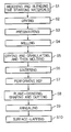
- FIG. 1 shows a flow diagram schematically illustrating some steps in a preferred embodiment of a manufacturing method of a ferrite substrate for thin-film inductors according to the present invention
- FIGS. 2 a to 2 j show perspective views for explanation of a wafer process to produce a thin-film common mode filter array
- FIGS. 3 a to 3 j show perspective views for explanation of a working process to produce the thin-film common mode filter array
- FIG. 4 shows a graph illustrating common mode characteristic of a thin-film common mode filter
- FIG. 5 shows a graph illustrating a relationship among Fe 2 O 3 , NiO and ZnO compositions and permeability ⁇ in the ferrite substrates
- FIG. 6 shows a graph illustrating the measurement results of surface insulation resistance of the ferrite substrates containing various Fe 2 O 3 contents after being sintered
- FIG. 7 shows a graph illustrating the measurement results of surface insulation resistance of the sintered ferrite substrates shown in FIG. 6 after being surface-lapped
- FIG. 8 shows a graph illustrating the measurement results of surface insulation resistance of the ferrite substrates shown in FIG. 7 after being annealed 5 times at a curing temperature of insulating layers (about 400 °C.);
- FIG. 9 shows a graph illustrating the measurement results of surface insulation resistance of the ferrite substrates shown in FIG. 8 after being annealed in vacuum at 1000° C.;
- FIG. 10 shows a graph illustrating the measurement results of surface insulation resistance of the annealed-in-vacuum ferrite substrates shown in FIG. 9 after being surface-lapped with the amount of lapping of 5 ⁇ m or more;
- FIG. 11 shows a graph illustrating the measurement results of the relationship between the amount of lapping and surface resistance of the substrate shown in FIG. 10 ;
- FIG. 12 shows a graph illustrating the measurement results of surface insulation resistance of the surface-lapped ferrite substrates shown in FIG. 10 after being annealed 5 times in vacuum at about 400 ° C.;
- FIG. 13 shows a graph illustrating the measurement results of surface insulation resistance of the ferrite substrates shown in FIG. 12 and NiZn-ferrite substrates produced with addition of Bi 2 O 3 to their basic composition;
- FIG. 14 shows a graph illustrating the measurement results of the relationship between the amount of added Bi 2 O 3 and insulation resistance in the ferrite substrate with Fe 2 O 3 55 molt %;
- FIG. 15 shows a graph illustrating the measurement results of the relationship between the amount of added Bi 2 O 3 and bending strength in the ferrite substrate with Fe 2 O 3 55 mol %;
- FIG. 16 shows a graph illustrating the measurement results of the relationship between bending strength and the amount of added CuO in the NiZn-ferrite substrates produced with addition of CuO to their basic composition
- FIG. 17 shows a graph illustrating the measurement results of the relationship between permeability ⁇ and the amount of added MnO 2 in the substrates produced with addition of MnO 2 to the composition shown in FIG. 16 ;
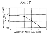
- FIG. 18 shows a graph illustrating the measurement results of the relationship between insulation resistance and the amount of added MnO 2 in the substrates produced with addition of MnO 2 to the composition shown in FIG. 16 ;
- FIG. 19 shows a graph illustrating the measurement results of the relationship between insulation resistance and the amount of added Bi 2 O 3 in the substrates produced by HP and those produced by HIP;
- FIG. 20 shows a graph illustrating the measurement results the relationship between bending strength and the amount of added Bi 2 O 3 in the substrates produced by HP and those produced by HIP;
- FIG. 21 shows a graph illustrating the measurement results of the relationship between applied pressure in HIP and bending strength of the substrates
- FIG. 22 shows a graph illustrating the measurement results the relationship between applied pressure in HP and bending strength of the substrates
- FIG. 23 shows a graph illustrating the measurement results the relationship between density and applied pressure in the ferrite substrates produced by HP and the ferrite substrates produced by HIP, both of which consist basically of Fe 2 O 3 , NiO and ZnO;
- FIG. 24 shows a graph illustrating the measurement results of the relationship between surface roughness and grit number of the used abrasive grain, in the ferrite substrates produced by HP and the ferrite substrates produced by HIP, both of which consist basically of Fe 2 O 3 , NiO and ZnO;
- FIG. 25 shows an optical microscope photograph of the surface of the ferrite substrate that was produced by HIP
- FIG. 26 shows an optical microscope photograph of the surface of the ferrite substrate that was produced by HP.
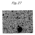
- FIG. 27 shows an optical microscope photograph of the surface of the ferrite substrate that was produced by sheet manufacturing method.
- FIG. 1 schematically illustrates some steps in a preferred embodiment of a manufacturing method of a ferrite substrate for thin-film inductors according to the present invention. The manufacturing steps of the ferrite substrate will be described in detail with reference to the figure hereafter.
- raw materials are weighed according to the blend table so that obtained ferrite substrates will have a predetermined composition, and then are blended by adding purified water (step S 1 ).
- the predetermined composition is Fe 2 O 3 : 40 to 55 mol %, NiO: 15 to 30 mol %, and ZnO: 20 to 40 mol %.
- step S 2 the obtained blended slurry is dried (step S 2 ), and presintered (step S 3 ).
- the obtained presintered material is milled with purified water (step S 4 ).
- the milling is accompanied by adding 150 to 750 ppm in Bi 2 O 3 . CaCO 3 and such also may be added.
- the obtained milled material is dried and granulated, and then is molded (step S 5 ). Further, it is sintered (step S 6 ), in the atmospheric air as combustion gas at about 1160 ° C.
- step S 7 the sintered article undergoes HIP (step S 7 ) that is performed for about 2 hours under the pressure of about 1000 kg/cm 2 at about 1200 ° C.
- the obtained article is plane-grinded, shaped and cut (step S 8 ).
- step S 9 the cut article is heated or annealed (step S 9 ), in the atmospheric air at about 1000 ° C.
- the surface of the annealed article is lapped with the amount of lapping of at least 5 ⁇ m, by use of abrasive grain of grit number #2000 (step S 10 ).
- raw materials are weighed according to the blend table so that obtained ferrite substrates will have a predetermined composition, and then are blended by adding purified water (step S 1 ).
- the predetermined composition is Fe 2 O 3 : 40 to 55 mol %, NiO: 15 to 30 mol %, ZnO: 20 to 40 mol %, CuO: 5 to 10 mol %, and MnO 2 : 0.5 to 2 mol %.
- step S 2 the obtained blended slurry is dried (step S 2 ), and presintered (step S 3 ).
- the obtained presintered material is milled with purified water (step S 4 ).
- the milling may be accompanied by adding CaCO 3 and such.
- the obtained milled material is dried and granulated, and then is molded (step S 5 ). Further, it is sintered (step S 6 ), in the atmospheric air as combustion gas at about 1160 ° C.
- step S 7 the sintered article undergoes HIP (step S 7 ) that is performed for about 2 hours under the pressure of about 1000 kg/cm 2 at about 1200 ° C.
- the obtained article is plane-grinded, shaped and cut (step S 8 ).
- step S 9 the cut article is heated or annealed (step S 9 ), in the atmospheric at 1000 ° C.
- the surface of the annealed article is lapped with the amount of lapping of at least 5 ⁇ m, by use of abrasive grain #2000 (step S 10 ).
- the obtained substrate By undergoing HIP, after being set into the above-mentioned ferrite composition and sintered, and by being annealed and surface-lapped as mentioned above, the obtained substrate achieves a high surface insulation resistance value of 2 ⁇ 10 10 ⁇ cm or more. Further, there is no change (degradation) in bulk insulation resistance and surface insulation resistance in the substrate after being annealed in the thin film process thereafter. Further, mechanical strength (bending strength) of the substrate is enhanced to the value at least 1.5 times larger than that of substrate produced by conventional hot forming press method, which is enough strength for the substrate to undergo the thin film process. Furthermore, the substrate surface becomes densified with almost no voids, as well as the surface in the production process.
- FIGS. 2 a to 2 j and FIGS. 3 a to 3 j show perspective views for explanation of the wafer process and the working process to produce a thin film common mode filter array that consists of two coupled thin film common mode filters, fabricated from the above-mentioned ferrite substrate.
- FIGS. 2 a - 2 j and FIGS. 3 a - 3 j the lower parts of the view show a wafer, and the upper parts show individual chips that are not actually cut to separate.
- the manufacturing process of the thin film common mode filter array will be detailed by these figures hereafter.
- a ferrite wafer that was fabricated by the manufacturing method of FIG. 1 is prepared, and, as shown in FIG. 2 b , a first insulating layer 21 , made of such as polyimide resin, is coated on the wafer 20 , and is then patterned.
- first leads and electrodes of a copper layer 22 are formed on the first insulating layer 21 .
- a second insulating layer 23 made of such as polyimide resin, is coated thereon, and patterned.
- first coils of a copper layer 24 are formed on the second insulating layer 23 .
- a third insulating layer 25 made of such as polyimide resin, is coated thereon, and patterned.
- FIG. 2 g second coils of a copper layer 26 are formed on the third insulating layer 25 .
- a fourth insulating layer 27 made of such as polyimide resin, is coated thereon, and patterned.
- FIG. 2 i second leads of a copper layer 28 are formed on the fourth insulating layer 27 .
- a fifth insulating layer 29 made of such as polyimide resin, is coated thereon, and patterned.
- a silver paste 30 is screen-printed on the leads.
- a ferrite paste 31 for flux return portion is embedded in the core portions.
- a ferrite plate cover 32 is bonded on the processed wafer with adhesive.
- the obtained wafer is cut into bars 33 on each of which a plurality of thin film common mode filter array chips are aligned.
- a mark 34 is printed on the upper side of each of the thin film common mode filter array chips in the bar 33 .
- electrode terminals 35 of Nickel are formed by sputtering on the side of each of the thin film common mode filter array chips in the bar 33 .
- each bar is cut to separate into individual chips 36 .
- the electrode terminals 35 are formed into bilayer structure 37 of a Nickel layer and a tin layer by barrel plating.
- the obtained thin film common mode filter array chips 36 are bonded on a tape 38 .
- the ferrite substrate is required to have high electrical insulation performance in bulk because, as shown in FIG. 3 g , the thin film common mode filter and thin film common mode filter array have the electrode terminals formed on the cut surface of the ferrite substrate. And the ferrite substrate is also required to have high surface insulation performance.
- the thin film common mode filter produced from the substrates is required to have insulation resistance on the order of 10 8 ⁇ between the coil terminals. Although there is no perfect proportionality relation between the substrate surface resistance and actual terminal-to-terminal resistance, the substrate is required to have 2 ⁇ 10 10 ⁇ or more of the combined resistance of the bulk resistance and the surface resistance, to guarantee at least 10 8 ⁇ of the insulation resistance.
- the ferrite substrate is also required to maintain stably high surface insulation performance during such a heat process that is performed in the atmospheric air or Nitrogen gas at more or less 400 ° C. for heat cure of the insulating layer in the wafer process for forming the thin film common mode filter.
- the ferrite substrate is required not to be cracked or so by mechanical shock or thermal shock in the wafer process because, as shown in FIGS. 2 a - 2 j , the thin film common mode filter and thin film common mode filter array are formed all together on the ferrite substrate.
- the resistance to such a crack depends on the bending strength of the substrate, therefore the ferrite substrate is required to have higher bending strength. Particularly, the larger is the size of the substrate, the higher bending strength the substrate must have, to enhance its resistance to crack.
- thin film micropatterns are formed on the ferrite substrate in the production process of the thin film common mode filter and thin film common mode filter array, therefore the coated film on the substrate is required not to billow, and the micropatterns are required not to be deformed, due to rough surface of the substrate or so.
- smaller degree of surface roughness of the substrate than the thickness of the coated film is required for carrying out the thin film process.
- Rmax surface roughness
- FIG. 4 shows a graph illustrating common mode characteristic of a thin film common mode filter fabricated by the above-mentioned process, that is, frequency dependence of intrinsic impedance Z.
- the common mode filters using the substrates made of ferrite materials with various permeability ⁇ about 100 to 1400, acquire almost the same common mode characteristic.
- FIG. 5 shows a graph illustrating the relationship among Fe 2 O 3 , NiO and ZnO compositions and permeability ⁇ in the ferrite substrates.
- the ferrite substrate is required to contain a composition in the range of Fe 2 O 3 : 40 to 70 molt %, NiO: 5 to 35 molt %, ZnO: 10 to 40 mol %.
- FIG. 6 shows a graph illustrating the measurement results of surface insulation resistance of the ferrite substrates just after being sintered, which contain various Fe 2 O 3 contents.
- FIG. 7 shows a graph illustrating the measurement results of surface insulation resistance of the sintered ferrite substrates after being surface-lapped.
- the NiZn ferrite substrates just after being sintered indicate greatly high surface insulation resistance of 10 12 ⁇ or more in the Fe 2 O 3 content range from 30 to 65 mol %. Further, the sintered substrates after being surface-lapped maintain greatly high surface insulation resistance.
- FIG. 8 shows a graph illustrating the measurement results of surface insulation resistance of the ferrite substrates shown in FIG. 7 , which contain various Fe 2 O 3 contents, after being annealed (5 times) at a curing temperature of insulating layers (about 400 ° C.).
- FIG. 9 shows a graph illustrating the measurement results of surface insulation resistance of these ferrite substrates after being annealed in vacuum at 1000 ° C.
- the substrates annealed repeatedly at the curing temperature of insulating layer show degraded surface insulation performance down to the order of 10 9 ⁇ in surface insulation resistance. Further, as understood from FIG. 9 , the substrates annealed in vacuum show greatly degraded surface insulation performance down to the order of 10 8 ⁇ in surface insulation resistance.
- FIG. 10 shows a graph illustrating the measurement results of surface insulation resistance of the annealed-in-vacuum ferrite substrates shown in FIG. 9 after being surface-lapped with the amount of 5 ⁇ m or more.
- the substrates reacquire greatly high surface insulation resistance by being surface-lapped. From this fact, understood is that the decrease in resistance is associated with the surface condition of the ferrite substrate.
- FIG. 11 shows a graph illustrating the measurement results of the relationship between the amount of lapping and surface resistance.
- the amount of surface lapping is set at 5 ⁇ m or more.
- FIG. 12 shows a graph illustrating the measurement results of surface insulation resistance of the surface-lapped ferrite substrates shown in FIG. 10 after being annealed 5 times in vacuum at a curing temperature of insulating layers (about 400 ° C).
- the ferrite substrates annealed for curing insulating layers show smaller decrease in surface resistance.
- the substrates indicate high surface resistance values of 10 10 ⁇ or more in the Fe 2 O 3 content range of 55 mol % or less. The insulation resistance is dropped sharply over the Fe 2 O 3 content range.
- the substrate should have a Fe 2 O 3 content of 55 mol % or less. Further, according to the measurement results of permeability ⁇ shown in FIG. 5 , more preferable is that the substrates have a composition of Fe 2 O 3 : 40 to 55 mol %, NiO: 15 to 30 mol %, ZnO: 20 to 40 mol %.
- FIG. 13 shows a graph illustrating the measurement results of surface insulation resistance of the ferrite substrates shown in FIG. 12 and NiZn-ferrite substrates produced with addition of Bi 2 O 3 to their basic composition of Fe 2 O 3, NiO and ZnO.
- Line a corresponds to the Bi 2 O 3 -added substrates
- line b corresponds to the no-Bi 2 O 3 -added substrates, both of which were annealed in vacuum at 1000° C. and then were surface-lapped with the amount of 8 ⁇ m.
- FIG. 14 shows a graph illustrating the measurement results of the relationship between the amount of added Bi 2 O 3 and insulation resistance in the ferrite substrate with Fe 2 O 3 content of 55 mol %.
- FIG. 15 shows a graph illustrating the measurement results of the relationship between the amount of added Bi 2 O 3 and bending strength in the ferrite substrate with Fe 2 O 3 content of 55 mol %.
- the measurement was based on JIS transverse test.
- the span of the measuring object was 1.4 mm, and the weighing rate was 30 mm/min.
- the insulation resistance and the bending strength are optimized together by adding 150 to 750 ppm of Bi 2 O 3 as the first example of the substrate composition.
- FIG. 16 shows a graph illustrating the measurement results of the relationship between bending strength and the amount of added CuO in the NiZn-ferrite substrates produced with addition of CuO to their basic composition of Fe 2 O 3 , NiO and ZnO.
- FIG. 17 shows a graph illustrating the measurement results of the relationship between permeability ⁇ and the amount of added MnO 2 in the substrates produced with addition of MnO 2 to the composition shown in FIG. 16 .
- FIG. 18 shows a graph illustrating the measurement results of the relationship between insulation resistance and the amount of added MnO 2 in the substrates produced with addition of MnO 2 to the composition shown in FIG. 16 .
- the permeability ⁇ increases with the amount of added MnO 2 from 0.5 to 5 mol %.
- the substrate insulation resistance falls sharply by adding 2 mol % or more of MnO 2, as shown in FIG. 18 .
- the bending strength and the permeability ⁇ can be improved together without the insulation resistance decrease, by adding 5 to 10 mol % of CuO and 0.5 to 2 mol % of MnO 2 as the second example of the substrate composition.
- FIG. 19 shows a graph illustrating the measurement results of the relationship between insulation resistance and the amount of added Bi 2 O 3 , in the ferrite substrates produced by conventional hot forming press method (HP) and the ferrite substrates produced by HIP according to the invention.
- FIG. 20 shows a graph illustrating the measurement results of the relationship between bending strength and the amount of added Bi 2 O3, in the ferrite substrates produced by HP and the ferrite substrates produced by HIP.
- the bending strength of the substrate produced by HIP is about time and a half larger than that of the substrate produced by HP. That is, the substrate produced by HIP is harder to crack. The tendency becomes marked as the wafer size becomes larger.
- FIG. 21 shows a graph illustrating the measurement results of the relationship between applied pressure in HIP and bending strength of the substrates.
- FIG. 22 shows a graph illustrating the measurement results of the relationship between applied pressure in HP and bending strength of the substrates.
- the processing temperature in both HP and HIP was 1200 ° C.
- the substrates acquire large bending strengths by undergoing HIP under the HIP pressure of 0.5t/cm 2 or more.
- the substrate cannot acquire so large bending strengths by undergoing HP under the increased HP pressure, as shown in FIG. 22 .
- Table 1 illustrates the observation results of crack occurrence frequency in the 3-inch and 6-inch ferrite substrates (with thickness of 2mm) produced by HP and the 3-inch and 6-inch ferrite substrates produced by HIP, both of which repeatedly underwent 10 times thermal shocks at 110° C. and 10 times sets of suction and detaching in the carrying process. The number of sample was 20.
- the 3-inch substrates produced by HIP show less crack occurrence frequency than those produced by HP. In the 6-inch substrates, there is a larger difference of the frequency between the substrates by HP and those by HIP.
- TABLE 1 1st 2nd 3rd 4th 5th 6th 7th 8th 9th 10th 3- HP 0 0 1 1 1 2 2 2 2 2 inch HIP 0 0 0 0 0 0 0 0 0 wafer 6- HP 1 4 6 6 8 9 12 15 18 19 inch HIP 0 0 0 0 0 0 0 0 0 1 wafer
- FIG. 23 shows a graph illustrating the measurement results of the relationship between density and applied pressure in the ferrite substrates produced by HP and the ferrite substrates produced by HIP, both of which consist basically of Fe 2 O 3 , NiO and ZnO.
- the substrate density is improved by applying HIP to the substrate.
- FIG. 24 shows a graph illustrating the measurement results of the relationship between surface roughness and grit number of the used abrasive grain, in the ferrite substrates produced by HP and the ferrite substrates produced by HIP, both of which consist basically of Fe 2 O 3 , NiO and ZnO.
- the crystalline grain size of both ferrite substrates was 5 ⁇ m, and #2000 SiC was used as abrasive grain for lapping of both substrates.
- FIG. 25 shows an optical microscope photograph (x 220 ) of the surface of the substrate that was processed by HIP and was lapped with #6000 diamond
- FIG. 26 shows an optical microscope photograph (x 220 ) of the surface of the substrate that was processed by HP and lapped with #6000 diamond
- FIG. 27 shows an optical microscope photograph (x 220 ) of the surface of the substrate that was processed by sheet manufacturing method and was lapped with #6000 diamond.
- the crystalline grain sizes of all the ferrite substrates were 5-6 ⁇ m.
- the surface of the ferrite substrate produced by HIP as shown in FIG. 25 has almost no pin holes, whereas the surface of the ferrite substrate produced by conventional HP as shown in FIG. 26 or produced by HP after sheet manufacturing has some voids. Further, the surface of the ferrite substrate produced by sheet manufacturing method as shown in FIG. 27 has some large vacancies from which the ferrite particles were detached.
Landscapes
- Chemical & Material Sciences (AREA)
- Engineering & Computer Science (AREA)
- Ceramic Engineering (AREA)
- Manufacturing & Machinery (AREA)
- Materials Engineering (AREA)
- Structural Engineering (AREA)
- Organic Chemistry (AREA)
- Inorganic Chemistry (AREA)
- Soft Magnetic Materials (AREA)
- Magnetic Ceramics (AREA)
- Coils Or Transformers For Communication (AREA)
Abstract
Description
- This application is a divisional application of Application Ser. No. 10/862,533, filed Jun. 8, 2004.
- This application claims priority from Japanese patent application No.2003-163563, filed on Jun. 9, 2003, which is incorporated herein by reference.
- 1. Field of the Invention
- The present invention relates to a ferrite substrate for thin-film inductors, to a thin-film common mode filter using the substrate, to a thin-film common mode filter array using the substrate, and to a manufacturing method of the substrate.
- 2. Description of the Related Art
- Common mode filter is a device for suppressing common mode currents that cause electromagnetic interference in parallel transmission lines. The common mode filter has magnetically coupled inductors to remove in-phase noise component.
- Thin-film common mode filter miniaturized and highly integrated by forming bilayered thin-film coils between ferrite substrates and by constructing in chip form, and thin film common mode filter array on which a plurality of the filters are mounted, are described in for example, Japanese Patent Publications Nos. 08-203737A and 11-054326A.
- Generally, such a ferrite substrate is produced by hot forming press method where a hot-pressed block is cut out into substrates with a desired shape and the substrates are then lapped and formed, or by sheet manufacturing method where sheeted ferrites are stacked and pressed with heat and the stacked ferrite is then lapped and formed into a desired shape.
- In the thin-film common mode filter, coils are disposed closely to each other in order to satisfy it's characteristic request and high voltage is applied to these coils. Thus, such filter is required to have high withstand voltage and high reliability in electrical isolation. Also, required is that terminals of the filter should be electrically isolated with each other and formed finely without causing electrical isolation failure between coils. Furthermore, the filter should have miniaturized coils and ferrite substrates with a permeability of about 100-400 in order to be operable at a high frequency (several GHz) band.
- Conventional ferrite substrate for the thin-film common mode filter, however, has a porous crystalline structure with voids and such on its surface, which causes low insulation resistance on its surface and large surface-degradation. The ferrite substrate, therefore, has too poor mechanical strength to undergo thin-film process, and moreover, it has been difficult to form precisely the terminals on the substrate surface.
- It is therefore an object of the present invention to provide a ferrite substrate for thin-film inductors, with a higher surface insulation resistance and less surface-degradation, a thin-film common mode filter using the substrate, a thin-film common mode filter array using the substrate, and a manufacturing method of the substrate.
- Another object of the present invention is to provide a ferrite substrate for thin-film inductors with a high mechanical strength, a thin-film common mode filter using the substrate, a thin-film common mode filter array using the substrate, and a manufacturing method of the substrate.
- A further object of the present invention is to provide a ferrite substrate for thin-film inductors, on a surface of which terminals can be precisely formed without difficulty, a thin-film common mode filter using the substrate, a thin-film common mode filter array using the substrate, and a manufacturing method of the substrate.
- According to the present invention, a ferrite substrate for thin-film inductors is provided, which contains a ferrite composition of di-iron trioxide (Fe2O3): 40 to 55 molt %, nickel oxide (NiO): 5 to 35 molt %, zinc oxide (ZnO): 10 to 40 molt %, and bismuth trioxide (Bi2O3): 150 to 750 ppm, or of Fe2O3:40 to 55 molt %, NiO: 5 to 35 molt %, ZnO: 10 to 40 molt %, cupric oxide (CuO): 5 to 10 molt %, and manganese dioxide (MnO2): 0.5 to 2 molt %, and which has a densified crystalline structure developed by hot isostatic pressing (HIP). Also, a thin-film common mode filter and a thin-film common mode filter array, which are produced from a part of the substrate, are provided.
- More preferably, the substrate contains a ferrite composition of Fe2O3: 40 to 55 mol %, NiO: 15 to 30 mol %, ZnO: 20 to 40 mol %, and Bi2O3: 150 to 750 ppm, or of Fe2O3: 40 to 55 mol %, NiO: 15 to 30 mol %, ZnO: 20 to 40 mol %, CuO: 5 to 10 mol %, and MnO2: 0.5 to 2 mol %.
- By being given the crystalline structure densified by HIP with the above-mentioned ferrite composition, the substrate achieves high surface insulation resistance of 2×10¹⁰ Ω·cm or more, and the common mode filter produced from the substrate can acquire enough electrical isolation between the coils. And, there is no change (degradation) in bulk insulation resistance and surface insulation resistance of the substrate after being annealed in the thin film process. Further, mechanical strength (bending strength) of the substrate is enhanced to the value at least 1.5 times larger than that of substrate produced by conventional hot forming press method, which is a enough strength for the substrate to undergo the thin film process. Furthermore, the densified substrate-surface with almost no voids can prevent electrical trouble due to plating on unwanted portion when the terminals and the like are formed by plating. In addition, the terminal patterns are able to being formed precisely because of the densified substrate-surface.
- Preferably, the substrate is a wafer with diameter of 3 inches or more.
- According to the present invention, a manufacturing method of a ferrite substrate for thin film inductors is, further provided, which includes a step of blending, and adding if needed, raw materials to meet a composition of Fe2O3: 40 to 55 mol %, NiO: 5 to 35 mol %, ZnO: 10 to 40 mol %, and Bi2O3: 150 to 750 ppm, or of Fe2O3: 40 to 55 mol %, NiO: 5 to 35 mol %, ZnO: 10 to 40 mol %, CuO: 5 to 10 mol %, and MnO2: 0.5 to 2 mol %, and a step of molding and sintering the blended material, and then applying HIP to the sintered article.
- More preferably, the method includes a step of blending raw materials to meet a composition of Fe2O3: 40 to 55 mol %, NiO: 15 to 30 mol %, ZnO: 20 to 40 mol %, and Bi2O3: 150 to 750 ppm, or of Fe2O3: 40 to 55 mol %, NiO: 15 to 30 mol %, ZnO: 20 to 40 mol %, CuO: 5 to 10 mol %, and MnO2: 0.5 to 2 mol %.
- By undergoing HIP, after being set into the above-mentioned ferrite composition and sintered, the obtained substrate achieves a high surface insulation resistance value of 2×10¹⁰ Ω·cm or more, and the common mode filter produced from the substrate can acquire enough electrical isolation between the coils. Further, there is no change or degradation in bulk insulation resistance and surface insulation resistance of the substrate after being annealed in the thin film process. Further, mechanical strength or bending strength of the substrate is enhanced to the value at least 1.5 times larger than that of substrate produced by conventional hot forming press method, which is a enough strength for the substrate to undergo the thin film process. Furthermore, the densified substrate-surface with almost no voids can prevent electrical trouble due to plating on unwanted portion when the terminals and like are formed by plating. In addition, the terminal patterns are able to being formed precisely because of the densified substrate-surface.
- Preferably, the method further includes a step of annealing the obtained article and surface-lapping the annealed article with the amount of lapping at least 5 μm after applying HIP to the article.
- Further objects and advantages of the present invention will be apparent from the following description of the preferred embodiments of the invention as illustrated in the accompanying drawings.
-
FIG. 1 shows a flow diagram schematically illustrating some steps in a preferred embodiment of a manufacturing method of a ferrite substrate for thin-film inductors according to the present invention; -
FIGS. 2 a to 2 j show perspective views for explanation of a wafer process to produce a thin-film common mode filter array; -
FIGS. 3 a to 3 j show perspective views for explanation of a working process to produce the thin-film common mode filter array; -
FIG. 4 shows a graph illustrating common mode characteristic of a thin-film common mode filter; -
FIG. 5 shows a graph illustrating a relationship among Fe2O3, NiO and ZnO compositions and permeability μ in the ferrite substrates; -
FIG. 6 shows a graph illustrating the measurement results of surface insulation resistance of the ferrite substrates containing various Fe2O3 contents after being sintered; -
FIG. 7 shows a graph illustrating the measurement results of surface insulation resistance of the sintered ferrite substrates shown inFIG. 6 after being surface-lapped; -
FIG. 8 shows a graph illustrating the measurement results of surface insulation resistance of the ferrite substrates shown inFIG. 7 after being annealed 5 times at a curing temperature of insulating layers (about 400 °C.); -
FIG. 9 shows a graph illustrating the measurement results of surface insulation resistance of the ferrite substrates shown inFIG. 8 after being annealed in vacuum at 1000° C.; -
FIG. 10 shows a graph illustrating the measurement results of surface insulation resistance of the annealed-in-vacuum ferrite substrates shown inFIG. 9 after being surface-lapped with the amount of lapping of 5 μm or more; -
FIG. 11 shows a graph illustrating the measurement results of the relationship between the amount of lapping and surface resistance of the substrate shown inFIG. 10 ; -
FIG. 12 shows a graph illustrating the measurement results of surface insulation resistance of the surface-lapped ferrite substrates shown inFIG. 10 after being annealed 5 times in vacuum at about 400 ° C.; -
FIG. 13 shows a graph illustrating the measurement results of surface insulation resistance of the ferrite substrates shown inFIG. 12 and NiZn-ferrite substrates produced with addition of Bi2O3 to their basic composition; -
FIG. 14 shows a graph illustrating the measurement results of the relationship between the amount of added Bi2O3 and insulation resistance in the ferrite substrate with Fe2O3 55 molt %; -
FIG. 15 shows a graph illustrating the measurement results of the relationship between the amount of added Bi2O3 and bending strength in the ferrite substrate with Fe2O3 55 mol %; -
FIG. 16 shows a graph illustrating the measurement results of the relationship between bending strength and the amount of added CuO in the NiZn-ferrite substrates produced with addition of CuO to their basic composition; -
FIG. 17 shows a graph illustrating the measurement results of the relationship between permeability μ and the amount of added MnO2 in the substrates produced with addition of MnO2 to the composition shown inFIG. 16 ; -
FIG. 18 shows a graph illustrating the measurement results of the relationship between insulation resistance and the amount of added MnO2 in the substrates produced with addition of MnO2 to the composition shown inFIG. 16 ; -
FIG. 19 shows a graph illustrating the measurement results of the relationship between insulation resistance and the amount of added Bi2O3 in the substrates produced by HP and those produced by HIP; -
FIG. 20 shows a graph illustrating the measurement results the relationship between bending strength and the amount of added Bi2O3 in the substrates produced by HP and those produced by HIP; -
FIG. 21 shows a graph illustrating the measurement results of the relationship between applied pressure in HIP and bending strength of the substrates; -
FIG. 22 shows a graph illustrating the measurement results the relationship between applied pressure in HP and bending strength of the substrates; -
FIG. 23 shows a graph illustrating the measurement results the relationship between density and applied pressure in the ferrite substrates produced by HP and the ferrite substrates produced by HIP, both of which consist basically of Fe2O3, NiO and ZnO; -
FIG. 24 shows a graph illustrating the measurement results of the relationship between surface roughness and grit number of the used abrasive grain, in the ferrite substrates produced by HP and the ferrite substrates produced by HIP, both of which consist basically of Fe2O3, NiO and ZnO; -
FIG. 25 shows an optical microscope photograph of the surface of the ferrite substrate that was produced by HIP; -
FIG. 26 shows an optical microscope photograph of the surface of the ferrite substrate that was produced by HP; and -
FIG. 27 shows an optical microscope photograph of the surface of the ferrite substrate that was produced by sheet manufacturing method. -
FIG. 1 schematically illustrates some steps in a preferred embodiment of a manufacturing method of a ferrite substrate for thin-film inductors according to the present invention. The manufacturing steps of the ferrite substrate will be described in detail with reference to the figure hereafter. - First example of the substrate composition
- First, raw materials are weighed according to the blend table so that obtained ferrite substrates will have a predetermined composition, and then are blended by adding purified water (step S1). The predetermined composition is Fe2O3: 40 to 55 mol %, NiO: 15 to 30 mol %, and ZnO: 20 to 40 mol %.
- Next, the obtained blended slurry is dried (step S2), and presintered (step S3).
- Then, the obtained presintered material is milled with purified water (step S4). The milling is accompanied by adding 150 to 750 ppm in Bi2O3. CaCO3 and such also may be added.
- Next, the obtained milled material is dried and granulated, and then is molded (step S5). Further, it is sintered (step S6), in the atmospheric air as combustion gas at about 1160 ° C.
- Then, the sintered article undergoes HIP (step S7) that is performed for about 2 hours under the pressure of about 1000 kg/cm2 at about 1200 ° C.
- Then, the obtained article is plane-grinded, shaped and cut (step S8).
- Thereafter, the cut article is heated or annealed (step S9), in the atmospheric air at about 1000 ° C.
- Then, the surface of the annealed article is lapped with the amount of lapping of at least 5 μm, by use of abrasive grain of grit number #2000 (step S10).
- Second example of the substrate composition
- First, raw materials are weighed according to the blend table so that obtained ferrite substrates will have a predetermined composition, and then are blended by adding purified water (step S1). The predetermined composition is Fe2O3: 40 to 55 mol %, NiO: 15 to 30 mol %, ZnO: 20 to 40 mol %, CuO: 5 to 10 mol %, and MnO2: 0.5 to 2 mol %.
- Next, the obtained blended slurry is dried (step S2), and presintered (step S3).
- Then, the obtained presintered material is milled with purified water (step S4). The milling may be accompanied by adding CaCO3 and such.
- Next, the obtained milled material is dried and granulated, and then is molded (step S5). Further, it is sintered (step S6), in the atmospheric air as combustion gas at about 1160 ° C.
- Then, the sintered article undergoes HIP (step S7) that is performed for about 2 hours under the pressure of about 1000 kg/cm2 at about 1200 ° C.
- Then, the obtained article is plane-grinded, shaped and cut (step S8).
- Thereafter, the cut article is heated or annealed (step S9), in the atmospheric at 1000 ° C.
- Then, the surface of the annealed article is lapped with the amount of lapping of at least 5 μm, by use of abrasive grain #2000 (step S10).
- By undergoing HIP, after being set into the above-mentioned ferrite composition and sintered, and by being annealed and surface-lapped as mentioned above, the obtained substrate achieves a high surface insulation resistance value of 2×10¹⁰ Ω·cm or more. Further, there is no change (degradation) in bulk insulation resistance and surface insulation resistance in the substrate after being annealed in the thin film process thereafter. Further, mechanical strength (bending strength) of the substrate is enhanced to the value at least 1.5 times larger than that of substrate produced by conventional hot forming press method, which is enough strength for the substrate to undergo the thin film process. Furthermore, the substrate surface becomes densified with almost no voids, as well as the surface in the production process.
-
FIGS. 2 a to 2 j andFIGS. 3 a to 3 j show perspective views for explanation of the wafer process and the working process to produce a thin film common mode filter array that consists of two coupled thin film common mode filters, fabricated from the above-mentioned ferrite substrate. InFIGS. 2 a-2 j andFIGS. 3 a-3 j, the lower parts of the view show a wafer, and the upper parts show individual chips that are not actually cut to separate. The manufacturing process of the thin film common mode filter array will be detailed by these figures hereafter. - First, as shown in
FIG. 2 a, a ferrite wafer that was fabricated by the manufacturing method ofFIG. 1 is prepared, and, as shown inFIG. 2 b, a first insulatinglayer 21, made of such as polyimide resin, is coated on thewafer 20, and is then patterned. - Next, as shown in
FIG. 2 c, first leads and electrodes of acopper layer 22 are formed on the first insulatinglayer 21. Then, as shown inFIG. 2 d, a second insulatinglayer 23, made of such as polyimide resin, is coated thereon, and patterned. - Then, as shown in
FIG. 2 e, first coils of acopper layer 24 are formed on the second insulatinglayer 23. Then, as shown inFIG. 2 f, a third insulatinglayer 25, made of such as polyimide resin, is coated thereon, and patterned. - Then, as shown in
FIG. 2 g, second coils of acopper layer 26 are formed on the third insulatinglayer 25. Then, as shown inFIG. 2 h, a fourth insulatinglayer 27, made of such as polyimide resin, is coated thereon, and patterned. - Then, as shown in
FIG. 2 i, second leads of acopper layer 28 are formed on the fourth insulatinglayer 27. Then, as shown inFIGS. 2 j and 3 a, a fifth insulatinglayer 29, made of such as polyimide resin, is coated thereon, and patterned. - After that, as shown in
FIG. 3 b, asilver paste 30 is screen-printed on the leads. Then, as shown inFIG. 3 c, aferrite paste 31 for flux return portion is embedded in the core portions. - Then, as shown in
FIG. 3 d, aferrite plate cover 32 is bonded on the processed wafer with adhesive. - Then, as shown in
FIG. 3 e, the obtained wafer is cut intobars 33 on each of which a plurality of thin film common mode filter array chips are aligned. - Then, as shown in
FIG. 3 f, amark 34 is printed on the upper side of each of the thin film common mode filter array chips in thebar 33. Then, as shown inFIG. 3 g,electrode terminals 35 of Nickel are formed by sputtering on the side of each of the thin film common mode filter array chips in thebar 33. - After that, as shown in
FIG. 3 h, each bar is cut to separate intoindividual chips 36. Then, as shown inFIG. 3 i, theelectrode terminals 35 are formed intobilayer structure 37 of a Nickel layer and a tin layer by barrel plating. Further, as shown inFIG. 3 j, the obtained thin film common mode filter array chips 36 are bonded on atape 38. - The ferrite substrate is required to have high electrical insulation performance in bulk because, as shown in
FIG. 3 g, the thin film common mode filter and thin film common mode filter array have the electrode terminals formed on the cut surface of the ferrite substrate. And the ferrite substrate is also required to have high surface insulation performance. The thin film common mode filter produced from the substrates is required to have insulation resistance on the order of 108 Ω between the coil terminals. Although there is no perfect proportionality relation between the substrate surface resistance and actual terminal-to-terminal resistance, the substrate is required to have 2×10¹⁰ Ω or more of the combined resistance of the bulk resistance and the surface resistance, to guarantee at least 108 Ω of the insulation resistance. Furthermore, the ferrite substrate is also required to maintain stably high surface insulation performance during such a heat process that is performed in the atmospheric air or Nitrogen gas at more or less 400 ° C. for heat cure of the insulating layer in the wafer process for forming the thin film common mode filter. - In addition, the ferrite substrate is required not to be cracked or so by mechanical shock or thermal shock in the wafer process because, as shown in
FIGS. 2 a-2 j, the thin film common mode filter and thin film common mode filter array are formed all together on the ferrite substrate. The resistance to such a crack depends on the bending strength of the substrate, therefore the ferrite substrate is required to have higher bending strength. Particularly, the larger is the size of the substrate, the higher bending strength the substrate must have, to enhance its resistance to crack. - Further, as mentioned above, thin film micropatterns are formed on the ferrite substrate in the production process of the thin film common mode filter and thin film common mode filter array, therefore the coated film on the substrate is required not to billow, and the micropatterns are required not to be deformed, due to rough surface of the substrate or so. Usually, smaller degree of surface roughness of the substrate than the thickness of the coated film is required for carrying out the thin film process. For example, in the process of coating the polyimide films, patterning is difficult to be performed on the substrate with surface roughness Rmax of 6 μm or more.
-
FIG. 4 shows a graph illustrating common mode characteristic of a thin film common mode filter fabricated by the above-mentioned process, that is, frequency dependence of intrinsic impedance Z. - As understood from
FIG. 4 , the common mode filters, using the substrates made of ferrite materials with various permeability μ about 100 to 1400, acquire almost the same common mode characteristic. -
FIG. 5 shows a graph illustrating the relationship among Fe2O3, NiO and ZnO compositions and permeability μ in the ferrite substrates. - As clarified from in
FIG. 5 , to meet the common mode impedance characteristic of the thin film common mode filter shown inFIG. 4 , the ferrite substrate is required to contain a composition in the range of Fe2O3: 40 to 70 molt %, NiO: 5 to 35 molt %, ZnO: 10 to 40 mol %. -
FIG. 6 shows a graph illustrating the measurement results of surface insulation resistance of the ferrite substrates just after being sintered, which contain various Fe2O3 contents. AndFIG. 7 shows a graph illustrating the measurement results of surface insulation resistance of the sintered ferrite substrates after being surface-lapped. - As understood from
FIG. 6 , the NiZn ferrite substrates just after being sintered indicate greatly high surface insulation resistance of 1012 Ω or more in the Fe2O3 content range from 30 to 65 mol %. Further, the sintered substrates after being surface-lapped maintain greatly high surface insulation resistance. -
FIG. 8 shows a graph illustrating the measurement results of surface insulation resistance of the ferrite substrates shown inFIG. 7 , which contain various Fe2O3 contents, after being annealed (5 times) at a curing temperature of insulating layers (about 400 ° C.). AndFIG. 9 shows a graph illustrating the measurement results of surface insulation resistance of these ferrite substrates after being annealed in vacuum at 1000 ° C. - As understood from
FIG. 8 , the substrates annealed repeatedly at the curing temperature of insulating layer show degraded surface insulation performance down to the order of 109 Ω in surface insulation resistance. Further, as understood fromFIG. 9 , the substrates annealed in vacuum show greatly degraded surface insulation performance down to the order of 108 Ω in surface insulation resistance. -
FIG. 10 shows a graph illustrating the measurement results of surface insulation resistance of the annealed-in-vacuum ferrite substrates shown inFIG. 9 after being surface-lapped with the amount of 5 μm or more. - From
FIG. 10 , it is noticed that the substrates reacquire greatly high surface insulation resistance by being surface-lapped. From this fact, understood is that the decrease in resistance is associated with the surface condition of the ferrite substrate. -
FIG. 11 shows a graph illustrating the measurement results of the relationship between the amount of lapping and surface resistance. - From
FIG. 11 , it is noticed that the surface resistance rises sharply over 5 μm of the amount of lapping. Therefore, preferable is that the amount of surface lapping is set at 5 μm or more. -
FIG. 12 shows a graph illustrating the measurement results of surface insulation resistance of the surface-lapped ferrite substrates shown inFIG. 10 after being annealed 5 times in vacuum at a curing temperature of insulating layers (about 400 ° C). - As evidenced by comparing
FIG. 12 withFIG. 8 , by being surface-lapped with the amount of 5 μm or more, the ferrite substrates annealed for curing insulating layers show smaller decrease in surface resistance. Especially, the substrates indicate high surface resistance values of 1010 Ω or more in the Fe2O3 content range of 55 mol % or less. The insulation resistance is dropped sharply over the Fe2O3 content range. - Therefore, to guarantee the resistance of at least 2×10¹⁰ Ω, the substrate should have a Fe2O3 content of 55 mol % or less. Further, according to the measurement results of permeability μ shown in
FIG. 5 , more preferable is that the substrates have a composition of Fe2O3: 40 to 55 mol %, NiO: 15 to 30 mol %, ZnO: 20 to 40 mol %. -
FIG. 13 shows a graph illustrating the measurement results of surface insulation resistance of the ferrite substrates shown inFIG. 12 and NiZn-ferrite substrates produced with addition of Bi2O3 to their basic composition of Fe2O3, NiO and ZnO. Line a corresponds to the Bi2O3-added substrates, and line b corresponds to the no-Bi2O3-added substrates, both of which were annealed in vacuum at 1000° C. and then were surface-lapped with the amount of 8 μm. - It is noted that the surface insulation resistance increases by adding Bi2O3.
-
FIG. 14 shows a graph illustrating the measurement results of the relationship between the amount of added Bi2O3 and insulation resistance in the ferrite substrate with Fe2O3 content of 55 mol %. - From
FIG. 14 , it is noticed that the insulation resistance is greatly improved by adding 150 ppm or more of Bi2O3. -
FIG. 15 shows a graph illustrating the measurement results of the relationship between the amount of added Bi2O3 and bending strength in the ferrite substrate with Fe2O3 content of 55 mol %. The measurement was based on JIS transverse test. The span of the measuring object was 1.4 mm, and the weighing rate was 30 mm/min. - From
FIG. 15 , it is noticed that the bending strength falls sharply by adding 750 ppm or more of Bi2O3. - As mentioned above, understood is that the insulation resistance and the bending strength are optimized together by adding 150 to 750 ppm of Bi2O3 as the first example of the substrate composition.
-
FIG. 16 shows a graph illustrating the measurement results of the relationship between bending strength and the amount of added CuO in the NiZn-ferrite substrates produced with addition of CuO to their basic composition of Fe2O3, NiO and ZnO. - From
FIG. 16 , it is noticed that the bending strength increases with the amount of added CuO from 5 to 10 mol %. -
FIG. 17 shows a graph illustrating the measurement results of the relationship between permeability μ and the amount of added MnO2 in the substrates produced with addition of MnO2 to the composition shown inFIG. 16 . AndFIG. 18 shows a graph illustrating the measurement results of the relationship between insulation resistance and the amount of added MnO2 in the substrates produced with addition of MnO2 to the composition shown inFIG. 16 . - As clarified from
FIG. 17 , the permeability μ increases with the amount of added MnO2 from 0.5 to 5 mol %. However, the substrate insulation resistance falls sharply by adding 2 mol % or more of MnO2, as shown inFIG. 18 . - Therefore, the bending strength and the permeability μ can be improved together without the insulation resistance decrease, by adding 5 to 10 mol % of CuO and 0.5 to 2 mol % of MnO2 as the second example of the substrate composition.
-
FIG. 19 shows a graph illustrating the measurement results of the relationship between insulation resistance and the amount of added Bi2O3, in the ferrite substrates produced by conventional hot forming press method (HP) and the ferrite substrates produced by HIP according to the invention. AndFIG. 20 shows a graph illustrating the measurement results of the relationship between bending strength and the amount of added Bi2O3, in the ferrite substrates produced by HP and the ferrite substrates produced by HIP. - As shown in
FIG. 19 , there is little difference in the insulation resistance between the ferrite substrates produced by HP and those produced by HIP. However, as shown inFIG. 20 , the bending strength of the substrate produced by HIP is about time and a half larger than that of the substrate produced by HP. That is, the substrate produced by HIP is harder to crack. The tendency becomes marked as the wafer size becomes larger. -
FIG. 21 shows a graph illustrating the measurement results of the relationship between applied pressure in HIP and bending strength of the substrates. AndFIG. 22 shows a graph illustrating the measurement results of the relationship between applied pressure in HP and bending strength of the substrates. The processing temperature in both HP and HIP was 1200 ° C. - As shown in
FIG. 21 , it is noticed that the substrates acquire large bending strengths by undergoing HIP under the HIP pressure of 0.5t/cm2 or more. On the other hand, the substrate cannot acquire so large bending strengths by undergoing HP under the increased HP pressure, as shown inFIG. 22 . - Table 1 illustrates the observation results of crack occurrence frequency in the 3-inch and 6-inch ferrite substrates (with thickness of 2mm) produced by HP and the 3-inch and 6-inch ferrite substrates produced by HIP, both of which repeatedly underwent 10 times thermal shocks at 110° C. and 10 times sets of suction and detaching in the carrying process. The number of sample was 20.
- The 3-inch substrates produced by HIP show less crack occurrence frequency than those produced by HP. In the 6-inch substrates, there is a larger difference of the frequency between the substrates by HP and those by HIP.
TABLE 1 1st 2nd 3rd 4th 5th 6th 7th 8th 9th 10th 3- HP 0 0 1 1 1 2 2 2 2 2 inch HIP 0 0 0 0 0 0 0 0 0 0 wafer 6- HP 1 4 6 6 8 9 12 15 18 19 inch HIP 0 0 0 0 0 0 0 0 0 1 wafer -
FIG. 23 shows a graph illustrating the measurement results of the relationship between density and applied pressure in the ferrite substrates produced by HP and the ferrite substrates produced by HIP, both of which consist basically of Fe2O3, NiO and ZnO. - As shown in
FIG. 23 , it is noticed that the substrate density is improved by applying HIP to the substrate. -
FIG. 24 shows a graph illustrating the measurement results of the relationship between surface roughness and grit number of the used abrasive grain, in the ferrite substrates produced by HP and the ferrite substrates produced by HIP, both of which consist basically of Fe2O3, NiO and ZnO. The crystalline grain size of both ferrite substrates was 5 μm, and #2000 SiC was used as abrasive grain for lapping of both substrates. - As shown in
FIG. 24 , it is noticed that the surface roughness decreases greatly by application of HIP to the substrate. Further, the surface roughness of the substrates produced by HP shows less change as the used abrasive grain becomes fine according to the grit number change from #1200 to #2000 and to #4000, whereas the surface roughness of the substrates produced by HIP is improved as the used abrasive grain becomes fine. -
FIG. 25 shows an optical microscope photograph (x220) of the surface of the substrate that was processed by HIP and was lapped with #6000 diamond, andFIG. 26 shows an optical microscope photograph (x220) of the surface of the substrate that was processed by HP and lapped with #6000 diamond. Further,FIG. 27 shows an optical microscope photograph (x220) of the surface of the substrate that was processed by sheet manufacturing method and was lapped with #6000 diamond. The crystalline grain sizes of all the ferrite substrates were 5-6 μm. - The surface of the ferrite substrate produced by HIP as shown in
FIG. 25 has almost no pin holes, whereas the surface of the ferrite substrate produced by conventional HP as shown inFIG. 26 or produced by HP after sheet manufacturing has some voids. Further, the surface of the ferrite substrate produced by sheet manufacturing method as shown inFIG. 27 has some large vacancies from which the ferrite particles were detached. - All the foregoing embodiments are by way of example of the present invention only and not intended to be limiting, and many widely different alternations and modifications of the present invention may be constructed without departing from the spirit and scope of the present invention. Accordingly, the present invention is limited only as defined in the following claims and equivalents thereto.
Claims (9)
Priority Applications (1)
| Application Number | Priority Date | Filing Date | Title |
|---|---|---|---|
| US11/607,065 US7425376B2 (en) | 2003-06-09 | 2006-12-01 | Ferrite substrate for thin-film inductors, thin-film common mode filter using the substrate, and thin-film common mode filter array using the substrate |
Applications Claiming Priority (4)
| Application Number | Priority Date | Filing Date | Title |
|---|---|---|---|
| JP163563/2003 | 2003-06-09 | ||
| JP2003163563A JP4370817B2 (en) | 2003-06-09 | 2003-06-09 | Ferrite substrate manufacturing method |
| US10/862,533 US7387847B2 (en) | 2003-06-09 | 2004-06-08 | Ferrite substrate, thin-film common mode filter using the substrate, thin-film common mode filter array using the substrate and manufacturing method of the substrate |
| US11/607,065 US7425376B2 (en) | 2003-06-09 | 2006-12-01 | Ferrite substrate for thin-film inductors, thin-film common mode filter using the substrate, and thin-film common mode filter array using the substrate |
Related Parent Applications (1)
| Application Number | Title | Priority Date | Filing Date |
|---|---|---|---|
| US10/862,533 Division US7387847B2 (en) | 2003-06-09 | 2004-06-08 | Ferrite substrate, thin-film common mode filter using the substrate, thin-film common mode filter array using the substrate and manufacturing method of the substrate |
Publications (2)
| Publication Number | Publication Date |
|---|---|
| US20070077458A1 true US20070077458A1 (en) | 2007-04-05 |
| US7425376B2 US7425376B2 (en) | 2008-09-16 |
Family
ID=33487576
Family Applications (2)
| Application Number | Title | Priority Date | Filing Date |
|---|---|---|---|
| US10/862,533 Expired - Lifetime US7387847B2 (en) | 2003-06-09 | 2004-06-08 | Ferrite substrate, thin-film common mode filter using the substrate, thin-film common mode filter array using the substrate and manufacturing method of the substrate |
| US11/607,065 Expired - Fee Related US7425376B2 (en) | 2003-06-09 | 2006-12-01 | Ferrite substrate for thin-film inductors, thin-film common mode filter using the substrate, and thin-film common mode filter array using the substrate |
Family Applications Before (1)
| Application Number | Title | Priority Date | Filing Date |
|---|---|---|---|
| US10/862,533 Expired - Lifetime US7387847B2 (en) | 2003-06-09 | 2004-06-08 | Ferrite substrate, thin-film common mode filter using the substrate, thin-film common mode filter array using the substrate and manufacturing method of the substrate |
Country Status (3)
| Country | Link |
|---|---|
| US (2) | US7387847B2 (en) |
| JP (1) | JP4370817B2 (en) |
| CN (1) | CN1574124A (en) |
Cited By (2)
| Publication number | Priority date | Publication date | Assignee | Title |
|---|---|---|---|---|
| US9230722B2 (en) | 2011-09-02 | 2016-01-05 | Murata Manufacturing Co., Ltd. | Ferrite ceramic composition, ceramic electronic component, and process for producing ceramic electronic component |
| US9245680B2 (en) | 2011-09-02 | 2016-01-26 | Murata Manufacturing Co., Ltd. | Common mode choke coil and method for manufacturing the same |
Families Citing this family (15)
| Publication number | Priority date | Publication date | Assignee | Title |
|---|---|---|---|---|
| JP4591689B2 (en) * | 2005-04-28 | 2010-12-01 | Tdk株式会社 | Manufacturing method of LC composite parts |
| JP2007091538A (en) * | 2005-09-29 | 2007-04-12 | Tdk Corp | NONMAGNETIC Zn FERRITE AND COMPOUNDED MULTILAYER ELECTRONIC COMPONENT USING IT |
| EP2187843B1 (en) * | 2007-09-13 | 2015-10-07 | DERU GmbH | Endoprosthesis component |
| JP5535212B2 (en) * | 2008-08-07 | 2014-07-02 | デル・ゲゼルシャフト・ミット・ベシュレンクテル・ハフツング | Manufacturing method of ceramic member |
| US20110127700A1 (en) * | 2008-08-07 | 2011-06-02 | Deru Gmbh | Method for producing a ceramic component |
| US7830236B2 (en) * | 2008-09-09 | 2010-11-09 | Gm Global Technology Operations, Inc. | DC-DC converter for fuel cell application using hybrid inductor core material |
| CN101477869B (en) * | 2008-09-23 | 2011-09-14 | 彭亦瑜 | Novel nickel zincium soft magnetic ferrite and manufacturing process thereof |
| EP2544200B1 (en) * | 2010-03-05 | 2020-08-26 | Murata Manufacturing Co., Ltd. | Ceramic electronic component and method for producing ceramic electronic component |
| WO2012149430A1 (en) * | 2011-04-27 | 2012-11-01 | Todd Shudarek | Combined active and passive harmonic mitigation devices and applications thereof |
| KR101853137B1 (en) * | 2011-12-22 | 2018-05-02 | 삼성전기주식회사 | Coil Parts And Method of Manufacturing The Same |
| KR101771741B1 (en) * | 2012-11-13 | 2017-09-05 | 삼성전기주식회사 | Filter chip elements and method for preparing thereof |
| KR101823267B1 (en) * | 2016-11-01 | 2018-01-29 | 삼성전기주식회사 | Thin film inductor and method of fabricating the same |
| CN108558383B (en) * | 2018-04-04 | 2021-10-15 | 全球能源互联网研究院有限公司 | NiZn ferrite material and preparation method |
| CN111205075B (en) * | 2019-10-23 | 2021-04-20 | 横店集团东磁股份有限公司 | A kind of nickel zinc ferrite material and preparation method thereof |
| CN114300249A (en) * | 2021-12-31 | 2022-04-08 | 安徽龙磁金属科技有限公司 | Manufacturing method of high-power composite molding inductor |
Citations (1)
| Publication number | Priority date | Publication date | Assignee | Title |
|---|---|---|---|---|
| US20040031946A1 (en) * | 2000-12-27 | 2004-02-19 | Masayuki Inagaki | Low-loss magnetic oxide material and method for making |
Family Cites Families (9)
| Publication number | Priority date | Publication date | Assignee | Title |
|---|---|---|---|---|
| JPS56155100A (en) * | 1980-05-02 | 1981-12-01 | Ngk Insulators Ltd | Production of single crystal of ferrite |
| JPS61117805A (en) | 1984-11-14 | 1986-06-05 | Sumitomo Special Metals Co Ltd | Mn-zn system soft ferrite and manufacture thereof |
| JPH0616451B2 (en) | 1986-05-06 | 1994-03-02 | 三菱電機株式会社 | Low loss oxide magnetic material |
| JP3601619B2 (en) | 1995-01-23 | 2004-12-15 | 株式会社村田製作所 | Common mode choke coil |
| JP3615024B2 (en) | 1997-08-04 | 2005-01-26 | 株式会社村田製作所 | Coil parts |
| JP2001244123A (en) * | 2000-02-28 | 2001-09-07 | Kawatetsu Mining Co Ltd | Surface mount type planar magnetic element and method of manufacturing the same |
| DE60136223D1 (en) * | 2001-03-01 | 2008-11-27 | Tdk Corp | SINTERED MAGNETIC OXIDE AND HIGH FREQUENCY CIRCUIT UNIT USING THIS |
| JP2003109814A (en) | 2001-09-28 | 2003-04-11 | Nec Tokin Corp | Oxide magnetic material |
| JP2005535110A (en) * | 2002-06-25 | 2005-11-17 | タイコ・エレクトロニクス・コーポレイション | Integrated devices that provide overcurrent and overvoltage protection and common mode filtering for data bus interfaces |
-
2003
- 2003-06-09 JP JP2003163563A patent/JP4370817B2/en not_active Expired - Fee Related
-
2004
- 2004-06-08 US US10/862,533 patent/US7387847B2/en not_active Expired - Lifetime
- 2004-06-09 CN CNA2004100592301A patent/CN1574124A/en active Pending
-
2006
- 2006-12-01 US US11/607,065 patent/US7425376B2/en not_active Expired - Fee Related
Patent Citations (1)
| Publication number | Priority date | Publication date | Assignee | Title |
|---|---|---|---|---|
| US20040031946A1 (en) * | 2000-12-27 | 2004-02-19 | Masayuki Inagaki | Low-loss magnetic oxide material and method for making |
Cited By (2)
| Publication number | Priority date | Publication date | Assignee | Title |
|---|---|---|---|---|
| US9230722B2 (en) | 2011-09-02 | 2016-01-05 | Murata Manufacturing Co., Ltd. | Ferrite ceramic composition, ceramic electronic component, and process for producing ceramic electronic component |
| US9245680B2 (en) | 2011-09-02 | 2016-01-26 | Murata Manufacturing Co., Ltd. | Common mode choke coil and method for manufacturing the same |
Also Published As
| Publication number | Publication date |
|---|---|
| JP2005001894A (en) | 2005-01-06 |
| US20040246088A1 (en) | 2004-12-09 |
| US7425376B2 (en) | 2008-09-16 |
| CN1574124A (en) | 2005-02-02 |
| US7387847B2 (en) | 2008-06-17 |
| JP4370817B2 (en) | 2009-11-25 |
Similar Documents
| Publication | Publication Date | Title |
|---|---|---|
| US7425376B2 (en) | Ferrite substrate for thin-film inductors, thin-film common mode filter using the substrate, and thin-film common mode filter array using the substrate | |
| CN209962815U (en) | Laminated coil component | |
| USRE45645E1 (en) | Multilayer coil component and method for manufacturing the same | |
| US20100271163A1 (en) | Open magnetic circuit multilayer coil component and process for producing the open magnetic circuit multilayer coil component | |
| KR101181055B1 (en) | Dielectric ceramic composition, complex electronic device and multilayer ceramic capacitor | |
| CN102365249B (en) | Dielectric ceramic composition, multilayer dielectric substrate, electronic component, and method for producing dielectric ceramic composition | |
| EP2722857A1 (en) | Multilayer coil part | |
| US6489877B1 (en) | Ceramic inductor component and composite component using same | |
| EP2549491B1 (en) | Surface mountable negative coefficient characteristic ceramic thermistor based on Mn, Co and Ti | |
| CN112885561B (en) | Coil component | |
| US4956114A (en) | Sintered ferrite body, chip inductor, and composite LC part | |
| KR100361310B1 (en) | Negative Temperature Coefficient Thermistor Device using Spinel Ferrite | |
| US5206620A (en) | Sintered ferrite body, chip inductor, and composite LC part | |
| KR101408617B1 (en) | Multilayered coil elements | |
| KR100373943B1 (en) | Magnetic Dielectric Ceramic Composites, Manufacturing Method and Usage thereof, and Multifunctional Device | |
| CN113299453A (en) | Coil component | |
| JPH10223424A (en) | Multilayer inductor | |
| US6875526B2 (en) | Composite devices of laminate type and processes for producing same | |
| JP4587758B2 (en) | Glass ceramic substrate | |
| JP2727509B2 (en) | Chip inductors and LC composite parts | |
| US7205650B2 (en) | Composite devices of laminate type and processes | |
| US20010028051A1 (en) | Oxide magnetic materials, chip components using the same, and method for producing oxide magnetic materials and chip components | |
| CN113539610B (en) | Laminated coil component | |
| KR100345008B1 (en) | Method of Manufacturing Ferrite Sintered Body | |
| KR101843187B1 (en) | Multilayered coil materials and method for preparing the same |
Legal Events
| Date | Code | Title | Description |
|---|---|---|---|
| STCF | Information on status: patent grant |
Free format text: PATENTED CASE |
|
| FEPP | Fee payment procedure |
Free format text: PAYOR NUMBER ASSIGNED (ORIGINAL EVENT CODE: ASPN); ENTITY STATUS OF PATENT OWNER: LARGE ENTITY |
|
| FPAY | Fee payment |
Year of fee payment: 4 |
|
| FPAY | Fee payment |
Year of fee payment: 8 |
|
| FEPP | Fee payment procedure |
Free format text: MAINTENANCE FEE REMINDER MAILED (ORIGINAL EVENT CODE: REM.); ENTITY STATUS OF PATENT OWNER: LARGE ENTITY |
|
| LAPS | Lapse for failure to pay maintenance fees |
Free format text: PATENT EXPIRED FOR FAILURE TO PAY MAINTENANCE FEES (ORIGINAL EVENT CODE: EXP.); ENTITY STATUS OF PATENT OWNER: LARGE ENTITY |
|
| STCH | Information on status: patent discontinuation |
Free format text: PATENT EXPIRED DUE TO NONPAYMENT OF MAINTENANCE FEES UNDER 37 CFR 1.362 |
|
| FP | Lapsed due to failure to pay maintenance fee |
Effective date: 20200916 |