US20050180098A1 - Plasma display apparatus - Google Patents
Plasma display apparatus Download PDFInfo
- Publication number
- US20050180098A1 US20050180098A1 US11/054,941 US5494105A US2005180098A1 US 20050180098 A1 US20050180098 A1 US 20050180098A1 US 5494105 A US5494105 A US 5494105A US 2005180098 A1 US2005180098 A1 US 2005180098A1
- Authority
- US
- United States
- Prior art keywords
- cross
- display apparatus
- plasma display
- sectional thickness
- base
- Prior art date
- Legal status (The legal status is an assumption and is not a legal conclusion. Google has not performed a legal analysis and makes no representation as to the accuracy of the status listed.)
- Granted
Links
Images

Classifications
-
- G—PHYSICS
- G06—COMPUTING OR CALCULATING; COUNTING
- G06F—ELECTRIC DIGITAL DATA PROCESSING
- G06F1/00—Details not covered by groups G06F3/00 - G06F13/00 and G06F21/00
- G06F1/16—Constructional details or arrangements
- G06F1/1601—Constructional details related to the housing of computer displays, e.g. of CRT monitors, of flat displays
-
- F—MECHANICAL ENGINEERING; LIGHTING; HEATING; WEAPONS; BLASTING
- F21—LIGHTING
- F21S—NON-PORTABLE LIGHTING DEVICES; SYSTEMS THEREOF; VEHICLE LIGHTING DEVICES SPECIALLY ADAPTED FOR VEHICLE EXTERIORS
- F21S6/00—Lighting devices intended to be free-standing
- F21S6/002—Table lamps, e.g. for ambient lighting
- F21S6/003—Table lamps, e.g. for ambient lighting for task lighting, e.g. for reading or desk work, e.g. angle poise lamps
-
- A—HUMAN NECESSITIES
- A47—FURNITURE; DOMESTIC ARTICLES OR APPLIANCES; COFFEE MILLS; SPICE MILLS; SUCTION CLEANERS IN GENERAL
- A47B—TABLES; DESKS; OFFICE FURNITURE; CABINETS; DRAWERS; GENERAL DETAILS OF FURNITURE
- A47B23/00—Bed-tables; Trays; Reading-racks; Book-rests, i.e. items used in combination with something else
- A47B23/06—Bed-tables; Trays; Reading-racks; Book-rests, i.e. items used in combination with something else characterised by association with auxiliary devices, e.g. line indicators, leaf turners, lampholders, book or page holders
-
- F—MECHANICAL ENGINEERING; LIGHTING; HEATING; WEAPONS; BLASTING
- F21—LIGHTING
- F21V—FUNCTIONAL FEATURES OR DETAILS OF LIGHTING DEVICES OR SYSTEMS THEREOF; STRUCTURAL COMBINATIONS OF LIGHTING DEVICES WITH OTHER ARTICLES, NOT OTHERWISE PROVIDED FOR
- F21V33/00—Structural combinations of lighting devices with other articles, not otherwise provided for
- F21V33/0004—Personal or domestic articles
- F21V33/0048—Office articles, e.g. bookmarks, desk lamps with drawers, stands for books or music scores
Definitions
- the present invention relates to a plasma display apparatus, and more particularly, to a plasma display apparatus having a reinforcement member installed on a chassis base.
- a plasma display apparatus is a flat panel display apparatus. Its is display panel forms an image using light emitted by ultraviolet rays generated by a gas discharge in a discharge space.
- the plasma display apparatus may be a few centimeters thick, and it may have a large screen and a wide view-angle of about 150° or more.
- a front panel and a rear panel may be joined together, a chassis base may be coupled to the rear of the combined panel, and a circuit board may be mounted on the chassis base.
- chassis base Since the chassis base emits heat generated in the panel and supports the panel, it is typically made of a metal, such as aluminum, having high thermal conductivity.
- the chassis base should be thin in order to obtain a thinner plasma display apparatus. However, if thinly made, it may not properly support the panel. Thus, reinforcement members may be installed on a rear side of the chassis base to prevent it from twisting or bending.
- reinforcement members may be installed on the rear side of the chassis base.
- the reinforcement members share limited space on the rear of the chassis with other components, such as circuit boards. Therefore, having too many reinforcement members may add difficulties to the design and manufacturing processes, as well as increase costs.
- reinforcement members should be optimally designed so that they may be appropriately installed in the limited space available on the chassis base.
- the present invention provides reinforcement members of a plasma display apparatus that may provide stronger reinforcement with fewer members, thereby reducing the apparatus' manufacturing costs.
- the present invention discloses a plasma display apparatus comprising a display panel, a chassis base coupled to a rear of the display panel, and a reinforcement member.
- the reinforcement member includes a base portion coupled to the chassis base and and an extended portion bent from the base portion. A cross-sectional thickness of the extended portion is different from a cross-sectional thickness of the base portion.
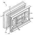
- FIG. 1 is an exploded perspective view showing a plasma display apparatus according to an exemplary embodiment of the present invention.
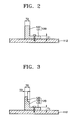
- FIG. 2 is a cross-sectional view of a reinforcement member taken along line 11 - 11 of FIG. 1 .
- FIG. 3 is a cross-sectional view of another exemplary embodiment of the reinforcement member of FIG. 2 .
- FIG. 4 is a cross-sectional view of a reinforcement member taken along line IV-IV of FIG. 1 .
- FIG. 5 is a cross-sectional view of another exemplary embodiment of the reinforcement member of FIG. 4 .
- FIG. 1 is an exploded perspective view showing a plasma display apparatus according to an exemplary embodiment of the present invention.
- a plasma display apparatus 100 may include a panel 111 , a chassis base 112 coupled to the panel 111 , and a circuit board 113 installed on a rear side of the chassis base 112 .
- the panel 111 comprises a front panel and a rear panel.
- the front panel may include a plurality of stripe-shaped sustain electrodes, bus electrodes connected to each sustain electrode, a front dielectric layer covering the sustain electrodes and the bus electrodes, and a protective layer covering the front dielectric layer.
- the rear panel faces the front panel, and it may include a plurality of address electrodes arranged perpendicularly to the sustain electrodes, a rear dielectric layer covering the address electrodes, barrier ribs formed on the rear dielectric layer to define a discharge space and prevent cross-talk, and red, green, and blue phosphor layers coated on the rear dielectric layer and sides of the barrier ribs.
- An electromagnetic interference filter may be installed on the entire surface of the panel 111 to prevent electromagnetic waves from harming viewers.
- the chassis base 112 may be disposed at the rear of the panel 111 to support the panel and emit heat transferred from it.
- An adhesive member 115 may couple the panel 111 to the chassis base 112 .
- a panel heat-dissipation member 114 i.e. a thermal conductive medium
- It dissipates heat generated in the panel 111 via the chassis base 112 .
- the circuit board 113 may be mounted on the rear of the chassis base 112 , and it may accommodate electronic components for driving the panel 111 .
- the electronic components may include a variety of components, such as components for supplying power to the panel and components for applying image-forming signals to the panel.
- the panel 111 , the chassis base 112 , and the circuit board 113 may be housed in a case (not shown).
- Reinforcement members 120 and 130 may be installed on the rear side of the chassis base 112 to prevent the chassis base 112 from twisting or bending.
- the reinforcement members 120 and 130 may include center reinforcement members 120 installed in the center of the chassis base and side reinforcement members 130 installed at edges of the chassis base.
- the center reinforcement members 120 may include a widthwise reinforcement member installed along a width of the chassis base 112 and a lengthwise reinforcement member installed along a length direction of the chassis base 112 .
- the side reinforcement members 130 may include a widthwise reinforcement member and a lengthwise reinforcement member.
- the circuit board 113 may be disposed on the rear side of the chassis base 112 and in a space between the reinforcement members 120 and 130 .
- the reinforcement members 120 and 130 may be disposed symmetrically with the rear side of the chassis base 112 to more uniformly distribute stress occurring in the reinforcement members 120 and 130 due to an external force or thermal expansion.
- the reinforcement members 120 and 130 may be formed of a stiff material in order to stably support the chassis base 112 .
- Aluminum, steel, or other stiff and workable materials may be used.
- the reinforcement members 120 and 130 may have various cross-sectional structures.
- FIG. 2 shows a cross-sectional structure of the reinforcement members 120 taken along line 11 - 11 of FIG. 1 .
- the reinforcement members 120 may include a base portion 121 , which may be coupled to the chassis base 112 , and and an extended portion 122 that bends from the base portion 121 .
- T 1 is a cross-sectional thickness of the base portion 121
- T 2 is a cross-sectional thickness of the extended portion 122
- T 1 is not equal to T 2 .
- the base portion 121 may be set to be about 0.75 to about 1.5 times the thickness of the chassis base 112 .
- the cross-sectional thickness T 2 of the extended portion 122 may be greater than the cross-sectional thickness T 1 of the base portion 121 .
- the weight of the reinforcement members 120 increases.
- the ratio of the cross-sectional thickness T 2 to the cross-sectional thickness T 1 may be in a range of about 1.2 to about 3.
- the reinforcement members 120 may be extrusion molded to form the above-described cross-sectional structure.
- Table 1 shows measured values of chassis base is stiffness according to a cross-sectional thickness T 2 of an extended portion 122 .
- T1 (mm) T2 (mm) Stiffness (%) 1.6 1.6 100 1.6 2.0 110 1.6 2.5 119 1.6 3.0 126 1.6 3.2 129 1.6 3.5 131
- FIG. 3 shows an alternative cross-sectional structure of the reinforcement members 120 .
- a stepped portion 123 may be formed in the extended portion 122 of the reinforcement members 120 .
- FIG. 3 shows a cross-sectional thickness T 3 of the stepped portion 123 as less than the cross-sectional thickness T 2 of the extended portion 122 .
- T 3 may be greater than T 2 .
- the stepped portion 123 may be formed in a portion of the extended portion 122 , and the ratio of the cross-sectional thickness T 2 to the cross-sectional thickness T 3 may be in a range of about 0.8 to about 2.
- FIG. 4 is a cross-sectional view of the reinforcement member 130 taken along line IV-IV of FIG. 1 .
- a reinforcement member 130 may include a base portion 131 , an extended portion 132 , and a connection portion 133 .
- the base portion 131 may include first and second base portions 131 a and 131 b , separated from each other by a gap, and coupled to the chassis base 112 .
- the extended portion 132 may include first and second extended portions 132 a and 132 b , which may be bent from the first and second base portions 131 a and 131 b , respectively, and the connection portion 133 connects the first and second extended portions 132 a and 132 b.
- T 4 is a cross-sectional thickness of the first and second base portions 131 a and 131 b
- T 5 is a cross-sectional thickness of the first and second extended portions 132 a and 132 b
- T 4 is not equal to T 5 .
- the cross-sectional thickness T 4 of the first and second base portions 131 a and 131 b may be in a range of about 0.75 to about 1.5 times the thickness of the chassis base 112 .
- the cross-sectional thickness T 5 may be greater than the cross-sectional thickness T 4 . Additionally, a cross-sectional thickness T 7 of the connection portion 133 may be equal to or approximately equal to the cross-sectional thickness T 4 of the first and second base portions 131 a and 131 b.
- the weight of the reinforcement member 130 increases.
- the ratio of the cross-sectional thickness T 5 to the cross-sectional thickness T 4 i.e. T 5 /T 4
- the reinforcement members 130 may be extrusion molded to form the above-described cross-sectional structure.
- FIG. 5 shows an alternative cross-sectional structure of the reinforcement member 130 .
- a stepped portion 134 may be formed in the extended portion 132 of the reinforcement members 130 .
- first and second stepped portions 134 a and 134 b may be formed in the first and second extended portions 132 a and 132 b .
- FIG. 5 shows the cross-sectional thickness T 5 of the first and second extended portions 132 a and 132 b as greater than the cross-sectional thickness T 6 of the first and second stepped portions 134 a and 134 b .
- the thickness T 6 of the first and second stepped portions 134 a and 134 b may be greater than the thickness T 5 of each of the first and second extended portions 132 a and 132 b.
- the first and second stepped portions 134 a and 134 b may be formed in portions of the first and second extended portions 132 a and 132 b , and the ratio of the cross-sectional thickness T 5 of the first and second extended portions 132 a and 132 b to the cross-sectional thickness T 6 of the first and second stepped portions 134 a and 134 b may be in a range of about 0.8 to about 2.
- a reinforcement member may have a cross-sectional structure with an increased area moment of inertia, thereby stiffening a chassis base and minimizing twisting and deflection of the chassis base.
- a proper number of reinforcement members may be installed to maximize the reinforcement of the chassis base.
- the reinforcement members may be installed in an appropriate place on the chassis base, thereby is increasing utility of the space on the rear side of the chassis base. Additionally, manufacturing costs of the chassis base may be reduced.
Landscapes
- Engineering & Computer Science (AREA)
- General Engineering & Computer Science (AREA)
- Theoretical Computer Science (AREA)
- Computer Hardware Design (AREA)
- Human Computer Interaction (AREA)
- Physics & Mathematics (AREA)
- General Physics & Mathematics (AREA)
- Multimedia (AREA)
- Devices For Indicating Variable Information By Combining Individual Elements (AREA)
Abstract
Description
- This application claims priority to and the benefit of Korean Patent Application No. 10-2004-0010667, filed on Feb. 18, 2004, which is hereby incorporated by reference for all purposes as if fully set forth herein.
- 1. Field of the Invention
- The present invention relates to a plasma display apparatus, and more particularly, to a plasma display apparatus having a reinforcement member installed on a chassis base.
- 2. Description of the Background
- Generally, a plasma display apparatus is a flat panel display apparatus. Its is display panel forms an image using light emitted by ultraviolet rays generated by a gas discharge in a discharge space. The plasma display apparatus may be a few centimeters thick, and it may have a large screen and a wide view-angle of about 150° or more.
- To manufacture a plasma display apparatus, a front panel and a rear panel may be joined together, a chassis base may be coupled to the rear of the combined panel, and a circuit board may be mounted on the chassis base.
- Since the chassis base emits heat generated in the panel and supports the panel, it is typically made of a metal, such as aluminum, having high thermal conductivity.
- The chassis base should be thin in order to obtain a thinner plasma display apparatus. However, if thinly made, it may not properly support the panel. Thus, reinforcement members may be installed on a rear side of the chassis base to prevent it from twisting or bending.
- Multiple reinforcement members may be installed on the rear side of the chassis base. However, the reinforcement members share limited space on the rear of the chassis with other components, such as circuit boards. Therefore, having too many reinforcement members may add difficulties to the design and manufacturing processes, as well as increase costs.
- Accordingly, reinforcement members should be optimally designed so that they may be appropriately installed in the limited space available on the chassis base.
- The present invention provides reinforcement members of a plasma display apparatus that may provide stronger reinforcement with fewer members, thereby reducing the apparatus' manufacturing costs.
- Additional features of the invention will be set forth in the description which follows, and in part will be apparent from the description, or may be learned by practice of the invention.
- The present invention discloses a plasma display apparatus comprising a display panel, a chassis base coupled to a rear of the display panel, and a reinforcement member. The reinforcement member includes a base portion coupled to the chassis base and and an extended portion bent from the base portion. A cross-sectional thickness of the extended portion is different from a cross-sectional thickness of the base portion.
- It is to be understood that both the foregoing general description and the following detailed description are exemplary and explanatory and are intended to provide further explanation of the invention as claimed.
- The accompanying drawings, which are included to provide a further understanding of the invention and are incorporated in and constitute a part of this specification, illustrate embodiments of the invention and together with the description serve to explain the principles of the invention.
-
FIG. 1 is an exploded perspective view showing a plasma display apparatus according to an exemplary embodiment of the present invention. -
FIG. 2 is a cross-sectional view of a reinforcement member taken along line 11-11 ofFIG. 1 . -
FIG. 3 is a cross-sectional view of another exemplary embodiment of the reinforcement member ofFIG. 2 . -
FIG. 4 is a cross-sectional view of a reinforcement member taken along line IV-IV ofFIG. 1 . -
FIG. 5 is a cross-sectional view of another exemplary embodiment of the reinforcement member ofFIG. 4 . -
FIG. 1 is an exploded perspective view showing a plasma display apparatus according to an exemplary embodiment of the present invention. Referring toFIG. 1 , aplasma display apparatus 100 may include apanel 111, achassis base 112 coupled to thepanel 111, and acircuit board 113 installed on a rear side of thechassis base 112. - The
panel 111 comprises a front panel and a rear panel. The front panel may include a plurality of stripe-shaped sustain electrodes, bus electrodes connected to each sustain electrode, a front dielectric layer covering the sustain electrodes and the bus electrodes, and a protective layer covering the front dielectric layer. - The rear panel faces the front panel, and it may include a plurality of address electrodes arranged perpendicularly to the sustain electrodes, a rear dielectric layer covering the address electrodes, barrier ribs formed on the rear dielectric layer to define a discharge space and prevent cross-talk, and red, green, and blue phosphor layers coated on the rear dielectric layer and sides of the barrier ribs. An electromagnetic interference filter may be installed on the entire surface of the
panel 111 to prevent electromagnetic waves from harming viewers. - The
chassis base 112 may be disposed at the rear of thepanel 111 to support the panel and emit heat transferred from it. - An
adhesive member 115, such as double sided tape, may couple thepanel 111 to thechassis base 112. A panel heat-dissipation member 114 (i.e. a thermal conductive medium) may be disposed between thepanel 111 and thechassis base 112. It dissipates heat generated in thepanel 111 via thechassis base 112. - The
circuit board 113 may be mounted on the rear of thechassis base 112, and it may accommodate electronic components for driving thepanel 111. The electronic components may include a variety of components, such as components for supplying power to the panel and components for applying image-forming signals to the panel. Thepanel 111, thechassis base 112, and thecircuit board 113 may be housed in a case (not shown). -
Reinforcement members chassis base 112 to prevent thechassis base 112 from twisting or bending. - In order to increase reinforcement of the
chassis base 112, thereinforcement members center reinforcement members 120 installed in the center of the chassis base andside reinforcement members 130 installed at edges of the chassis base. - The
center reinforcement members 120 may include a widthwise reinforcement member installed along a width of thechassis base 112 and a lengthwise reinforcement member installed along a length direction of thechassis base 112. Similarly, theside reinforcement members 130 may include a widthwise reinforcement member and a lengthwise reinforcement member. As described above, thecircuit board 113 may be disposed on the rear side of thechassis base 112 and in a space between thereinforcement members - The
reinforcement members chassis base 112 to more uniformly distribute stress occurring in thereinforcement members - The
reinforcement members chassis base 112. Aluminum, steel, or other stiff and workable materials may be used. - The
reinforcement members FIG. 2 shows a cross-sectional structure of thereinforcement members 120 taken along line 11-11 ofFIG. 1 . - Referring to
FIG. 2 , thereinforcement members 120 may include abase portion 121, which may be coupled to thechassis base 112, and and an extendedportion 122 that bends from thebase portion 121. T1 is a cross-sectional thickness of thebase portion 121, T2 is a cross-sectional thickness of the extendedportion 122, and T1 is not equal to T2. - Since the cross-sectional thickness T1 of the
base portion 121 does not significantly affect chassis base stiffness, unlike the cross-sectional thickness T2 of theextended portion 122, thebase portion 121 may be set to be about 0.75 to about 1.5 times the thickness of thechassis base 112. - The cross-sectional thickness T2 of the extended
portion 122 may be greater than the cross-sectional thickness T1 of thebase portion 121. - As the cross-sectional thickness T2 increases, the weight of the
reinforcement members 120 increases. Thus, the ratio of the cross-sectional thickness T2 to the cross-sectional thickness T1 may be in a range of about 1.2 to about 3. Additionally, thereinforcement members 120 may be extrusion molded to form the above-described cross-sectional structure. - As the cross-sectional thickness T2 increases, an area moment of inertia and reinforcement of the chassis base increase, thereby providing a
stiffer chassis base 112 and minimizing its twisting and bending. - This effect is shown in Table 1, which shows measured values of chassis base is stiffness according to a cross-sectional thickness T2 of an
extended portion 122.TABLE 1 T1 (mm) T2 (mm) Stiffness (%) 1.6 1.6 100 1.6 2.0 110 1.6 2.5 119 1.6 3.0 126 1.6 3.2 129 1.6 3.5 131 - The stiffness of the
chassis base 112 is defined by dividing deflection of the chassis base by the weight applied to it. Assuming that the stiffness is 100% when T2=T1, Table 1 shows that as T2 increases, the chassis base stiffens. -
FIG. 3 shows an alternative cross-sectional structure of thereinforcement members 120. - Referring to
FIG. 3 , a steppedportion 123 may be formed in theextended portion 122 of thereinforcement members 120.FIG. 3 shows a cross-sectional thickness T3 of the steppedportion 123 as less than the cross-sectional thickness T2 of theextended portion 122. However, T3 may be greater than T2. - The stepped
portion 123 may be formed in a portion of theextended portion 122, and the ratio of the cross-sectional thickness T2 to the cross-sectional thickness T3 may be in a range of about 0.8 to about 2. -
FIG. 4 is a cross-sectional view of thereinforcement member 130 taken along line IV-IV ofFIG. 1 . - Referring to
FIG. 4 , areinforcement member 130 may include abase portion 131, anextended portion 132, and aconnection portion 133. Thebase portion 131 may include first andsecond base portions chassis base 112. Theextended portion 132 may include first and secondextended portions second base portions connection portion 133 connects the first and secondextended portions - T4 is a cross-sectional thickness of the first and
second base portions extended portions - Similar to the previous exemplary embodiment, the cross-sectional thickness T4 of the first and
second base portions chassis base 112. - The cross-sectional thickness T5 may be greater than the cross-sectional thickness T4. Additionally, a cross-sectional thickness T7 of the
connection portion 133 may be equal to or approximately equal to the cross-sectional thickness T4 of the first andsecond base portions - As the cross-sectional thickness T5 increases, the weight of the
reinforcement member 130 increases. Hence, the ratio of the cross-sectional thickness T5 to the cross-sectional thickness T4 (i.e. T5/T4) may be in a range of about 1.2 to about 3. Additionally, thereinforcement members 130 may be extrusion molded to form the above-described cross-sectional structure. - As the cross-sectional thickness T5 increases, an area moment of inertia and reinforcement of the chassis base increase, thereby stiffening the panel and minimizing its twisting and bending.
-
FIG. 5 shows an alternative cross-sectional structure of thereinforcement member 130. - Referring to
FIG. 5 , a steppedportion 134 may be formed in theextended portion 132 of thereinforcement members 130. In other words, first and second steppedportions extended portions FIG. 5 shows the cross-sectional thickness T5 of the first and secondextended portions portions portions extended portions - The first and second stepped
portions extended portions extended portions portions - As described above, in the plasma display apparatus according to exemplary embodiments of the present invention, a reinforcement member may have a cross-sectional structure with an increased area moment of inertia, thereby stiffening a chassis base and minimizing twisting and deflection of the chassis base. A proper number of reinforcement members may be installed to maximize the reinforcement of the chassis base. Further, the reinforcement members may be installed in an appropriate place on the chassis base, thereby is increasing utility of the space on the rear side of the chassis base. Additionally, manufacturing costs of the chassis base may be reduced.
- It will be apparent to those skilled in the art that various modifications and variation can be made in the present invention without departing from the spirit or scope of the invention. Thus, it is intended that the present invention cover the modifications and variations of this invention provided they come within the scope of the appended claims and their equivalents.
Claims (14)
Applications Claiming Priority (2)
| Application Number | Priority Date | Filing Date | Title |
|---|---|---|---|
| KR1020040010667A KR100603331B1 (en) | 2004-02-18 | 2004-02-18 | Plasma display apparatus |
| KR04-10667 | 2004-02-18 |
Publications (2)
| Publication Number | Publication Date |
|---|---|
| US20050180098A1 true US20050180098A1 (en) | 2005-08-18 |
| US7321487B2 US7321487B2 (en) | 2008-01-22 |
Family
ID=34836806
Family Applications (1)
| Application Number | Title | Priority Date | Filing Date |
|---|---|---|---|
| US11/054,941 Expired - Fee Related US7321487B2 (en) | 2004-02-18 | 2005-02-11 | Plasma display apparatus |
Country Status (4)
| Country | Link |
|---|---|
| US (1) | US7321487B2 (en) |
| JP (1) | JP2005234577A (en) |
| KR (1) | KR100603331B1 (en) |
| CN (1) | CN100504970C (en) |
Cited By (8)
| Publication number | Priority date | Publication date | Assignee | Title |
|---|---|---|---|---|
| US20050264982A1 (en) * | 2004-05-18 | 2005-12-01 | Guy-Seong Kim | Plasma display apparatus |
| US20060098415A1 (en) * | 2004-11-10 | 2006-05-11 | Ki-Jung Kim | Plasma display panel (PDP) supporting member and PDP including the supporting member |
| US20060274486A1 (en) * | 2005-06-04 | 2006-12-07 | Kim Yeung-Ki | Plasma display panel |
| US20070086149A1 (en) * | 2005-10-18 | 2007-04-19 | Young-Oh Choi | Plasma display device |
| US20070091223A1 (en) * | 2005-10-21 | 2007-04-26 | Funai Electric Co.,Ltd. | Panel type television and LCD television |
| US20090161306A1 (en) * | 2006-05-16 | 2009-06-25 | Start Design By Javi Crespo, S.L. | Computer monitor protector |
| US7872703B2 (en) | 2007-08-20 | 2011-01-18 | Funai Electric Co., Ltd. | Display module supporting structure |
| US20130155655A1 (en) * | 2011-12-19 | 2013-06-20 | Moungyoub Lee | Display apparatus |
Families Citing this family (8)
| Publication number | Priority date | Publication date | Assignee | Title |
|---|---|---|---|---|
| KR100683720B1 (en) * | 2004-12-02 | 2007-02-15 | 삼성에스디아이 주식회사 | Chassis reinforcement structure and plasma display device having same |
| JP2007206646A (en) * | 2006-02-06 | 2007-08-16 | Sharp Corp | Display device |
| JP4786366B2 (en) * | 2006-02-20 | 2011-10-05 | 日立プラズマディスプレイ株式会社 | Plasma display device |
| JP4967491B2 (en) * | 2006-07-14 | 2012-07-04 | パナソニック株式会社 | Plasma display device |
| KR100807027B1 (en) * | 2006-10-13 | 2008-02-25 | 삼성에스디아이 주식회사 | Plasma display device |
| TWM314868U (en) * | 2006-11-27 | 2007-07-01 | Innolux Display Corp | Backlight module and liquid crystal display using same |
| USD702670S1 (en) * | 2009-03-26 | 2014-04-15 | Tait Towers Manufacturing, LLC | Video screen frame |
| USD676029S1 (en) * | 2012-06-15 | 2013-02-12 | Peerless Industries, Inc. | System for mounting audio/visual devices or the like from an overhead structure |
Citations (5)
| Publication number | Priority date | Publication date | Assignee | Title |
|---|---|---|---|---|
| US6411501B1 (en) * | 1998-11-11 | 2002-06-25 | Lg Philips Lcd Co., Ltd. | Portable computer and method for mounting a flat display device module |
| US6545733B2 (en) * | 1995-04-18 | 2003-04-08 | Canon Kabushiki Kaisha | Display apparatus |
| US20030122992A1 (en) * | 2001-12-27 | 2003-07-03 | Fujitsu Limited | Liquid crystal display device with hooks |
| US6688576B2 (en) * | 2001-04-23 | 2004-02-10 | Pioneer Corporation | Display apparatus |
| US7006167B2 (en) * | 2000-05-26 | 2006-02-28 | Nec Corporation | Fixing structure for an LCD panel |
Family Cites Families (6)
| Publication number | Priority date | Publication date | Assignee | Title |
|---|---|---|---|---|
| JP2001337611A (en) | 2000-03-22 | 2001-12-07 | Furukawa Electric Co Ltd:The | Display frame |
| JP2002099218A (en) | 2000-09-22 | 2002-04-05 | Nec Corp | Plasma display panel device having reinforcing plate |
| JP2003029643A (en) | 2001-07-18 | 2003-01-31 | Mitsubishi Electric Corp | Display device |
| KR100420026B1 (en) * | 2001-10-27 | 2004-02-25 | 삼성에스디아이 주식회사 | Plasma Display Device |
| JP2003216057A (en) | 2001-11-14 | 2003-07-30 | Canon Inc | Image display unit |
| KR100450195B1 (en) * | 2002-04-22 | 2004-09-24 | 삼성에스디아이 주식회사 | Plasma display device |
-
2004
- 2004-02-18 KR KR1020040010667A patent/KR100603331B1/en not_active Expired - Fee Related
-
2005
- 2005-02-11 US US11/054,941 patent/US7321487B2/en not_active Expired - Fee Related
- 2005-02-17 JP JP2005040929A patent/JP2005234577A/en active Pending
- 2005-02-18 CN CNB2005100565741A patent/CN100504970C/en not_active Expired - Fee Related
Patent Citations (5)
| Publication number | Priority date | Publication date | Assignee | Title |
|---|---|---|---|---|
| US6545733B2 (en) * | 1995-04-18 | 2003-04-08 | Canon Kabushiki Kaisha | Display apparatus |
| US6411501B1 (en) * | 1998-11-11 | 2002-06-25 | Lg Philips Lcd Co., Ltd. | Portable computer and method for mounting a flat display device module |
| US7006167B2 (en) * | 2000-05-26 | 2006-02-28 | Nec Corporation | Fixing structure for an LCD panel |
| US6688576B2 (en) * | 2001-04-23 | 2004-02-10 | Pioneer Corporation | Display apparatus |
| US20030122992A1 (en) * | 2001-12-27 | 2003-07-03 | Fujitsu Limited | Liquid crystal display device with hooks |
Cited By (16)
| Publication number | Priority date | Publication date | Assignee | Title |
|---|---|---|---|---|
| US20050264982A1 (en) * | 2004-05-18 | 2005-12-01 | Guy-Seong Kim | Plasma display apparatus |
| US7453528B2 (en) * | 2004-05-18 | 2008-11-18 | Samsung Co., Ltd. | Plasma display apparatus |
| US20060098415A1 (en) * | 2004-11-10 | 2006-05-11 | Ki-Jung Kim | Plasma display panel (PDP) supporting member and PDP including the supporting member |
| US7492578B2 (en) * | 2005-06-04 | 2009-02-17 | Samsung Sdi Co., Ltd. | Plasma display panel |
| US20060274486A1 (en) * | 2005-06-04 | 2006-12-07 | Kim Yeung-Ki | Plasma display panel |
| US20070086149A1 (en) * | 2005-10-18 | 2007-04-19 | Young-Oh Choi | Plasma display device |
| EP1777955A3 (en) * | 2005-10-21 | 2009-08-12 | Funai Electric Co., Ltd. | Panel type television and LCD television |
| US20070091223A1 (en) * | 2005-10-21 | 2007-04-26 | Funai Electric Co.,Ltd. | Panel type television and LCD television |
| US7868951B2 (en) | 2005-10-21 | 2011-01-11 | Funai Electric Co., Ltd. | Panel type television and LCD television |
| US20090161306A1 (en) * | 2006-05-16 | 2009-06-25 | Start Design By Javi Crespo, S.L. | Computer monitor protector |
| US7872703B2 (en) | 2007-08-20 | 2011-01-18 | Funai Electric Co., Ltd. | Display module supporting structure |
| US20130155655A1 (en) * | 2011-12-19 | 2013-06-20 | Moungyoub Lee | Display apparatus |
| US9320138B2 (en) | 2011-12-19 | 2016-04-19 | Lg Electronics Inc. | Display apparatus |
| US9608231B2 (en) | 2011-12-19 | 2017-03-28 | Lg Electronics Inc. | Display apparatus |
| US9711752B2 (en) * | 2011-12-19 | 2017-07-18 | Lg Electronics Inc. | Display apparatus |
| US10181575B2 (en) | 2011-12-19 | 2019-01-15 | Lg Electronics Inc. | Display apparatus |
Also Published As
| Publication number | Publication date |
|---|---|
| KR100603331B1 (en) | 2006-07-20 |
| US7321487B2 (en) | 2008-01-22 |
| CN1658256A (en) | 2005-08-24 |
| JP2005234577A (en) | 2005-09-02 |
| KR20050082257A (en) | 2005-08-23 |
| CN100504970C (en) | 2009-06-24 |
Similar Documents
| Publication | Publication Date | Title |
|---|---|---|
| US7321487B2 (en) | Plasma display apparatus | |
| US7394186B2 (en) | Display apparatus | |
| US5587624A (en) | Plasma display panel | |
| US7133281B2 (en) | Display device and heat dissipating chassis therefor | |
| US6847156B2 (en) | Plasma display device with heat radiating plate | |
| US7619891B2 (en) | Plasma display apparatus | |
| US20090316371A1 (en) | Plasma display module, display device including the same, and associated methods | |
| KR102492586B1 (en) | Display device | |
| US7864545B2 (en) | Chassis base assembly and plasma display panel (PDP) assembly including the chassis base assembly | |
| US20050099126A1 (en) | Plasma display panel with discharge cells having curved concave-shaped walls | |
| US7492099B2 (en) | Plasma display device | |
| US7629748B2 (en) | Plasma display apparatus | |
| US20060083901A1 (en) | Double sided tape for attaching plasma display panel and plasma display apparatus having the same | |
| US8143785B2 (en) | Plasma display device having an anisotropic conductive film | |
| US20060091773A1 (en) | Plasma display device | |
| US20090315879A1 (en) | Plasma display device | |
| KR100749471B1 (en) | Plasma display device | |
| US20100141561A1 (en) | Plasma display device | |
| KR100612348B1 (en) | Plasma display device | |
| JP2002116710A (en) | Plasma display device and its manufacturing method | |
| KR100669798B1 (en) | Reinforcement structure of chassis base of plasma display device | |
| KR100637143B1 (en) | Plasma display | |
| KR100603385B1 (en) | Plasma display module | |
| KR100433214B1 (en) | Plasma display panel | |
| KR100502918B1 (en) | Plasma display device |
Legal Events
| Date | Code | Title | Description |
|---|---|---|---|
| AS | Assignment |
Owner name: SAMSUNG SDI CO., LTD., KOREA, REPUBLIC OF Free format text: ASSIGNMENT OF ASSIGNORS INTEREST;ASSIGNOR:KIM, SOK-SAN;REEL/FRAME:016271/0443 Effective date: 20050128 |
|
| FEPP | Fee payment procedure |
Free format text: PAYOR NUMBER ASSIGNED (ORIGINAL EVENT CODE: ASPN); ENTITY STATUS OF PATENT OWNER: LARGE ENTITY |
|
| FEPP | Fee payment procedure |
Free format text: PAYOR NUMBER ASSIGNED (ORIGINAL EVENT CODE: ASPN); ENTITY STATUS OF PATENT OWNER: LARGE ENTITY Free format text: PAYER NUMBER DE-ASSIGNED (ORIGINAL EVENT CODE: RMPN); ENTITY STATUS OF PATENT OWNER: LARGE ENTITY |
|
| FPAY | Fee payment |
Year of fee payment: 4 |
|
| REMI | Maintenance fee reminder mailed | ||
| LAPS | Lapse for failure to pay maintenance fees | ||
| STCH | Information on status: patent discontinuation |
Free format text: PATENT EXPIRED DUE TO NONPAYMENT OF MAINTENANCE FEES UNDER 37 CFR 1.362 |
|
| STCH | Information on status: patent discontinuation |
Free format text: PATENT EXPIRED DUE TO NONPAYMENT OF MAINTENANCE FEES UNDER 37 CFR 1.362 |
|
| FP | Lapsed due to failure to pay maintenance fee |
Effective date: 20160122 |