US20030198067A1 - Core structure and interleaved DC-DC converter topology - Google Patents
Core structure and interleaved DC-DC converter topology Download PDFInfo
- Publication number
- US20030198067A1 US20030198067A1 US10/302,095 US30209502A US2003198067A1 US 20030198067 A1 US20030198067 A1 US 20030198067A1 US 30209502 A US30209502 A US 30209502A US 2003198067 A1 US2003198067 A1 US 2003198067A1
- Authority
- US
- United States
- Prior art keywords
- post
- converter
- wound
- base
- core
- Prior art date
- Legal status (The legal status is an assumption and is not a legal conclusion. Google has not performed a legal analysis and makes no representation as to the accuracy of the status listed.)
- Granted
Links
- 238000004804 winding Methods 0.000 claims description 166
- 239000003990 capacitor Substances 0.000 claims description 13
- 230000005669 field effect Effects 0.000 claims 2
- 230000004907 flux Effects 0.000 abstract description 22
- 238000013461 design Methods 0.000 abstract description 16
- 239000000463 material Substances 0.000 abstract description 6
- 230000001413 cellular effect Effects 0.000 abstract description 2
- 229910000859 α-Fe Inorganic materials 0.000 abstract description 2
- 210000004027 cell Anatomy 0.000 description 27
- 238000010586 diagram Methods 0.000 description 18
- 230000005291 magnetic effect Effects 0.000 description 14
- 238000012546 transfer Methods 0.000 description 9
- 230000001965 increasing effect Effects 0.000 description 8
- 230000008901 benefit Effects 0.000 description 4
- 210000003850 cellular structure Anatomy 0.000 description 3
- 238000001816 cooling Methods 0.000 description 3
- 230000010354 integration Effects 0.000 description 3
- 230000008878 coupling Effects 0.000 description 2
- 238000010168 coupling process Methods 0.000 description 2
- 238000005859 coupling reaction Methods 0.000 description 2
- 230000003071 parasitic effect Effects 0.000 description 2
- 230000003362 replicative effect Effects 0.000 description 2
- 239000007787 solid Substances 0.000 description 2
- RYGMFSIKBFXOCR-UHFFFAOYSA-N Copper Chemical compound [Cu] RYGMFSIKBFXOCR-UHFFFAOYSA-N 0.000 description 1
- 229910000640 Fe alloy Inorganic materials 0.000 description 1
- BQCADISMDOOEFD-UHFFFAOYSA-N Silver Chemical compound [Ag] BQCADISMDOOEFD-UHFFFAOYSA-N 0.000 description 1
- 239000000654 additive Substances 0.000 description 1
- 230000000996 additive effect Effects 0.000 description 1
- 229910045601 alloy Inorganic materials 0.000 description 1
- 239000000956 alloy Substances 0.000 description 1
- 229910052782 aluminium Inorganic materials 0.000 description 1
- XAGFODPZIPBFFR-UHFFFAOYSA-N aluminium Chemical compound [Al] XAGFODPZIPBFFR-UHFFFAOYSA-N 0.000 description 1
- 239000000919 ceramic Substances 0.000 description 1
- 239000002131 composite material Substances 0.000 description 1
- 239000004020 conductor Substances 0.000 description 1
- 229910052802 copper Inorganic materials 0.000 description 1
- 239000010949 copper Substances 0.000 description 1
- 230000003247 decreasing effect Effects 0.000 description 1
- 230000007123 defense Effects 0.000 description 1
- 238000003870 depth resolved spectroscopy Methods 0.000 description 1
- 238000011161 development Methods 0.000 description 1
- 208000009743 drug hypersensitivity syndrome Diseases 0.000 description 1
- 230000009977 dual effect Effects 0.000 description 1
- 238000004146 energy storage Methods 0.000 description 1
- PCHJSUWPFVWCPO-UHFFFAOYSA-N gold Chemical compound [Au] PCHJSUWPFVWCPO-UHFFFAOYSA-N 0.000 description 1
- 229910052737 gold Inorganic materials 0.000 description 1
- 239000010931 gold Substances 0.000 description 1
- 230000001939 inductive effect Effects 0.000 description 1
- UGKDIUIOSMUOAW-UHFFFAOYSA-N iron nickel Chemical compound [Fe].[Ni] UGKDIUIOSMUOAW-UHFFFAOYSA-N 0.000 description 1
- 230000001788 irregular Effects 0.000 description 1
- 238000004519 manufacturing process Methods 0.000 description 1
- 239000011159 matrix material Substances 0.000 description 1
- 238000000034 method Methods 0.000 description 1
- 239000012256 powdered iron Substances 0.000 description 1
- 238000011160 research Methods 0.000 description 1
- 238000000926 separation method Methods 0.000 description 1
Images


Classifications
-
- H—ELECTRICITY
- H02—GENERATION; CONVERSION OR DISTRIBUTION OF ELECTRIC POWER
- H02M—APPARATUS FOR CONVERSION BETWEEN AC AND AC, BETWEEN AC AND DC, OR BETWEEN DC AND DC, AND FOR USE WITH MAINS OR SIMILAR POWER SUPPLY SYSTEMS; CONVERSION OF DC OR AC INPUT POWER INTO SURGE OUTPUT POWER; CONTROL OR REGULATION THEREOF
- H02M7/00—Conversion of AC power input into DC power output; Conversion of DC power input into AC power output
- H02M7/02—Conversion of AC power input into DC power output without possibility of reversal
- H02M7/04—Conversion of AC power input into DC power output without possibility of reversal by static converters
- H02M7/043—Conversion of AC power input into DC power output without possibility of reversal by static converters using transformers or inductors only
-
- H—ELECTRICITY
- H01—ELECTRIC ELEMENTS
- H01F—MAGNETS; INDUCTANCES; TRANSFORMERS; SELECTION OF MATERIALS FOR THEIR MAGNETIC PROPERTIES
- H01F3/00—Cores, Yokes, or armatures
- H01F3/08—Cores, Yokes, or armatures made from powder
-
- H—ELECTRICITY
- H01—ELECTRIC ELEMENTS
- H01F—MAGNETS; INDUCTANCES; TRANSFORMERS; SELECTION OF MATERIALS FOR THEIR MAGNETIC PROPERTIES
- H01F30/00—Fixed transformers not covered by group H01F19/00
- H01F30/06—Fixed transformers not covered by group H01F19/00 characterised by the structure
-
- H—ELECTRICITY
- H01—ELECTRIC ELEMENTS
- H01F—MAGNETS; INDUCTANCES; TRANSFORMERS; SELECTION OF MATERIALS FOR THEIR MAGNETIC PROPERTIES
- H01F17/00—Fixed inductances of the signal type
- H01F17/04—Fixed inductances of the signal type with magnetic core
Definitions
- This invention relates to the field of DC-DC converters, and particularly to core structures and converter topologies which achieve small output voltage ripple.
- Power converters are key components in many military and commercial systems and they often govern size and performance. Power density, efficiency and reliability are key characteristics used to evaluate the characteristics of power converters. Transformers and inductors used within these power converters may be large and bulky and often limit their efficiency, power density and reliability.
- E-core has a cross-section that looks like the capital letter “E.”
- E-core is typically disposed on its side, with the long part of the E at the bottom, forming a base. E-cores are commonly used in current doubler circuits.
- E-cores typically have one of two configurations—the EI-core or the EE-core.
- the EI-core a flat plate, the “I,” is disposed on top of the basic E-core.
- the EE-core two Es are put together, with the legs of the Es facing each other.
- the EI-core, the EE-core and other cores incorporating the E core structure are referred to generically as E-cores.
- E-cores are typically used for transformers and inductors, and a single E-core may be adapted for use as both a transformer and an inductor.
- both of the outer legs have a primary and a secondary winding. Voltage to the windings is typically switched so that only one outer leg at any given time is acting as a transformer.
- the device is said to have one or two switching periods during which the inductors charge, and a freewheeling period during which the inductors discharge.
- the circuitry provides for one outer leg to act as an inductor while the other outer leg is acting as a transformer. Because of their dual but time-separated nature, the outer legs are said to have a transformer phase and an inductor phase.
- E-cores can be isolated (without transformers) or non-isolated (with transformers). E-cores may also be used only as transformers.
- an outer leg of an E-core When an outer leg of an E-core is acting as an inductor, magnetic flux is stored in the core. Magnetic flux flows through the outer leg which is acting as an inductor, through the top, the base, and through the center leg of the E. To provide increased energy storage, there is typically an air gap between the center leg and the top. Because of the air gap, the center leg is therefore typically shorter than the outer legs. Inductance in an E-core is primarily determined by the area of the center leg. To obtain higher inductance, the area of the center leg is increased.
- fringing flux Like bright light from one room leaking under a door into a dark second room, flux from the air gap can spill onto the outer legs. Fringing flux causes current losses in the transformer of the other outer leg.
- One way to accommodate fringing flux is to place the windings on the outer legs a safe distance from the air gap. To do this, the outer legs may be far from the center leg, or the outer legs may be longer so that the windings may be positioned closer to the base and far enough from the air gap.
- Such cores are often used to provide a DC-DC converter.
- a DC voltage is first converted to one or more AC drive voltages that toggle at a particular switching frequency.
- the AC drive voltages are applied to the primary windings of one or more magnetic cores, inducing currents in the secondary windings which are rectified to provide a DC output voltage.
- This type of converter can provide a high output current with very high efficiency.
- a magnetic core structure and converter topology are presented which overcome the problems noted above, providing high currents with less output ripple, without the need for a large output capacitor.
- the new converter topology converts a DC voltage to N AC drive voltages suitable for driving N interleaved, half-bridge, isolated current doubler rectifiers (CDRs) in accordance with the symmetric modulation scheme.
- Each CDR is driven with a respective AC drive voltage and is arranged to provide two rectified output currents to an output node; each AC drive voltage has a switching period T s .
- the AC drive voltages are phase-shifted by T s /(2*N), such that the rectified output currents of the N CDRs are interleaved.
- Each CDR preferably comprises first and second primary windings connected in series, and first and second secondary windings which are connected together at the output node, with the first and second secondary windings magnetically coupled to the first and second primary windings, respectively.
- the primary and secondary windings are preferably wound on a common core—preferably the novel core described herein.
- the AC drive voltages are applied across the series-connected first and second primary windings.
- a preferred embodiment comprises 2 CDRs arranged to produce four interleaved currents using phase-shifted AC drive voltages as described above. When so arranged, the output voltage ripple of the converter is significantly reduced, such that, when compared with prior art designs, the size, cost, RMS loss and capacitance of the output filter can be much smaller for a given ripple requirement.
- FIG. 1 is an exploded side elevated view of a core having a rectangular design in accordance with the invention
- FIG. 2 is a top view of the core of FIG. 1;
- FIG. 3 is a side view of the core of FIG. 1;
- FIG. 4A is a top view of a core having a radial design in accordance with the invention.
- FIG. 4B is a side view of the core of FIG. 4A;
- FIG. 5A is a diagram showing a winding arrangement and some electrical components for a power converting apparatus in accordance with the invention
- FIG. 5B is a circuit diagram corresponding to FIG. 5A;
- FIG. 6 is a top view of a core having a radial design in accordance with the invention.
- FIG. 7 is a top view of a core having a rectangular design in accordance with the invention.
- FIG. 8 is a schematic diagram of a DC-DC converter topology in accordance with the invention.
- FIG. 9 is a schematic and timing diagram illustrating the operation of the present DC-DC converter during a first power transfer stage.
- FIG. 10 is a schematic and timing diagram illustrating the operation of the present DC-DC converter during a second power transfer stage.
- FIG. 11 is a schematic and timing diagram illustrating the operation of the present DC-DC converter during a third power transfer stage.
- FIG. 12 is a schematic and timing diagram illustrating the operation of the present DC-DC converter during a fourth power transfer stage.
- FIG. 13 is a schematic and timing diagram illustrating the operation of the present DC-DC converter during a freewheeling period.
- FIG. 14 is a timing diagram illustrating the operation of the present DC-DC converter for one switching period.
- FIG. 15 is a graph plotting current ripple vs. duty cycle for various numbers of interleaved currents.
- a core in accordance with the invention is useful in power modules and power converters. These power modules and power converters are well suited for low voltage, high current DC-DC converter applications.
- a core in accordance with the invention may have ultra-low profile magnetics, resulting in better utilization, higher inductance, improved efficiency and lower temperature. In typical E-cores, increased compactness results in decreased efficiency. In contrast, in a core of the invention, increased compactness may result in increased efficiency. Improved efficiency is an unexpected benefit of the invention.
- the core 100 comprises a base 180 , a center portion 110 , plural posts 120 , 130 , 140 , 150 and a top 160 .
- the base 180 , the posts 120 , 130 , 140 , 150 and the center portion 110 may be produced as an integrated unit. Alternatively, some or all of these parts 100 , 110 , 120 , 130 , 140 , 150 may be produced separately and joined.
- the core 100 may be formed of a single material. Alternatively, the materials of the separate components may be different and varied.
- the materials may be magnetic, such as ferrite, 3 F 3 , powdered iron, nickel-iron alloys, or non-magnetic, or composite.
- the base 180 of core 100 has a square shape, with the four posts 120 , 130 , 140 , 150 disposed at the four corners of the square.
- the posts 120 , 130 , 140 , 150 are disposed on a top region 181 of the base 180 .
- Post 120 is disposed at the intersection of outer edges 102 and 105 .
- Post 130 is disposed at the intersection of outer edges 102 and 103 .
- Post 140 is disposed at the intersection of outer edges 103 and 104 .
- Post 150 is disposed at the intersection of outer edges 104 and 105 .
- the base 180 is planar and the top region 181 is flat where exposed, though these configurations are not required.
- the center portion 110 is also disposed on the top region 181 of the base 180 .
- the center portion 110 includes legs 112 , 113 , 114 , 115 which are between the posts 120 , 130 , 140 , 150 .
- Leg 112 is disposed between posts 120 and 130 .
- Leg 113 is disposed between posts 130 and 140 .
- Leg 114 is disposed between posts 140 and 150 .
- Leg 115 is disposed between posts 150 and 120 .
- the legs 112 , 113 , 114 , 115 provide separation between the posts 120 , 130 , 140 , 150 .
- the center portion 110 has a plus shape.
- the legs 112 , 113 , 114 , 115 and the posts 120 , 130 , 140 , 150 also define respective windows. There is a window 172 between post 120 and center legs 112 , 115 . There is a window 173 between post 130 and center legs 112 , 113 . There is a window 174 between post 140 and center legs 113 , 114 . There is a window 175 between post 150 and center legs 114 , 115 .
- the top 160 of core 100 comprises a flat plate, similar to the top plate of an EI-core.
- a top in accordance with the invention need not be flat or plate-like, may be similar to that of an EE-core, and its shape may be adapted for the desired characteristics of the core.
- FIG. 3 there is shown a side view of the core 100 .
- the core 100 looks like a typical E-core.
- an air gap 310 is apparent.
- the air gap 310 is defined by the top 160 and the center portion 110 .
- the height of leg 115 is exaggerated in this view to make the air gap 310 larger and therefore more apparent.
- the air gap 310 extends the entire space between the center portion 110 and the top 160 —above all of the legs 112 , 113 , 114 , 115 .
- FIG. 3 demonstrates the cellular nature of a core of the present invention.
- a “cell” comprises two posts, the base and the center portion. Although two posts in part define a cell, windings on these posts and their electrical connections provide further definition of a cell. The number of primary and secondary windings on a given post is selected based in part upon the number of cells which are desired to share the post.
- the core 100 may be used in a four cell structure.
- the combination of the two posts 120 , 150 with the center portion 110 and the base 180 may be used in one cell of the core 100 .
- the view taken from any of the four sides 102 , 103 , 104 , 105 of the core 100 has the same appearance.
- the four cells of core 100 may be comprised of the center portion 110 , the base 180 and any two adjacent posts: post 120 +post 150 , post 120 +post 130 , post 130 +post 140 , or post 140 +post 150 . Whether such a combination is a cell, however, depends on the windings on each post.
- One of the benefits of the core of the present invention is the presence of a shorter air gap than would be found in a comparable typical E-core or collection of E-cores.
- a typical E-core has a center leg between the two outer legs
- the core of the invention has a center portion which may be considerably larger in comparison. The larger center portion may result in a shorter air gap.
- the shorter air gap has reduced fringing flux, meaning that the core may be more compact.
- a power converter or power module of the invention should be considerably more efficient than a collection of E-cores providing comparable outputs. Thus, power consumption is reduced, heat losses are reduced, cooling requirements are reduced, and overall size requirements are reduced.
- FIG. 4A there is shown a top view of a core 400 having a radial design in accordance with the invention.
- the radial core 400 is similar to the rectangular core 100 of FIG. 1.
- the core 400 includes a base 480 , center portion 410 , posts 420 , 430 , 440 , 450 and windows 472 , 473 , 474 , 475 .
- the base 480 is round and the posts 420 , 430 , 440 , 450 are disposed on its perimeter.
- the center portion 410 has a round central portion 411 Legs 412 , 413 , 414 , 415 radiate from the central portion 411 .
- the core 400 has a cellular structure. Referring now to FIG. 4B, there is shown a side view of the core 400 . From the side, the core 400 has substantially the same appearance as the rectangular core 100 shown in FIG. 3. In FIG. 4B, the visible cell comprises posts 430 , 440 , the center portion 410 and the base 480 . The core 400 has three more cells, also comprised of the center portion 410 , the base 480 , and: post 420 +post 430 , post 440 +post 450 , and post 420 +post 450 .
- a core of the invention may be asymmetric.
- the solid geometries of the posts, legs, center portion and base may also be varied.
- the number of windings on each post may be varied.
- the legs may be omitted.
- the legs improve performance of the power conducting device by giving a shorter or more direct path to the center area.
- the legs also contribute to the larger area of the center portion and the larger area of the air gap.
- the size and shape of the center portion may be determined from the maximum flux density of the material and the total load current. How far the legs extend to, along side and past the posts may be determined from many factors, including performance, cost, and ease of manufacturing.
- FIG. 5A is a diagram showing a winding arrangement, wiring and some components for a four cell power converting apparatus 500 in accordance with the invention. A center portion is not shown in FIG. 5.
- the winding arrangement of FIG. 5A is compatible with both the rectangular core 100 of FIG. 1 and the radial core 400 of FIG. 4.
- the power converting apparatus 500 includes posts 511 , 512 , 521 , 522 .
- the posts 511 , 512 , 521 , 522 have respective primary windings P 110 , P 111 , P 120 , P 121 , P 210 , P 211 , P 220 , P 221 and secondary windings S 110 , S 111 , S 120 , S 121 , S 210 , S 211 , S 220 , S 221 .
- the windings may be, for example, copper, aluminum, gold or silver wire, or formed from alloys, ceramics or other electrically conductive materials. In most embodiments, the winding directions will be chosen so that the magnetic fluxes generated in the posts are additive in the center portion. However, it may also be desirable to have one or more posts generate subtractive flux.
- the posts 511 , 512 , 521 , 522 each have two primary windings and two secondary windings.
- a cell comprising posts 511 and 512 includes primary windings P 110 and P 120 .
- the other cells include, respectively, posts 521 , 522 and windings P 210 , P 220 , posts 511 , 521 and windings P 111 , P 211 , and posts 512 , 522 and windings P 121 , P 221 .
- the primary voltage is of a given polarity
- the secondary windings on diagonally opposite posts (e.g., 511 and 522 , and 521 and 512 ) share the load current.
- the energy due to the primary current in the posts in their inductor phase is stored in the air gap of the center portion.
- the load current is divided into four parallel paths when the power is transferred across the transformer core and into eight parallel paths during the freewheeling period.
- FIG. 5B there is shown a circuit diagram corresponding to the diagram of FIG. 5A.
- a typical E-core is used in a current doubler circuit.
- the circuit of FIG. 5B is a current quadrupler.
- FIG. 6 shows a diagram of another core 600 having a radial design.
- Center portion 610 has a round center 611 and radial legs 612 , 613 , 614 , 615 , 616 , 617 , 618 , 619 .
- the eight cell structure of core 600 may be derived from the four cell structure of FIG. 3 by adding additional sectors (posts, legs and windows). Like the radial four cell structure, the radial eight cell structure has two primary windings and two secondary windings on each post.
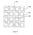
- FIG. 7 shows a diagram of a core 700 having a rectangular design in accordance with the invention.
- the center portion 710 has a grid shape, which can be considered an extension of the plus-shaped center portion 110 of the core 100 of FIGS. 1 and 2.
- the structure of core 700 may be derived by replicating the core of FIG. 2 three times. The number of primaries and secondaries on the posts determine the number of cells. If each post of core 700 is wound with two primaries and two secondaries, a sixteen cell structure results.
- each post of core 700 is wound with four primaries and four secondaries, then posts 720 on the corners will still share with two neighbors, but posts 730 on the edges will share with three neighbors and posts 740 on the interior will share with four neighbors—resulting in a 24 cell structure.
- the core may have other shapes besides square and circle.
- the desired number of cells may be used to determine the shape.
- the shape may be rectangular, hexagonal, trapezoidal, oval, T-shaped, L-shaped and other regular and irregular shapes.
- a core in accordance with the invention may be viewed as a combination of typical E-cores.
- the E-core may be considered an elementary cell, and a core of the invention may be derived by integrating multiple such cells with a shared center portion. By replicating elementary cells, one can develop higher current modules without compromising performance and power density.
- this cellular structure enables the development of novel interleaving schemes to reduce switching ripple in inductor current and output voltage. It also facilitates higher integration for multiple output, power supplies with integrated magnetics.
- the invention is applicable to both symmetrical and asymmetrical control schemes.
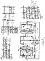
- FIG. 8 A power converter topology with reduces output voltage ripple is shown in FIG. 8. At least two CDRs are preferably wound on a common core—preferably on the novel core described above and shown at the bottom of FIG. 8—but could also be implemented, for example, on respective E-cores.
- the converter shown in FIG. 8 is a DC-DC converter which includes two interleaved half-bridge, isolated CDRS, though the concept is extendible to converters made from more or less than two CDRs.
- the converter is operated by applying AC drive voltages to respective primary windings.
- the drive voltages could be generated independently and applied to the primary windings, such that the present converter operates as an AC-DC converter. More typically, however, the present converter would be employed as a DC-DC converter, in which case the AC drive voltages are produced with a DC-AC converter such as DC-AC converter 800 shown in FIG. 8.
- a DC input voltage is connected across a first series-connected pair of switches S 11 and S 12 , and across a second series-connected pair of switches S 21 and S 22 . Switches S 11 and S 12 are connected together at a node 802 , and switches S 21 and S 22 are connected together at a node 804 .
- Switches S 11 , S 12 , S 21 and S 22 are preferably FETs, each of which has a parasitic diode (D 1 , D 2 , D 3 , D 4 ) connected across it.
- the DC input voltage is also connected across a pair of capacitors C 1 and C 2 , which are connected together at a common node 806 .
- Switches S 11 , S 12 , S 21 and S 22 are operated with a control circuit 808 to generate a first drive voltage V p1 between nodes 802 and 806 , and a second drive voltage V p2 between nodes 804 and 806 .
- the first CDR comprises two series-connected primary windings 810 and 812 , which are connected across nodes 802 and 806 and thus are driven with first drive voltage V p1 .
- a pair of secondary windings 814 and 816 are connected together at an output node 818 , and are magnetically coupled to primary windings 810 and 812 , respectively.
- a pair of series-connected switches SR 11 and SR 12 are connected in parallel with secondary windings 814 and 816 , respectively; switches SR 11 and SR 12 are connected together at a common node 820 .
- the second CDR comprises two series-connected primary windings 822 and 824 , which are connected across nodes 804 and 806 and thus are driven with second drive voltage V p2 .
- a pair of secondary windings 826 and 828 are connected together at output node 818 , and are magnetically coupled to primary windings 822 and 824 , respectively.
- a pair of series-connected switches SR 21 and SR 22 are connected in parallel with secondary windings 826 and 828 , respectively; switches SR 21 and SR 22 are connected together at common node 820 .
- Switches SR 11 , SR 12 , SR 21 and SR 22 are preferably FETs, each of which has a respective parasitic diode (D 5 , D 6 , D 7 and D 8 ) connected across it as shown in FIG. 8; alternatively, SR 11 , SR 12 , SR 21 and SR 22 could be implemented with just diodes oriented in the same way as D 5 , D 6 , D 7 and D 8 .
- a filter capacitor C 3 is connected between output node 818 and common node 820 .
- a load 830 would also be connected between output node 818 and common node 820 .
- each primary and secondary pair would be wound on a respective one of the outer posts.
- windings 810 and 814 would be on the outer post labeled “11”
- windings 812 and 816 would be on the outer post labeled “12”
- windings 822 and 826 would be on the outer post labeled “21”
- windings 824 and 828 would be on the outer post labeled “22”.
- windings 810 / 814 and 812 / 816 would be on respective outer posts of one of the E-cores
- windings 822 / 826 and 824 / 828 would be on respective outer posts of the other E-core.
- the AC drive voltages are generated in accordance with the symmetric modulation scheme.
- the drive voltages applied to respective CDRs are phase-shifted with respect to each other, by T s /(2*N), where T s is the drive voltages' switching period and N is the number of CDRs.
- control circuit 808 operates switches S 11 , S 12 , S 21 and S 22 such that the drive voltages V p1 and V p2 are phase-shifted by one-fourth the switching period T s , which ensures that the rectified output currents of the two CDRs are interleaved.
- Control circuit 808 also provides the signals needed to operate converter switches SR 11 , SR 12 , SR 21 and SR 22 .
- FIGS. 9 - 13 The operational stages of the exemplary DC-DC converter shown in FIG. 8 are illustrated in FIGS. 9 - 13 .
- a timing diagram for drive voltages V p1 and V p2 is shown at the top of each of these figures.
- a timing diagram is shown in FIG. 14 which depicts drive voltages V p1 and V p2 , the currents conducted to load 830 via switches SR 11 , SR 12 , SR 21 and SR 22 (i SR11 , i SR12 , i SR21 and i SR22 , respectively) , the ripple component for the total current provided to the load (i total ), and the output voltage ripple (V o ) (DC component not shown), for one switching period T s .
- the timing diagrams illustrate how the AC drive voltages are phase-shifted by one-fourth the switching period T s .
- D the percentage of time that the current in any given winding is increasing
- D*T s the percentage of time that the current in any given winding is increasing
- N 2 as in this example, there are four distinct “power transfer” periods in each switching period.
- the power transfer periods are denoted as PT 11 , PT 12 , PT 21 and PT 22 , and the switches which are closed by control circuit 808 during each power transfer period are listed on the appropriate timing diagram.
- a switch When a switch is closed, it is shown on the schematic as a solid, bold line.
- Direction of current flow is indicated with arrows.
- the operation of the following pairs of switches is complementary—i.e., when one is on, the other is off: SR 11 , and S 12 , SR 12 and S 11 , SR 21 and S 22 , SR 22 and S 21 .
- the converter is arranged such that SR 11 conducts when the voltage across SR 12 is positive with respect to common node 820 and V p1 is positive, and SR 12 conducts when the voltage across SR 11 is positive with respect to common node 820 and V p1 is negative.
- SR 21 conducts when the voltage across SR 22 is positive with respect to common node 820 and V p2 is positive, and SR 22 conducts when the voltage across SR 21 is positive with respect to common node 820 and V p2 is negative.
- FIG. 9 illustrates the PT 11 , stage of operation, when V p1 is positive and V p2 is zero. Switches S 11 , SR 11 , SR 21 and SR 22 are closed. When so arranged, V p1 is applied across the primary windings 810 , 812 of CDR-I and power is transferred from the primary to the secondary of CDR-I. Switch SR 11 carries the reflected primary current from winding 810 . This current includes the freewheeling current due to the decaying flux in the outer post with windings 810 and 814 , and the charging current that causes the flux to rise in the outer post with windings 816 and 812 . No current flows through secondary winding 816 as SR 12 is off. Since both S 21 and S 22 are off, no voltage is applied across the primary windings 822 , 824 of CDR-II, and thus the secondary currents of CDR-II freewheel through SR 21 and SR 22 .
- FIG. 10 shows the PT 21 stage of operation, when V p2 is positive and V p1 is zero. Switches S 21 , SR 11 , SR 12 and SR 21 are closed. When so arranged, V p2 is applied across the primary windings 822 , 824 of CDR-II and power is transferred from the primary to the secondary of CDR-II. Switch SR 21 carries the reflected primary current from winding 822 . This current includes the freewheeling current due to the decaying flux in the outer post with windings 822 and 826 , and the charging current that causes the flux to rise in the outer post with windings 824 and 828 . No current flows through secondary winding 828 as SR 22 is off. Since both S 11 and S 12 are off, no voltage is applied across the primary windings 810 , 812 of CDR-I, and thus the secondary currents of CDR-II freewheel through SR 11 and SR 12 .
- FIG. 11 shows the PT 12 stage of operation, when V p1 is negative and V p2 is zero.
- Switches S 12 , SR 12 , SR 21 and SR 22 are closed.
- ⁇ V p1 is applied across the primary windings 810 , 812 of CDR-I and power is transferred from the primary to the secondary of CDR-I.
- Switch SR 12 carries the reflected primary current from winding 812 .
- This current includes the freewheeling current due to the decaying flux in the outer post with windings 812 and 816 , and the charging current that causes the flux to rise in the outer post with windings 810 and 814 .
- FIG. 12 shows the PT 22 stage of operation, when Vp 2 is negative and V p1 is zero.
- Switches S 22 , SR 11 , SR 12 and SR 22 are closed.
- ⁇ Vp 2 is applied across the primary windings 822 , 824 of CDR-II and power is transferred from the primary to the secondary of CDR-II.
- Switch SR 22 carries the reflected primary current from winding 824 .
- This current includes the freewheeling current due to the decaying flux in the outer post with windings 824 and 828 , and the charging current that causes the flux to rise in the outer post with windings 822 and 826 .
- FIG. 13 depicts the operation of the converter if both drive voltages are zero.
- no power is transferred from the primary windings to the secondary windings, as all of the DC-AC converter switches (S 11 , S 12 , S 21 and S 22 ) are open.
- switches SR 11 , SR 12 , SR 21 and SR 22 are closed, allowing the secondary currents of CDR-I to freewheel through SR 11 and SR 12 , and the secondary currents of CDR-II to freewheel through SR 21 and SR 22 .
- this “freewheeling” stage occurs between every power transfer stage if and only if D*T s ⁇ T s /4.
- D*T s be less than T s /4. If D*T s >T s /4, the V p1 and V p2 waveforms and the power transfer periods will overlap, and there will be no period during which all the secondary currents are freewheeling.
- the interleaved currents produced with a DC-DC converter as described above results in reduced output current and output voltage ripple when compared with a single CDR configuration, making the present design well-suited to low voltage, high current DC-DC converter applications such as personal computer power supply.
- the present converter enables the size, cost, RMS loss and capacitance of the converter's filter capacitor to be smaller for a given ripple requirement.
- the present DC-DC converter topology is preferably implemented on the novel core structure described above.
- the invention is not limited to use with such a core structure.
- the first and second CDRs could be implemented on separate E-cores.
- the DC-AC converter 800 shown in FIGS. 8 - 13 is merely exemplary. It is only required that AC drive voltages as described herein be applied to at least two interleaved half-bridge, isolated CDRs.
- switches SR 11 , SR 1 2 , SR 21 and SR 22 be implemented with respective FET/diode circuits as shown in FIGS. 8 - 13 .
- each of these circuits could be replaced with respective diodes, oriented to conduct current from common node 820 to its secondary winding when forward-biased, and to block the flow of current between the secondary winding and common node 820 otherwise.
- MOSFETs should be used instead of diodes, in order to prevent loss of output voltage due to the diodes' high forward voltage drop. The diodes' high forward voltage drop also reduces efficiency due to large secondary currents.
- the invention is not limited to use with two CDRs which generate four interleaved currents.
- the concept can be easily adapted to converters which generate more or less than four interleaved currents, by, for example, reducing the number of cells to two, or increasing the number of cells to more than four.
- four interleaved currents there are three such duty cycle values. This is illustrated for various values of N in the graph shown in FIG. 15.
Landscapes
- Engineering & Computer Science (AREA)
- Power Engineering (AREA)
- Dc-Dc Converters (AREA)
Abstract
Description
- This application is a continuation-in-part of application Ser. No. 10/126,477, filed Apr. 18, 2002.
- A portion of the disclosure of this patent document contains material which is subject to copyright protection. This patent document may show and/or describe matter which is or may become trade dress of the owner. The copyright and trade dress owner has no objection to the facsimile reproduction by any one of the patent disclosure as it appears in the Patent and Trademark Office patent files or records, but otherwise reserves all copyright and trade dress rights whatsoever.
- [0003] The United States Government has rights in this invention pursuant to Contract No. 48803-8101 (RC) and 44104-8901 (Govt.) between the United States Department of Defense, Office of Naval Research and Rockwell Scientific Co.
- 1. Field of the Invention
- This invention relates to the field of DC-DC converters, and particularly to core structures and converter topologies which achieve small output voltage ripple.
- 2. Description of the Related Art
- Power converters are key components in many military and commercial systems and they often govern size and performance. Power density, efficiency and reliability are key characteristics used to evaluate the characteristics of power converters. Transformers and inductors used within these power converters may be large and bulky and often limit their efficiency, power density and reliability.
- The electromagnetic theory of operation of inductors and transformers is well known. The general concepts for combining magnetic functions of inductors and transformers on a single magnetic core structure are also well known. Integrated transformer/inductor devices typically take advantage of a transformer's magnetizing inductance to combine the function of a transformer and the function of an inductor connected in parallel with the transformer's secondary winding on a single core structure. One type of well-known core is the E-core. An E-core has a cross-section that looks like the capital letter “E.” An E-core is typically disposed on its side, with the long part of the E at the bottom, forming a base. E-cores are commonly used in current doubler circuits.
- E-cores typically have one of two configurations—the EI-core or the EE-core. In the EI-core, a flat plate, the “I,” is disposed on top of the basic E-core. In the EE-core, two Es are put together, with the legs of the Es facing each other. The EI-core, the EE-core and other cores incorporating the E core structure are referred to generically as E-cores.
- E-cores are typically used for transformers and inductors, and a single E-core may be adapted for use as both a transformer and an inductor. In one typical design, both of the outer legs have a primary and a secondary winding. Voltage to the windings is typically switched so that only one outer leg at any given time is acting as a transformer. The device is said to have one or two switching periods during which the inductors charge, and a freewheeling period during which the inductors discharge. In devices having two switching phases, the circuitry provides for one outer leg to act as an inductor while the other outer leg is acting as a transformer. Because of their dual but time-separated nature, the outer legs are said to have a transformer phase and an inductor phase. E-cores can be isolated (without transformers) or non-isolated (with transformers). E-cores may also be used only as transformers.
- When an outer leg of an E-core is acting as an inductor, magnetic flux is stored in the core. Magnetic flux flows through the outer leg which is acting as an inductor, through the top, the base, and through the center leg of the E. To provide increased energy storage, there is typically an air gap between the center leg and the top. Because of the air gap, the center leg is therefore typically shorter than the outer legs. Inductance in an E-core is primarily determined by the area of the center leg. To obtain higher inductance, the area of the center leg is increased.
- One limitation on the area of the center leg is fringing flux. Like bright light from one room leaking under a door into a dark second room, flux from the air gap can spill onto the outer legs. Fringing flux causes current losses in the transformer of the other outer leg. One way to accommodate fringing flux is to place the windings on the outer legs a safe distance from the air gap. To do this, the outer legs may be far from the center leg, or the outer legs may be longer so that the windings may be positioned closer to the base and far enough from the air gap. These two solutions result in either a wider E-core or a taller E-core, both of which can be burdens on mechanical designs. Another way to reduce fringing is to increase the area of the air gap. Fringing varies inversely with the area of the air gap.
- Another problem with most E-cores arises from their inefficiency. In general, the energy losses come in the form of heat. This generated heat can become a significant problem, requiring cooling through fans, air flow and other means. The additional power and cooling needs create additional burdens on electronic and mechanical designs.
- Such cores are often used to provide a DC-DC converter. A DC voltage is first converted to one or more AC drive voltages that toggle at a particular switching frequency. The AC drive voltages are applied to the primary windings of one or more magnetic cores, inducing currents in the secondary windings which are rectified to provide a DC output voltage. This type of converter can provide a high output current with very high efficiency.
- However, the output voltage ripple inherent in such converters can be excessive, particularly when a low (<2 V) supply voltage is needed. Output ripple can be reduced by increasing switching frequency, but this can result in unacceptable switching losses. Another way to reduce output ripple is with the use of a large output capacitor. However, the space allotted for a converter's output capacitor is often very limited, and thus the use of a larger capacitor is impractical.
- A magnetic core structure and converter topology are presented which overcome the problems noted above, providing high currents with less output ripple, without the need for a large output capacitor.
- The new converter topology converts a DC voltage to N AC drive voltages suitable for driving N interleaved, half-bridge, isolated current doubler rectifiers (CDRs) in accordance with the symmetric modulation scheme. Each CDR is driven with a respective AC drive voltage and is arranged to provide two rectified output currents to an output node; each AC drive voltage has a switching period T s. The AC drive voltages are phase-shifted by Ts/(2*N), such that the rectified output currents of the N CDRs are interleaved.
- Each CDR preferably comprises first and second primary windings connected in series, and first and second secondary windings which are connected together at the output node, with the first and second secondary windings magnetically coupled to the first and second primary windings, respectively. The primary and secondary windings are preferably wound on a common core—preferably the novel core described herein. The AC drive voltages are applied across the series-connected first and second primary windings. A preferred embodiment comprises 2 CDRs arranged to produce four interleaved currents using phase-shifted AC drive voltages as described above. When so arranged, the output voltage ripple of the converter is significantly reduced, such that, when compared with prior art designs, the size, cost, RMS loss and capacitance of the output filter can be much smaller for a given ripple requirement.
- Further features and advantages of the invention will be apparent to those skilled in the art from the following detailed description, taken together with the accompanying drawings.
- FIG. 1 is an exploded side elevated view of a core having a rectangular design in accordance with the invention;
- FIG. 2 is a top view of the core of FIG. 1;
- FIG. 3 is a side view of the core of FIG. 1;
- FIG. 4A is a top view of a core having a radial design in accordance with the invention;
- FIG. 4B is a side view of the core of FIG. 4A;
- FIG. 5A is a diagram showing a winding arrangement and some electrical components for a power converting apparatus in accordance with the invention;
- FIG. 5B is a circuit diagram corresponding to FIG. 5A;
- FIG. 6 is a top view of a core having a radial design in accordance with the invention; and
- FIG. 7 is a top view of a core having a rectangular design in accordance with the invention.
- FIG. 8 is a schematic diagram of a DC-DC converter topology in accordance with the invention.
- FIG. 9 is a schematic and timing diagram illustrating the operation of the present DC-DC converter during a first power transfer stage.
- FIG. 10 is a schematic and timing diagram illustrating the operation of the present DC-DC converter during a second power transfer stage.
- FIG. 11 is a schematic and timing diagram illustrating the operation of the present DC-DC converter during a third power transfer stage.
- FIG. 12 is a schematic and timing diagram illustrating the operation of the present DC-DC converter during a fourth power transfer stage.
- FIG. 13 is a schematic and timing diagram illustrating the operation of the present DC-DC converter during a freewheeling period.
- FIG. 14 is a timing diagram illustrating the operation of the present DC-DC converter for one switching period.
- FIG. 15 is a graph plotting current ripple vs. duty cycle for various numbers of interleaved currents.
- Throughout this description, the embodiments and examples shown should be considered as exemplars, rather than limitations on the apparatus and methods of the present invention.
- A core in accordance with the invention is useful in power modules and power converters. These power modules and power converters are well suited for low voltage, high current DC-DC converter applications. A core in accordance with the invention may have ultra-low profile magnetics, resulting in better utilization, higher inductance, improved efficiency and lower temperature. In typical E-cores, increased compactness results in decreased efficiency. In contrast, in a core of the invention, increased compactness may result in increased efficiency. Improved efficiency is an unexpected benefit of the invention.
- Principals of the invention are described below with respect to a half-bridge current doubler rectifier application. The invention is, however, applicable to a wide variety of DC-DC converter topologies and control algorithms. The core of the invention may also be useful in other types of power converters and modules, such as AC-AC and AC-DC. The cellular structure also enables the use of interleaving with multi-phase DC-DC converters to further reduce the current and voltage ripple and higher integration levels for multiple output DC-DC converters with integrated magnetics
- Referring now to FIGS. 1 and 2, there are shown two views of a
core 100 having a square design in accordance with the invention. Thecore 100 comprises abase 180, acenter portion 110,plural posts base 180, theposts center portion 110 may be produced as an integrated unit. Alternatively, some or all of theseparts core 100 may be formed of a single material. Alternatively, the materials of the separate components may be different and varied. The materials may be magnetic, such as ferrite, 3F3, powdered iron, nickel-iron alloys, or non-magnetic, or composite. - Whereas the base of a typical E-core has a linear shape, the
base 180 ofcore 100 has a square shape, with the fourposts posts top region 181 of thebase 180.Post 120 is disposed at the intersection ofouter edges Post 130 is disposed at the intersection ofouter edges Post 140 is disposed at the intersection ofouter edges Post 150 is disposed at the intersection ofouter edges base 180 is planar and thetop region 181 is flat where exposed, though these configurations are not required. - The
center portion 110 is also disposed on thetop region 181 of thebase 180. Thecenter portion 110 includeslegs posts Leg 112 is disposed betweenposts posts Leg 114 is disposed betweenposts Leg 115 is disposed betweenposts legs posts core 100 of FIGS. 1 and 2, thecenter portion 110 has a plus shape. - The
legs posts window 172 betweenpost 120 andcenter legs window 173 betweenpost 130 andcenter legs 112, 113. There is awindow 174 betweenpost 140 andcenter legs 113, 114. There is awindow 175 betweenpost 150 andcenter legs - The top 160 of
core 100 comprises a flat plate, similar to the top plate of an EI-core. However, a top in accordance with the invention need not be flat or plate-like, may be similar to that of an EE-core, and its shape may be adapted for the desired characteristics of the core. - Referring now to FIG. 3, there is shown a side view of the
core 100. In this view, thecore 100 looks like a typical E-core. In this view, anair gap 310 is apparent. Theair gap 310 is defined by the top 160 and thecenter portion 110. The height ofleg 115 is exaggerated in this view to make theair gap 310 larger and therefore more apparent. Theair gap 310 extends the entire space between thecenter portion 110 and the top 160—above all of thelegs - The view of FIG. 3 demonstrates the cellular nature of a core of the present invention. As used herein, a “cell” comprises two posts, the base and the center portion. Although two posts in part define a cell, windings on these posts and their electrical connections provide further definition of a cell. The number of primary and secondary windings on a given post is selected based in part upon the number of cells which are desired to share the post.
- The
core 100 may be used in a four cell structure. The combination of the twoposts center portion 110 and the base 180 may be used in one cell of thecore 100. The view taken from any of the foursides core 100 has the same appearance. Thus, the four cells ofcore 100 may be comprised of thecenter portion 110, thebase 180 and any two adjacent posts: post 120+post 150, post 120+post 130, post 130+post 140, or post 140+post 150. Whether such a combination is a cell, however, depends on the windings on each post. - One of the benefits of the core of the present invention is the presence of a shorter air gap than would be found in a comparable typical E-core or collection of E-cores. Whereas a typical E-core has a center leg between the two outer legs, the core of the invention has a center portion which may be considerably larger in comparison. The larger center portion may result in a shorter air gap. The shorter air gap has reduced fringing flux, meaning that the core may be more compact. In use, a power converter or power module of the invention should be considerably more efficient than a collection of E-cores providing comparable outputs. Thus, power consumption is reduced, heat losses are reduced, cooling requirements are reduced, and overall size requirements are reduced.
- Referring now to FIG. 4A, there is shown a top view of a
core 400 having a radial design in accordance with the invention. Theradial core 400 is similar to therectangular core 100 of FIG. 1. Thecore 400 includes abase 480,center portion 410,posts windows base 480 is round and theposts center portion 410 has a roundcentral portion 411Legs central portion 411. - The
core 400 has a cellular structure. Referring now to FIG. 4B, there is shown a side view of thecore 400. From the side, thecore 400 has substantially the same appearance as therectangular core 100 shown in FIG. 3. In FIG. 4B, the visible cell comprisesposts center portion 410 and thebase 480. Thecore 400 has three more cells, also comprised of thecenter portion 410, thebase 480, and: post 420+post 430, post 440+post 450, and post 420+post 450. - The desired transformer and inductor behavior, as well as cost and mechanical constraints, determine dimensions of the core, posts, legs, windows and air gap. Although the
cores - Although some center portion must be included in a core, the legs may be omitted. The legs improve performance of the power conducting device by giving a shorter or more direct path to the center area. The legs also contribute to the larger area of the center portion and the larger area of the air gap.
- Because of the large center portion of a core of the invention, very high inductance can be obtained from a smaller device. The size and shape of the center portion may be determined from the maximum flux density of the material and the total load current. How far the legs extend to, along side and past the posts may be determined from many factors, including performance, cost, and ease of manufacturing.
- FIG. 5A is a diagram showing a winding arrangement, wiring and some components for a four cell
power converting apparatus 500 in accordance with the invention. A center portion is not shown in FIG. 5. The winding arrangement of FIG. 5A is compatible with both therectangular core 100 of FIG. 1 and theradial core 400 of FIG. 4. Thepower converting apparatus 500 includesposts posts - In the four
cell core 500 of FIG. 5, theposts cell comprising posts posts - Referring now to FIG. 5B, there is shown a circuit diagram corresponding to the diagram of FIG. 5A. A typical E-core is used in a current doubler circuit. The circuit of FIG. 5B is a current quadrupler.
- FIG. 6 shows a diagram of another
core 600 having a radial design.Center portion 610 has around center 611 andradial legs core 600 may be derived from the four cell structure of FIG. 3 by adding additional sectors (posts, legs and windows). Like the radial four cell structure, the radial eight cell structure has two primary windings and two secondary windings on each post. - FIG. 7 shows a diagram of a core 700 having a rectangular design in accordance with the invention. In FIG. 7, the
center portion 710 has a grid shape, which can be considered an extension of the plus-shapedcenter portion 110 of thecore 100 of FIGS. 1 and 2. The structure of core 700 may be derived by replicating the core of FIG. 2 three times. The number of primaries and secondaries on the posts determine the number of cells. If each post of core 700 is wound with two primaries and two secondaries, a sixteen cell structure results. But if each post of core 700 is wound with four primaries and four secondaries, then posts 720 on the corners will still share with two neighbors, but posts 730 on the edges will share with three neighbors andposts 740 on the interior will share with four neighbors—resulting in a 24 cell structure. - The core may have other shapes besides square and circle. The desired number of cells may be used to determine the shape. The shape may be rectangular, hexagonal, trapezoidal, oval, T-shaped, L-shaped and other regular and irregular shapes.
- A core in accordance with the invention may be viewed as a combination of typical E-cores. In this way, the E-core may be considered an elementary cell, and a core of the invention may be derived by integrating multiple such cells with a shared center portion. By replicating elementary cells, one can develop higher current modules without compromising performance and power density.
- As can be seen, this cellular structure enables the development of novel interleaving schemes to reduce switching ripple in inductor current and output voltage. It also facilitates higher integration for multiple output, power supplies with integrated magnetics. The invention is applicable to both symmetrical and asymmetrical control schemes.
- A power converter topology with reduces output voltage ripple is shown in FIG. 8. At least two CDRs are preferably wound on a common core—preferably on the novel core described above and shown at the bottom of FIG. 8—but could also be implemented, for example, on respective E-cores. The converter shown in FIG. 8 is a DC-DC converter which includes two interleaved half-bridge, isolated CDRS, though the concept is extendible to converters made from more or less than two CDRs.
- The converter is operated by applying AC drive voltages to respective primary windings. The drive voltages could be generated independently and applied to the primary windings, such that the present converter operates as an AC-DC converter. More typically, however, the present converter would be employed as a DC-DC converter, in which case the AC drive voltages are produced with a DC-AC converter such as DC-
AC converter 800 shown in FIG. 8. A DC input voltage is connected across a first series-connected pair of switches S11 and S12, and across a second series-connected pair of switches S21 and S22. Switches S11 and S12 are connected together at anode 802, and switches S21 and S22 are connected together at anode 804. Switches S11, S12, S21 and S22 are preferably FETs, each of which has a parasitic diode (D1, D2, D3, D4) connected across it. The DC input voltage is also connected across a pair of capacitors C1 and C2, which are connected together at acommon node 806. Switches S11, S12, S21 and S22 are operated with acontrol circuit 808 to generate a first drive voltage Vp1 betweennodes nodes - The first CDR, “CDR-I”, comprises two series-connected
primary windings nodes secondary windings output node 818, and are magnetically coupled toprimary windings secondary windings common node 820. - Similarly, the second CDR, “CDR-II”, comprises two series-connected
primary windings nodes secondary windings output node 818, and are magnetically coupled toprimary windings secondary windings common node 820. - Switches SR 11, SR12, SR21 and SR22 are preferably FETs, each of which has a respective parasitic diode (D5, D6, D7 and D8) connected across it as shown in FIG. 8; alternatively, SR11, SR12, SR21 and SR22 could be implemented with just diodes oriented in the same way as D5, D6, D7 and D8. A filter capacitor C3 is connected between
output node 818 andcommon node 820. Aload 830 would also be connected betweenoutput node 818 andcommon node 820. - If wound on the novel core shown at the bottom of FIG. 8, each primary and secondary pair would be wound on a respective one of the outer posts. For example,
windings windings windings windings windings 810/814 and 812/816 would be on respective outer posts of one of the E-cores, andwindings 822/826 and 824/828 would be on respective outer posts of the other E-core. - The AC drive voltages are generated in accordance with the symmetric modulation scheme. In accordance with the present invention, the drive voltages applied to respective CDRs are phase-shifted with respect to each other, by T s/(2*N), where Ts is the drive voltages' switching period and N is the number of CDRs. For the converter shown in FIG. 8, with N=2,
control circuit 808 operates switches S11, S12, S21 and S22 such that the drive voltages Vp1 and Vp2 are phase-shifted by one-fourth the switching period Ts, which ensures that the rectified output currents of the two CDRs are interleaved.Control circuit 808 also provides the signals needed to operate converter switches SR11, SR12, SR21 and SR22. - The operational stages of the exemplary DC-DC converter shown in FIG. 8 are illustrated in FIGS. 9-13. A timing diagram for drive voltages Vp1 and Vp2 is shown at the top of each of these figures. A timing diagram is shown in FIG. 14 which depicts drive voltages Vp1 and Vp2, the currents conducted to load 830 via switches SR11, SR12, SR21 and SR22 (iSR11, iSR12, iSR21 and iSR22, respectively) , the ripple component for the total current provided to the load (itotal), and the output voltage ripple (Vo) (DC component not shown), for one switching period Ts.
- The timing diagrams illustrate how the AC drive voltages are phase-shifted by one-fourth the switching period T s. The width of each pulse is determined by the converter's duty cycle D(=the percentage of time that the current in any given winding is increasing), and is given by D*Ts. When N=2 as in this example, there are four distinct “power transfer” periods in each switching period. The power transfer periods are denoted as PT11, PT12, PT21 and PT22, and the switches which are closed by
control circuit 808 during each power transfer period are listed on the appropriate timing diagram. When a switch is closed, it is shown on the schematic as a solid, bold line. Direction of current flow is indicated with arrows. When arranged as shown in FIGS. 8-13, the operation of the following pairs of switches is complementary—i.e., when one is on, the other is off: SR11, and S12, SR12 and S11, SR21 and S22, SR22 and S21. The converter is arranged such that SR11 conducts when the voltage across SR12 is positive with respect tocommon node 820 and Vp1 is positive, and SR12 conducts when the voltage across SR11 is positive with respect tocommon node 820 and Vp1 is negative. Similarly, SR21 conducts when the voltage across SR22 is positive with respect tocommon node 820 and Vp2 is positive, and SR22 conducts when the voltage across SR21 is positive with respect tocommon node 820 and Vp2 is negative. - FIG. 9 illustrates the PT 11, stage of operation, when Vp1 is positive and Vp2 is zero. Switches S11, SR11, SR21 and SR22 are closed. When so arranged, Vp1 is applied across the
primary windings windings windings primary windings - FIG. 10 shows the PT 21 stage of operation, when Vp2 is positive and Vp1 is zero. Switches S21, SR11, SR12 and SR21 are closed. When so arranged, Vp2 is applied across the
primary windings windings windings primary windings - FIG. 11 shows the PT 12 stage of operation, when Vp1 is negative and Vp2 is zero. Switches S12, SR12, SR21 and SR22 are closed. When so arranged, −Vp1 is applied across the
primary windings windings windings primary windings - FIG. 12 shows the PT 22 stage of operation, when Vp2 is negative and Vp1 is zero. Switches S22, SR11, SR12 and SR22 are closed. When so arranged, −Vp2 is applied across the
primary windings windings windings primary windings - FIG. 13 depicts the operation of the converter if both drive voltages are zero. Here, no power is transferred from the primary windings to the secondary windings, as all of the DC-AC converter switches (S 11, S12, S21 and S22) are open. However, switches SR11, SR12, SR21 and SR22 are closed, allowing the secondary currents of CDR-I to freewheel through SR11 and SR12, and the secondary currents of CDR-II to freewheel through SR21 and SR22. Note that this “freewheeling” stage occurs between every power transfer stage if and only if D*Ts<Ts/4.
- Note that it is not essential that D*T s be less than Ts/4. If D*Ts>Ts/4, the Vp1 and Vp2 waveforms and the power transfer periods will overlap, and there will be no period during which all the secondary currents are freewheeling.
- Referring to FIG. 14, it can be seen that the interleaved currents produced with a DC-DC converter as described above results in reduced output current and output voltage ripple when compared with a single CDR configuration, making the present design well-suited to low voltage, high current DC-DC converter applications such as personal computer power supply. In addition, when compared with prior art designs, the present converter enables the size, cost, RMS loss and capacitance of the converter's filter capacitor to be smaller for a given ripple requirement.
- As noted above, the present DC-DC converter topology is preferably implemented on the novel core structure described above. However, the invention is not limited to use with such a core structure. For example, the first and second CDRs could be implemented on separate E-cores.
- The integration of two CDRs on the novel core structure described above results in magnetic coupling between the outer posts of the core. However, the magnetic coupling does not affect the interleaving of the currents from the two CDRs. The symmetric voltages applied to the primary windings of the two CDRs define the variation of the fluxes in the outer legs of the core structure. Since the primary voltages are phase-shifted from each other by a fixed fraction of the switching time period, the outer post fluxes (equal to the integral of the voltage) are also phase-shifted and interleave as they enter the center leg. The currents flowing through the windings are determined by the fluxes and the reluctance matrix of the core structure. Due to the symmetry of the core structure, the secondary currents add up to the same sum as would be obtained when four triangular, phase-shifted currents are interleaved, even though their individual waveshapes are not triangular.
- The DC-
AC converter 800 shown in FIGS. 8-13 is merely exemplary. It is only required that AC drive voltages as described herein be applied to at least two interleaved half-bridge, isolated CDRs. - It is also not essential that switches SR 11, SR1 2, SR21 and SR22 be implemented with respective FET/diode circuits as shown in FIGS. 8-13. For example, each of these circuits could be replaced with respective diodes, oriented to conduct current from
common node 820 to its secondary winding when forward-biased, and to block the flow of current between the secondary winding andcommon node 820 otherwise. For low output voltages, MOSFETs should be used instead of diodes, in order to prevent loss of output voltage due to the diodes' high forward voltage drop. The diodes' high forward voltage drop also reduces efficiency due to large secondary currents. - The invention is not limited to use with two CDRs which generate four interleaved currents. The concept can be easily adapted to converters which generate more or less than four interleaved currents, by, for example, reducing the number of cells to two, or increasing the number of cells to more than four. When two interleaved currents are generated, there is one duty cycle value (D=0.5) for which the lowest possible interleaved current ripple will be realized. Similarly, when four interleaved currents are generated, there are three such duty cycle values. This is illustrated for various values of N in the graph shown in FIG. 15.
- While particular embodiments of the invention have been shown and described, numerous variations and alternate embodiments will occur to those skilled in the art. Accordingly, it is intended that the invention be limited only in terms of the appended claims.
Claims (21)
Priority Applications (4)
| Application Number | Priority Date | Filing Date | Title |
|---|---|---|---|
| US10/302,095 US7046523B2 (en) | 2002-04-18 | 2002-11-21 | Core structure and interleaved DC—DC converter topology |
| US10/922,067 US7280026B2 (en) | 2002-04-18 | 2004-08-19 | Extended E matrix integrated magnetics (MIM) core |
| US11/866,152 US7633369B2 (en) | 2002-04-18 | 2007-10-02 | Extended E matrix integrated magnetics (MIM) core |
| US12/637,470 US8134443B2 (en) | 2002-04-18 | 2009-12-14 | Extended E matrix integrated magnetics (MIM) core |
Applications Claiming Priority (2)
| Application Number | Priority Date | Filing Date | Title |
|---|---|---|---|
| US10/126,477 US6873237B2 (en) | 2002-04-18 | 2002-04-18 | Core structure |
| US10/302,095 US7046523B2 (en) | 2002-04-18 | 2002-11-21 | Core structure and interleaved DC—DC converter topology |
Related Parent Applications (1)
| Application Number | Title | Priority Date | Filing Date |
|---|---|---|---|
| US10/126,477 Continuation-In-Part US6873237B2 (en) | 2002-04-18 | 2002-04-18 | Core structure |
Related Child Applications (2)
| Application Number | Title | Priority Date | Filing Date |
|---|---|---|---|
| US10/126,477 Continuation-In-Part US6873237B2 (en) | 2002-04-18 | 2002-04-18 | Core structure |
| US10/922,067 Continuation-In-Part US7280026B2 (en) | 2002-04-18 | 2004-08-19 | Extended E matrix integrated magnetics (MIM) core |
Publications (2)
| Publication Number | Publication Date |
|---|---|
| US20030198067A1 true US20030198067A1 (en) | 2003-10-23 |
| US7046523B2 US7046523B2 (en) | 2006-05-16 |
Family
ID=34107136
Family Applications (1)
| Application Number | Title | Priority Date | Filing Date |
|---|---|---|---|
| US10/302,095 Expired - Lifetime US7046523B2 (en) | 2002-04-18 | 2002-11-21 | Core structure and interleaved DC—DC converter topology |
Country Status (1)
| Country | Link |
|---|---|
| US (1) | US7046523B2 (en) |
Cited By (63)
| Publication number | Priority date | Publication date | Assignee | Title |
|---|---|---|---|---|
| US20060226478A1 (en) * | 2005-03-29 | 2006-10-12 | Brar Berinder P S | Semiconductor device having a lateral channel and contacts on opposing surfaces thereof |
| US20060226477A1 (en) * | 2005-03-29 | 2006-10-12 | Brar Berinder P S | Substrate driven field-effect transistor |
| US20070045765A1 (en) * | 2005-08-25 | 2007-03-01 | Brar Berinder P | Semiconductor device having substrate-driven field-effect transistor and schottky diode and method of forming the same |
| US20070069286A1 (en) * | 2005-09-27 | 2007-03-29 | Brar Berinder P S | Semiconductor device having an interconnect with sloped walls and method of forming the same |
| US20070187717A1 (en) * | 2005-05-13 | 2007-08-16 | Coldwatt, Inc. | Semiconductor device having reduced on-resistance and method of forming the same |
| US7280026B2 (en) | 2002-04-18 | 2007-10-09 | Coldwatt, Inc. | Extended E matrix integrated magnetics (MIM) core |
| US7298118B2 (en) | 2005-02-23 | 2007-11-20 | Coldwatt, Inc. | Power converter employing a tapped inductor and integrated magnetics and method of operating the same |
| US20070296028A1 (en) * | 2006-06-21 | 2007-12-27 | Brar Berinder P S | Vertical Field-Effect Transistor and Method of Forming the Same |
| US20070298564A1 (en) * | 2006-06-21 | 2007-12-27 | Brar Berinder P S | Vertical Field-Effect Transistor and Method of Forming the Same |
| US7321283B2 (en) | 2004-08-19 | 2008-01-22 | Coldwatt, Inc. | Vertical winding structures for planar magnetic switched-mode power converters |
| US20080048173A1 (en) * | 2005-08-25 | 2008-02-28 | Sadaka Mariam G | Semiconductor Device Including a Lateral Field-Effect Transistor and Schottky Diode |
| US7339208B2 (en) | 2005-05-13 | 2008-03-04 | Coldwatt, Inc. | Semiconductor device having multiple lateral channels and method of forming the same |
| US20080067990A1 (en) * | 2006-09-19 | 2008-03-20 | Intersil Americas Inc. | Coupled-inductor assembly with partial winding |
| US7385375B2 (en) | 2005-02-23 | 2008-06-10 | Coldwatt, Inc. | Control circuit for a depletion mode switch and method of operating the same |
| US7417875B2 (en) | 2005-02-08 | 2008-08-26 | Coldwatt, Inc. | Power converter employing integrated magnetics with a current multiplier rectifier and method of operating the same |
| US7427910B2 (en) | 2004-08-19 | 2008-09-23 | Coldwatt, Inc. | Winding structure for efficient switch-mode power converters |
| US20080303495A1 (en) * | 2007-06-08 | 2008-12-11 | Intersil Americas Inc. | Power supply with a magnetically uncoupled phase and an odd number of magnetically coupled phases, and control for a power supply with magnetically coupled and magnetically uncoupled phases |
| US20090045785A1 (en) * | 2007-08-14 | 2009-02-19 | Intersil Americas Inc. | Sensing a phase-path current in a multiphase power supply such as a coupled-inductor power supply |
| US20090059546A1 (en) * | 2007-08-31 | 2009-03-05 | Intersil Americas Inc. | Stackable electronic component |
| US20090256535A1 (en) * | 2008-04-10 | 2009-10-15 | Intersil Americas Inc. | Varying operation of a voltage regulator, and components thereof, based upon load conditions |
| US7667986B2 (en) | 2006-12-01 | 2010-02-23 | Flextronics International Usa, Inc. | Power system with power converters having an adaptive controller |
| US7675758B2 (en) | 2006-12-01 | 2010-03-09 | Flextronics International Usa, Inc. | Power converter with an adaptive controller and method of operating the same |
| US7675759B2 (en) | 2006-12-01 | 2010-03-09 | Flextronics International Usa, Inc. | Power system with power converters having an adaptive controller |
| US7876191B2 (en) | 2005-02-23 | 2011-01-25 | Flextronics International Usa, Inc. | Power converter employing a tapped inductor and integrated magnetics and method of operating the same |
| US7889517B2 (en) | 2006-12-01 | 2011-02-15 | Flextronics International Usa, Inc. | Power system with power converters having an adaptive controller |
| US7906941B2 (en) | 2007-06-19 | 2011-03-15 | Flextronics International Usa, Inc. | System and method for estimating input power for a power processing circuit |
| US8125205B2 (en) | 2006-08-31 | 2012-02-28 | Flextronics International Usa, Inc. | Power converter employing regulators with a coupled inductor |
| US8415737B2 (en) | 2006-06-21 | 2013-04-09 | Flextronics International Usa, Inc. | Semiconductor device with a pillar region and method of forming the same |
| US8502520B2 (en) | 2007-03-14 | 2013-08-06 | Flextronics International Usa, Inc | Isolated power converter |
| US8514593B2 (en) | 2009-06-17 | 2013-08-20 | Power Systems Technologies, Ltd. | Power converter employing a variable switching frequency and a magnetic device with a non-uniform gap |
| US8520414B2 (en) | 2009-01-19 | 2013-08-27 | Power Systems Technologies, Ltd. | Controller for a power converter |
| US8520420B2 (en) | 2009-12-18 | 2013-08-27 | Power Systems Technologies, Ltd. | Controller for modifying dead time between switches in a power converter |
| US8638578B2 (en) | 2009-08-14 | 2014-01-28 | Power System Technologies, Ltd. | Power converter including a charge pump employable in a power adapter |
| US8643222B2 (en) | 2009-06-17 | 2014-02-04 | Power Systems Technologies Ltd | Power adapter employing a power reducer |
| US8767418B2 (en) | 2010-03-17 | 2014-07-01 | Power Systems Technologies Ltd. | Control system for a power converter and method of operating the same |
| US8773231B2 (en) * | 2012-03-09 | 2014-07-08 | Raytheon Company | Multiphase power converters involving controllable inductors |
| US8787043B2 (en) | 2010-01-22 | 2014-07-22 | Power Systems Technologies, Ltd. | Controller for a power converter and method of operating the same |
| US8792257B2 (en) | 2011-03-25 | 2014-07-29 | Power Systems Technologies, Ltd. | Power converter with reduced power dissipation |
| US8792256B2 (en) | 2012-01-27 | 2014-07-29 | Power Systems Technologies Ltd. | Controller for a switch and method of operating the same |
| KR101444865B1 (en) | 2013-08-22 | 2014-10-02 | 삼성중공업 주식회사 | Leg performance test device |
| US8963521B2 (en) | 2007-06-08 | 2015-02-24 | Intersil Americas LLC | Power supply with a magnetically uncoupled phase and an odd number of magnetically coupled phases, and control for a power supply with magnetically coupled and magnetically uncoupled phases |
| US8976549B2 (en) | 2009-12-03 | 2015-03-10 | Power Systems Technologies, Ltd. | Startup circuit including first and second Schmitt triggers and power converter employing the same |
| US20150070943A1 (en) * | 2013-09-06 | 2015-03-12 | The Regents Of The University Of Colorado | High efficiency zero-voltage switching (zvs) assistance circuit for power converter |
| US9019061B2 (en) | 2009-03-31 | 2015-04-28 | Power Systems Technologies, Ltd. | Magnetic device formed with U-shaped core pieces and power converter employing the same |
| US9077248B2 (en) | 2009-06-17 | 2015-07-07 | Power Systems Technologies Ltd | Start-up circuit for a power adapter |
| US9088216B2 (en) | 2009-01-19 | 2015-07-21 | Power Systems Technologies, Ltd. | Controller for a synchronous rectifier switch |
| US9099232B2 (en) | 2012-07-16 | 2015-08-04 | Power Systems Technologies Ltd. | Magnetic device and power converter employing the same |
| US9106130B2 (en) | 2012-07-16 | 2015-08-11 | Power Systems Technologies, Inc. | Magnetic device and power converter employing the same |
| WO2015158982A1 (en) | 2014-04-14 | 2015-10-22 | Valeo Equipements Electriques Moteur | Planar transformer of a resonance dc/dc converter, and corresponding converter |
| US9190898B2 (en) | 2012-07-06 | 2015-11-17 | Power Systems Technologies, Ltd | Controller for a power converter and method of operating the same |
| US9197132B2 (en) | 2006-12-01 | 2015-11-24 | Flextronics International Usa, Inc. | Power converter with an adaptive controller and method of operating the same |
| US9214264B2 (en) | 2012-07-16 | 2015-12-15 | Power Systems Technologies, Ltd. | Magnetic device and power converter employing the same |
| US9240712B2 (en) | 2012-12-13 | 2016-01-19 | Power Systems Technologies Ltd. | Controller including a common current-sense device for power switches of a power converter |
| US9246391B2 (en) | 2010-01-22 | 2016-01-26 | Power Systems Technologies Ltd. | Controller for providing a corrected signal to a sensed peak current through a circuit element of a power converter |
| US9263961B2 (en) | 2013-07-23 | 2016-02-16 | Raytheon Company | Wide input DC/DC resonant converter to control reactive power |
| US9300206B2 (en) | 2013-11-15 | 2016-03-29 | Power Systems Technologies Ltd. | Method for estimating power of a power converter |
| US9379629B2 (en) | 2012-07-16 | 2016-06-28 | Power Systems Technologies, Ltd. | Magnetic device and power converter employing the same |
| US20170154718A1 (en) * | 2015-11-30 | 2017-06-01 | Fanuc Corporation | Multi-phase reactor capable of obtaining constant inductance for each phase |
| US10008322B2 (en) | 2014-10-29 | 2018-06-26 | General Electric Company | Filter assembly and method |
| US20200350117A1 (en) * | 2019-05-02 | 2020-11-05 | Virginia Tech Intellectual Properties, Inc. | Magnetic integration of matrix transformer with controllable leakage inductance |
| CN114203414A (en) * | 2020-09-17 | 2022-03-18 | 群光电能科技股份有限公司 | Transformer device |
| US11749452B2 (en) * | 2020-03-10 | 2023-09-05 | Delta Electronics (Thailand) Public Company Limited | Leakage transformer |
| US11799384B2 (en) * | 2020-01-28 | 2023-10-24 | International Business Machines Corporation | Power converter with co-packaged secondary field effect transistors (FETs) |
Families Citing this family (8)
| Publication number | Priority date | Publication date | Assignee | Title |
|---|---|---|---|---|
| US8595041B2 (en) * | 2006-02-07 | 2013-11-26 | Sap Ag | Task responsibility system |
| JP5685815B2 (en) * | 2009-03-16 | 2015-03-18 | Tdk株式会社 | Transformer and switching power supply |
| JP5257204B2 (en) * | 2009-03-31 | 2013-08-07 | Tdk株式会社 | Switching power supply |
| US8339808B2 (en) | 2009-06-19 | 2012-12-25 | Tdk Corporation | Switching power supply unit |
| CN102714468A (en) * | 2010-10-06 | 2012-10-03 | 三菱电机株式会社 | Power supply device |
| US20140016369A1 (en) | 2012-07-16 | 2014-01-16 | Power Systems Technologies, Ltd. | Magnetic Device and Power Converter Employing the Same |
| US20160247627A1 (en) | 2015-02-24 | 2016-08-25 | Maxim Integrated Products, Inc. | Low-profile coupled inductors with leakage control |
| US10297379B2 (en) | 2016-03-11 | 2019-05-21 | Maxim Integrated Products, Inc. | Integrated transformers and coupled inductors and associated systems and methods |
Citations (12)
| Publication number | Priority date | Publication date | Assignee | Title |
|---|---|---|---|---|
| US4823249A (en) * | 1987-04-27 | 1989-04-18 | American Telephone And Telegraph Company At&T Bell Laboratories | High-frequency resonant power converter |
| US4899271A (en) * | 1987-07-22 | 1990-02-06 | Scanpower | Power supply circuit |
| US5132888A (en) * | 1991-01-07 | 1992-07-21 | Unisys Corporation | Interleaved bridge converter |
| US5291382A (en) * | 1991-04-10 | 1994-03-01 | Lambda Electronics Inc. | Pulse width modulated DC/DC converter with reduced ripple current coponent stress and zero voltage switching capability |
| US5305191A (en) * | 1992-04-20 | 1994-04-19 | At&T Bell Laboratories | Drive circuit for zero-voltage switching power converter with controlled power switch turn-on |
| US5335163A (en) * | 1990-11-14 | 1994-08-02 | Scanpower | Power supply circuit with integrated magnetic components |
| US5508903A (en) * | 1995-04-21 | 1996-04-16 | Alexndrov; Felix | Interleaved DC to DC flyback converters with reduced current and voltage stresses |
| US5555494A (en) * | 1993-09-13 | 1996-09-10 | Morris; George Q. | Magnetically integrated full wave DC to DC converter |
| US5784266A (en) * | 1996-06-14 | 1998-07-21 | Virginia Power Technologies, Inc | Single magnetic low loss high frequency converter |
| US6215290B1 (en) * | 1999-11-15 | 2001-04-10 | Semtech Corporation | Multi-phase and multi-module power supplies with balanced current between phases and modules |
| US6683797B2 (en) * | 2002-01-24 | 2004-01-27 | Tdk Corporation | Multi-stage DC—DC converter |
| US6765810B2 (en) * | 2002-08-02 | 2004-07-20 | Artesyn Technologies, Inc. | Full-wave coupled inductor power converter having synchronous rectifiers and two input switches that are simultaneously off for a time period of each switching cycle |
-
2002
- 2002-11-21 US US10/302,095 patent/US7046523B2/en not_active Expired - Lifetime
Patent Citations (12)
| Publication number | Priority date | Publication date | Assignee | Title |
|---|---|---|---|---|
| US4823249A (en) * | 1987-04-27 | 1989-04-18 | American Telephone And Telegraph Company At&T Bell Laboratories | High-frequency resonant power converter |
| US4899271A (en) * | 1987-07-22 | 1990-02-06 | Scanpower | Power supply circuit |
| US5335163A (en) * | 1990-11-14 | 1994-08-02 | Scanpower | Power supply circuit with integrated magnetic components |
| US5132888A (en) * | 1991-01-07 | 1992-07-21 | Unisys Corporation | Interleaved bridge converter |
| US5291382A (en) * | 1991-04-10 | 1994-03-01 | Lambda Electronics Inc. | Pulse width modulated DC/DC converter with reduced ripple current coponent stress and zero voltage switching capability |
| US5305191A (en) * | 1992-04-20 | 1994-04-19 | At&T Bell Laboratories | Drive circuit for zero-voltage switching power converter with controlled power switch turn-on |
| US5555494A (en) * | 1993-09-13 | 1996-09-10 | Morris; George Q. | Magnetically integrated full wave DC to DC converter |
| US5508903A (en) * | 1995-04-21 | 1996-04-16 | Alexndrov; Felix | Interleaved DC to DC flyback converters with reduced current and voltage stresses |
| US5784266A (en) * | 1996-06-14 | 1998-07-21 | Virginia Power Technologies, Inc | Single magnetic low loss high frequency converter |
| US6215290B1 (en) * | 1999-11-15 | 2001-04-10 | Semtech Corporation | Multi-phase and multi-module power supplies with balanced current between phases and modules |
| US6683797B2 (en) * | 2002-01-24 | 2004-01-27 | Tdk Corporation | Multi-stage DC—DC converter |
| US6765810B2 (en) * | 2002-08-02 | 2004-07-20 | Artesyn Technologies, Inc. | Full-wave coupled inductor power converter having synchronous rectifiers and two input switches that are simultaneously off for a time period of each switching cycle |
Cited By (98)
| Publication number | Priority date | Publication date | Assignee | Title |
|---|---|---|---|---|
| US7633369B2 (en) | 2002-04-18 | 2009-12-15 | Flextronics International Usa, Inc. | Extended E matrix integrated magnetics (MIM) core |
| US8134443B2 (en) | 2002-04-18 | 2012-03-13 | Flextronics International Usa, Inc. | Extended E matrix integrated magnetics (MIM) core |
| US7280026B2 (en) | 2002-04-18 | 2007-10-09 | Coldwatt, Inc. | Extended E matrix integrated magnetics (MIM) core |
| US7321283B2 (en) | 2004-08-19 | 2008-01-22 | Coldwatt, Inc. | Vertical winding structures for planar magnetic switched-mode power converters |
| US7554430B2 (en) | 2004-08-19 | 2009-06-30 | Flextronics International Usa, Inc. | Vertical winding structures for planar magnetic switched-mode power converters |
| US7427910B2 (en) | 2004-08-19 | 2008-09-23 | Coldwatt, Inc. | Winding structure for efficient switch-mode power converters |
| US7675764B2 (en) | 2005-02-08 | 2010-03-09 | Flextronics International Usa, Inc. | Power converter employing integrated magnetics with a current multiplier rectifier and method of operating the same |
| US7417875B2 (en) | 2005-02-08 | 2008-08-26 | Coldwatt, Inc. | Power converter employing integrated magnetics with a current multiplier rectifier and method of operating the same |
| US7876191B2 (en) | 2005-02-23 | 2011-01-25 | Flextronics International Usa, Inc. | Power converter employing a tapped inductor and integrated magnetics and method of operating the same |
| US7298118B2 (en) | 2005-02-23 | 2007-11-20 | Coldwatt, Inc. | Power converter employing a tapped inductor and integrated magnetics and method of operating the same |
| US7385375B2 (en) | 2005-02-23 | 2008-06-10 | Coldwatt, Inc. | Control circuit for a depletion mode switch and method of operating the same |
| US20060226478A1 (en) * | 2005-03-29 | 2006-10-12 | Brar Berinder P S | Semiconductor device having a lateral channel and contacts on opposing surfaces thereof |
| US7439556B2 (en) | 2005-03-29 | 2008-10-21 | Coldwatt, Inc. | Substrate driven field-effect transistor |
| US20070145417A1 (en) * | 2005-03-29 | 2007-06-28 | Brar Berinder P S | High voltage semiconductor device having a lateral channel and enhanced gate-to-drain separation |
| US7439557B2 (en) | 2005-03-29 | 2008-10-21 | Coldwatt, Inc. | Semiconductor device having a lateral channel and contacts on opposing surfaces thereof |
| US20060226477A1 (en) * | 2005-03-29 | 2006-10-12 | Brar Berinder P S | Substrate driven field-effect transistor |
| US20070187717A1 (en) * | 2005-05-13 | 2007-08-16 | Coldwatt, Inc. | Semiconductor device having reduced on-resistance and method of forming the same |
| US7339208B2 (en) | 2005-05-13 | 2008-03-04 | Coldwatt, Inc. | Semiconductor device having multiple lateral channels and method of forming the same |
| US7838905B2 (en) | 2005-05-13 | 2010-11-23 | Flextronics International Usa, Inc. | Semiconductor device having multiple lateral channels and method of forming the same |
| US7675090B2 (en) | 2005-05-13 | 2010-03-09 | Flextronics International Usa, Inc. | Semiconductor device having a contact on a buffer layer thereof and method of forming the same |
| US7285807B2 (en) | 2005-08-25 | 2007-10-23 | Coldwatt, Inc. | Semiconductor device having substrate-driven field-effect transistor and Schottky diode and method of forming the same |
| US20080048174A1 (en) * | 2005-08-25 | 2008-02-28 | Sadaka Mariam G | Semiconductor Device Including a Lateral Field-Effect Transistor and Schottky Diode |
| US7564074B2 (en) | 2005-08-25 | 2009-07-21 | Flextronics International Usa, Inc. | Semiconductor device including a lateral field-effect transistor and Schottky diode |
| US20080054304A1 (en) * | 2005-08-25 | 2008-03-06 | Sadaka Mariam G | Semiconductor Device Including a Lateral Field-Effect Transistor and Schottky Diode |
| US7642568B2 (en) | 2005-08-25 | 2010-01-05 | Flextronics International Usa, Inc. | Semiconductor device having substrate-driven field-effect transistor and Schottky diode and method of forming the same |
| US20070045765A1 (en) * | 2005-08-25 | 2007-03-01 | Brar Berinder P | Semiconductor device having substrate-driven field-effect transistor and schottky diode and method of forming the same |
| US7655963B2 (en) | 2005-08-25 | 2010-02-02 | Flextronics International Usa, Inc. | Semiconductor device including a lateral field-effect transistor and Schottky diode |
| US20080048173A1 (en) * | 2005-08-25 | 2008-02-28 | Sadaka Mariam G | Semiconductor Device Including a Lateral Field-Effect Transistor and Schottky Diode |
| US7504673B2 (en) | 2005-08-25 | 2009-03-17 | Flextronics International Usa, Inc. | Semiconductor device including a lateral field-effect transistor and Schottky diode |
| US20080048219A1 (en) * | 2005-08-25 | 2008-02-28 | Brar Berinder P S | Semiconductor Device Having Substrate-Driven Field-Effect Transistor and Schottky Diode and Method of Forming the Same |
| US7462891B2 (en) | 2005-09-27 | 2008-12-09 | Coldwatt, Inc. | Semiconductor device having an interconnect with sloped walls and method of forming the same |
| US20070069286A1 (en) * | 2005-09-27 | 2007-03-29 | Brar Berinder P S | Semiconductor device having an interconnect with sloped walls and method of forming the same |
| US20070298564A1 (en) * | 2006-06-21 | 2007-12-27 | Brar Berinder P S | Vertical Field-Effect Transistor and Method of Forming the Same |
| US7541640B2 (en) | 2006-06-21 | 2009-06-02 | Flextronics International Usa, Inc. | Vertical field-effect transistor and method of forming the same |
| US8415737B2 (en) | 2006-06-21 | 2013-04-09 | Flextronics International Usa, Inc. | Semiconductor device with a pillar region and method of forming the same |
| US20070296028A1 (en) * | 2006-06-21 | 2007-12-27 | Brar Berinder P S | Vertical Field-Effect Transistor and Method of Forming the Same |
| US7663183B2 (en) | 2006-06-21 | 2010-02-16 | Flextronics International Usa, Inc. | Vertical field-effect transistor and method of forming the same |
| US8125205B2 (en) | 2006-08-31 | 2012-02-28 | Flextronics International Usa, Inc. | Power converter employing regulators with a coupled inductor |
| US20080067990A1 (en) * | 2006-09-19 | 2008-03-20 | Intersil Americas Inc. | Coupled-inductor assembly with partial winding |
| US7667986B2 (en) | 2006-12-01 | 2010-02-23 | Flextronics International Usa, Inc. | Power system with power converters having an adaptive controller |
| US7675758B2 (en) | 2006-12-01 | 2010-03-09 | Flextronics International Usa, Inc. | Power converter with an adaptive controller and method of operating the same |
| US7675759B2 (en) | 2006-12-01 | 2010-03-09 | Flextronics International Usa, Inc. | Power system with power converters having an adaptive controller |
| US7889517B2 (en) | 2006-12-01 | 2011-02-15 | Flextronics International Usa, Inc. | Power system with power converters having an adaptive controller |
| US9197132B2 (en) | 2006-12-01 | 2015-11-24 | Flextronics International Usa, Inc. | Power converter with an adaptive controller and method of operating the same |
| US8477514B2 (en) | 2006-12-01 | 2013-07-02 | Flextronics International Usa, Inc. | Power system with power converters having an adaptive controller |
| US8502520B2 (en) | 2007-03-14 | 2013-08-06 | Flextronics International Usa, Inc | Isolated power converter |
| US8179116B2 (en) | 2007-06-08 | 2012-05-15 | Intersil Americas LLC | Inductor assembly having a core with magnetically isolated forms |
| US8570009B2 (en) | 2007-06-08 | 2013-10-29 | Intersil Americas Inc. | Power supply with a magnetically uncoupled phase and an odd number of magnetically coupled phases, and control for a power supply with magnetically coupled and magnetically uncoupled phases |
| US8963521B2 (en) | 2007-06-08 | 2015-02-24 | Intersil Americas LLC | Power supply with a magnetically uncoupled phase and an odd number of magnetically coupled phases, and control for a power supply with magnetically coupled and magnetically uncoupled phases |
| US20080315982A1 (en) * | 2007-06-08 | 2008-12-25 | Intersil Americas Inc. | Coupled-inductor core for unbalanced phase currents |
| US20080309299A1 (en) * | 2007-06-08 | 2008-12-18 | Intersil Americas Inc. | Inductor assembly having a core with magnetically isolated forms |
| US20080303495A1 (en) * | 2007-06-08 | 2008-12-11 | Intersil Americas Inc. | Power supply with a magnetically uncoupled phase and an odd number of magnetically coupled phases, and control for a power supply with magnetically coupled and magnetically uncoupled phases |
| US7906941B2 (en) | 2007-06-19 | 2011-03-15 | Flextronics International Usa, Inc. | System and method for estimating input power for a power processing circuit |
| US20090045785A1 (en) * | 2007-08-14 | 2009-02-19 | Intersil Americas Inc. | Sensing a phase-path current in a multiphase power supply such as a coupled-inductor power supply |
| US9602005B2 (en) | 2007-08-14 | 2017-03-21 | Intersil Americas LLC | Sensing a phase-path current in a coupled-inductor power supply |
| US8704500B2 (en) | 2007-08-14 | 2014-04-22 | Intersil Americas LLC | Sensing a phase-path current in a multiphase power supply such as a coupled-inductor power supply |
| US8320136B2 (en) | 2007-08-31 | 2012-11-27 | Intersil Americas Inc. | Stackable electronic component |
| US20090059546A1 (en) * | 2007-08-31 | 2009-03-05 | Intersil Americas Inc. | Stackable electronic component |
| USRE45773E1 (en) | 2008-04-10 | 2015-10-20 | Intersil Americas Inc. | Varying operation of a voltage regulator, and components thereof, based upon load conditions |
| US7898236B2 (en) | 2008-04-10 | 2011-03-01 | Intersil Americas Inc. | Varying operation of a voltage regulator, and components thereof, based upon load conditions |
| US20090256535A1 (en) * | 2008-04-10 | 2009-10-15 | Intersil Americas Inc. | Varying operation of a voltage regulator, and components thereof, based upon load conditions |
| US8125207B2 (en) | 2008-04-10 | 2012-02-28 | Intersil Americas Inc. | Varying operation of a voltage regulator, and components thereof, based upon load conditions |
| US20110062930A1 (en) * | 2008-04-10 | 2011-03-17 | Intersil Americas Inc. | Varying operation of a voltage regulator, and components thereof, based upon load conditions |
| US9088216B2 (en) | 2009-01-19 | 2015-07-21 | Power Systems Technologies, Ltd. | Controller for a synchronous rectifier switch |
| US8520414B2 (en) | 2009-01-19 | 2013-08-27 | Power Systems Technologies, Ltd. | Controller for a power converter |
| US9019061B2 (en) | 2009-03-31 | 2015-04-28 | Power Systems Technologies, Ltd. | Magnetic device formed with U-shaped core pieces and power converter employing the same |
| US8514593B2 (en) | 2009-06-17 | 2013-08-20 | Power Systems Technologies, Ltd. | Power converter employing a variable switching frequency and a magnetic device with a non-uniform gap |
| US9077248B2 (en) | 2009-06-17 | 2015-07-07 | Power Systems Technologies Ltd | Start-up circuit for a power adapter |
| US8643222B2 (en) | 2009-06-17 | 2014-02-04 | Power Systems Technologies Ltd | Power adapter employing a power reducer |
| US8638578B2 (en) | 2009-08-14 | 2014-01-28 | Power System Technologies, Ltd. | Power converter including a charge pump employable in a power adapter |
| US8976549B2 (en) | 2009-12-03 | 2015-03-10 | Power Systems Technologies, Ltd. | Startup circuit including first and second Schmitt triggers and power converter employing the same |
| US8520420B2 (en) | 2009-12-18 | 2013-08-27 | Power Systems Technologies, Ltd. | Controller for modifying dead time between switches in a power converter |
| US9246391B2 (en) | 2010-01-22 | 2016-01-26 | Power Systems Technologies Ltd. | Controller for providing a corrected signal to a sensed peak current through a circuit element of a power converter |
| US8787043B2 (en) | 2010-01-22 | 2014-07-22 | Power Systems Technologies, Ltd. | Controller for a power converter and method of operating the same |
| US8767418B2 (en) | 2010-03-17 | 2014-07-01 | Power Systems Technologies Ltd. | Control system for a power converter and method of operating the same |
| US8792257B2 (en) | 2011-03-25 | 2014-07-29 | Power Systems Technologies, Ltd. | Power converter with reduced power dissipation |
| US8792256B2 (en) | 2012-01-27 | 2014-07-29 | Power Systems Technologies Ltd. | Controller for a switch and method of operating the same |
| US8773231B2 (en) * | 2012-03-09 | 2014-07-08 | Raytheon Company | Multiphase power converters involving controllable inductors |
| US9190898B2 (en) | 2012-07-06 | 2015-11-17 | Power Systems Technologies, Ltd | Controller for a power converter and method of operating the same |
| US9099232B2 (en) | 2012-07-16 | 2015-08-04 | Power Systems Technologies Ltd. | Magnetic device and power converter employing the same |
| US9106130B2 (en) | 2012-07-16 | 2015-08-11 | Power Systems Technologies, Inc. | Magnetic device and power converter employing the same |
| US9379629B2 (en) | 2012-07-16 | 2016-06-28 | Power Systems Technologies, Ltd. | Magnetic device and power converter employing the same |
| US9214264B2 (en) | 2012-07-16 | 2015-12-15 | Power Systems Technologies, Ltd. | Magnetic device and power converter employing the same |
| US9240712B2 (en) | 2012-12-13 | 2016-01-19 | Power Systems Technologies Ltd. | Controller including a common current-sense device for power switches of a power converter |
| US9263961B2 (en) | 2013-07-23 | 2016-02-16 | Raytheon Company | Wide input DC/DC resonant converter to control reactive power |
| KR101444865B1 (en) | 2013-08-22 | 2014-10-02 | 삼성중공업 주식회사 | Leg performance test device |
| US20150070943A1 (en) * | 2013-09-06 | 2015-03-12 | The Regents Of The University Of Colorado | High efficiency zero-voltage switching (zvs) assistance circuit for power converter |
| US9407150B2 (en) * | 2013-09-06 | 2016-08-02 | Raytheon Company | High efficiency zero-voltage switching (ZVS) assistance circuit for power converter |
| US9300206B2 (en) | 2013-11-15 | 2016-03-29 | Power Systems Technologies Ltd. | Method for estimating power of a power converter |
| WO2015158982A1 (en) | 2014-04-14 | 2015-10-22 | Valeo Equipements Electriques Moteur | Planar transformer of a resonance dc/dc converter, and corresponding converter |
| US10008322B2 (en) | 2014-10-29 | 2018-06-26 | General Electric Company | Filter assembly and method |
| US20170154718A1 (en) * | 2015-11-30 | 2017-06-01 | Fanuc Corporation | Multi-phase reactor capable of obtaining constant inductance for each phase |
| US10373753B2 (en) * | 2015-11-30 | 2019-08-06 | Fanuc Corporation | Multi-phase reactor capable of obtaining constant inductance for each phase |
| US20200350117A1 (en) * | 2019-05-02 | 2020-11-05 | Virginia Tech Intellectual Properties, Inc. | Magnetic integration of matrix transformer with controllable leakage inductance |
| US12009146B2 (en) * | 2019-05-02 | 2024-06-11 | Virginia Tech Intellectual Properties, Inc. | Magnetic integration of matrix transformer with controllable leakage inductance |
| US11799384B2 (en) * | 2020-01-28 | 2023-10-24 | International Business Machines Corporation | Power converter with co-packaged secondary field effect transistors (FETs) |
| US11749452B2 (en) * | 2020-03-10 | 2023-09-05 | Delta Electronics (Thailand) Public Company Limited | Leakage transformer |
| CN114203414A (en) * | 2020-09-17 | 2022-03-18 | 群光电能科技股份有限公司 | Transformer device |
Also Published As
| Publication number | Publication date |
|---|---|
| US7046523B2 (en) | 2006-05-16 |
Similar Documents
| Publication | Publication Date | Title |
|---|---|---|
| US7046523B2 (en) | Core structure and interleaved DC—DC converter topology | |
| US6873237B2 (en) | Core structure | |
| US7675764B2 (en) | Power converter employing integrated magnetics with a current multiplier rectifier and method of operating the same | |
| US7280026B2 (en) | Extended E matrix integrated magnetics (MIM) core | |
| US5777858A (en) | DC to DC transformer-based converter with push pull electronic switching | |
| US8138744B2 (en) | Combined type transformer and buck-boost circuit using the same | |
| US7012414B1 (en) | Vertically packaged switched-mode power converter | |
| US6784644B2 (en) | Multiphase clamp coupled-buck converter and magnetic integration | |
| Wang et al. | Integrated matrix transformer with optimized PCB winding for high-efficiency high-power-density LLC resonant converter | |
| Khan et al. | Magnetic integration of discrete-coupled inductors in single-phase direct PWM AC–AC converters | |
| EP2264882A1 (en) | Switching power supply unit | |
| JPH05276751A (en) | Pulse width modulation type dc-dc dc converter reducing distortion of ripple current component moreover having zero-voltage switching function | |
| CN115694199B (en) | Power supply device and magnetic assembly thereof | |
| US10847297B1 (en) | Low-core-loss transformer with magnetic pillar in center of four corner pillars | |
| US20260066186A1 (en) | Magnetic device and power converter with same | |
| US5168440A (en) | Transformer/rectifier assembly with a figure eight secondary structure | |
| Wang et al. | Design methodology of high power density converter with wide input voltage range | |
| US10164542B2 (en) | Electronic converter, and corresponding method for designing a magnetic component | |
| US20230223186A1 (en) | Magnetic device and electronic device with same | |
| Wang et al. | Integrated magnetic design for high power density converter | |
| US20250087410A1 (en) | Matrix integrated transformer with built-in leakage inductance | |
| CN120674211B (en) | Integrated magnetic part and switching power supply | |
| JP2017195726A (en) | DC-DC converter | |
| CN120709051B (en) | An integrated magnetic component and a switching power supply | |
| Lin et al. | Self-oscillating push-pull class-E/F converters |
Legal Events
| Date | Code | Title | Description |
|---|---|---|---|
| AS | Assignment |
Owner name: INNOVATIVE TECHNOLOGY LICENSING LLC, CALIFORNIA Free format text: ASSIGNMENT OF ASSIGNORS INTEREST;ASSIGNORS:CHANDRASEKARAN, SRIRAM;MEHROTRA, VIVEK;REEL/FRAME:013547/0153 Effective date: 20021119 |
|
| AS | Assignment |
Owner name: INNOVATIVE TECHNOLOGY LICENSING, LLC, CALIFORNIA Free format text: ASSIGNMENT OF ASSIGNORS INTEREST;ASSIGNORS:SUN, JIAN;JING, XIUKUAN;REEL/FRAME:013847/0801;SIGNING DATES FROM 20030124 TO 20030216 |
|
| AS | Assignment |
Owner name: COLDWATT, INC., TEXAS Free format text: ASSIGNMENT OF ASSIGNORS INTEREST;ASSIGNOR:ROCKWELL SCIENTIFIC LICENSING, LLC;REEL/FRAME:016986/0775 Effective date: 20050225 |
|
| STCF | Information on status: patent grant |
Free format text: PATENTED CASE |
|
| AS | Assignment |
Owner name: ROCKWELL SCIENTIFIC LICENSING, LLC, CALIFORNIA Free format text: CHANGE OF NAME;ASSIGNOR:INNOVATIVE TECHNOLOGY LICENSING, LLC;REEL/FRAME:020734/0445 Effective date: 20030919 |
|
| FEPP | Fee payment procedure |
Free format text: PAT HOLDER NO LONGER CLAIMS SMALL ENTITY STATUS, ENTITY STATUS SET TO UNDISCOUNTED (ORIGINAL EVENT CODE: STOL); ENTITY STATUS OF PATENT OWNER: LARGE ENTITY |
|
| AS | Assignment |
Owner name: FLEXTRONICS INTERNATIONAL USA, INC., CALIFORNIA Free format text: MERGER;ASSIGNOR:COLDWATT, INC.;REEL/FRAME:022191/0919 Effective date: 20080407 |
|
| FPAY | Fee payment |
Year of fee payment: 4 |
|
| SULP | Surcharge for late payment | ||
| FPAY | Fee payment |
Year of fee payment: 8 |
|
| MAFP | Maintenance fee payment |
Free format text: PAYMENT OF MAINTENANCE FEE, 12TH YEAR, LARGE ENTITY (ORIGINAL EVENT CODE: M1553) Year of fee payment: 12 |
|
| AS | Assignment |
Owner name: MYPAQ HOLDINGS LTD., SEYCHELLES Free format text: ASSIGNMENT OF ASSIGNORS INTEREST;ASSIGNOR:FLEXTRONICS INTERNATIONAL USA, INC.;REEL/FRAME:055879/0707 Effective date: 20210326 |
|
| AS | Assignment |
Owner name: NSF I LLC, NEW YORK Free format text: SECURITY INTEREST;ASSIGNOR:MYPAQ HOLDINGS LTD.;REEL/FRAME:055973/0892 Effective date: 20210408 |
|
| AS | Assignment |
Owner name: FLEXTRONICS INTERNATIONAL USA, INC., CALIFORNIA Free format text: CONVEYANCE BY DISSOLUTION OF COLDWATT, INC., WHICH WAS COMPLETED ON 04-09-2012 PER ATTACHED DECLARATION. CONVEYANCE WAS MADE TO COLDWATT'S SOLE STOCKHOLDER, FLEXTRONICS INTERNATIONAL USA, INC. SEE DEL. CODE ANN. TIT. 8, 281(B);ASSIGNOR:COLDWATT, INC.;REEL/FRAME:066410/0001 Effective date: 20220719 |