US20030197539A1 - Differential output structure with reduced skew for a single input - Google Patents
Differential output structure with reduced skew for a single input Download PDFInfo
- Publication number
- US20030197539A1 US20030197539A1 US10/125,963 US12596302A US2003197539A1 US 20030197539 A1 US20030197539 A1 US 20030197539A1 US 12596302 A US12596302 A US 12596302A US 2003197539 A1 US2003197539 A1 US 2003197539A1
- Authority
- US
- United States
- Prior art keywords
- path
- output
- paths
- input
- operably coupled
- Prior art date
- Legal status (The legal status is an assumption and is not a legal conclusion. Google has not performed a legal analysis and makes no representation as to the accuracy of the status listed.)
- Granted
Links
- 239000003990 capacitor Substances 0.000 claims description 31
- 238000000034 method Methods 0.000 abstract description 5
- 230000008569 process Effects 0.000 abstract description 5
- 239000004065 semiconductor Substances 0.000 description 4
- 238000012546 transfer Methods 0.000 description 3
- 229910044991 metal oxide Inorganic materials 0.000 description 2
- 150000004706 metal oxides Chemical class 0.000 description 2
- 238000012986 modification Methods 0.000 description 2
- 230000004048 modification Effects 0.000 description 2
- 230000007704 transition Effects 0.000 description 2
- 101001038535 Pelodiscus sinensis Lysozyme C Proteins 0.000 description 1
- 230000008859 change Effects 0.000 description 1
- 150000001875 compounds Chemical class 0.000 description 1
- 230000008878 coupling Effects 0.000 description 1
- 238000010168 coupling process Methods 0.000 description 1
- 238000005859 coupling reaction Methods 0.000 description 1
- 230000001934 delay Effects 0.000 description 1
- 238000013461 design Methods 0.000 description 1
- 238000012545 processing Methods 0.000 description 1
- 238000013519 translation Methods 0.000 description 1
Images


Classifications
-
- H—ELECTRICITY
- H03—ELECTRONIC CIRCUITRY
- H03K—PULSE TECHNIQUE
- H03K5/00—Manipulating of pulses not covered by one of the other main groups of this subclass
- H03K5/15—Arrangements in which pulses are delivered at different times at several outputs, i.e. pulse distributors
- H03K5/151—Arrangements in which pulses are delivered at different times at several outputs, i.e. pulse distributors with two complementary outputs
-
- H—ELECTRICITY
- H03—ELECTRONIC CIRCUITRY
- H03K—PULSE TECHNIQUE
- H03K19/00—Logic circuits, i.e. having at least two inputs acting on one output; Inverting circuits
- H03K19/003—Modifications for increasing the reliability for protection
- H03K19/00323—Delay compensation
-
- H—ELECTRICITY
- H04—ELECTRIC COMMUNICATION TECHNIQUE
- H04L—TRANSMISSION OF DIGITAL INFORMATION, e.g. TELEGRAPHIC COMMUNICATION
- H04L25/00—Baseband systems
- H04L25/02—Details ; arrangements for supplying electrical power along data transmission lines
- H04L25/0264—Arrangements for coupling to transmission lines
- H04L25/0272—Arrangements for coupling to multiple lines, e.g. for differential transmission
-
- H—ELECTRICITY
- H03—ELECTRONIC CIRCUITRY
- H03K—PULSE TECHNIQUE
- H03K5/00—Manipulating of pulses not covered by one of the other main groups of this subclass
- H03K2005/00013—Delay, i.e. output pulse is delayed after input pulse and pulse length of output pulse is dependent on pulse length of input pulse
- H03K2005/00019—Variable delay
- H03K2005/00026—Variable delay controlled by an analog electrical signal, e.g. obtained after conversion by a D/A converter
- H03K2005/00052—Variable delay controlled by an analog electrical signal, e.g. obtained after conversion by a D/A converter by mixing the outputs of fixed delayed signals with each other or with the input signal
Definitions
- the invention relates generally to semiconductor integrated circuit (IC) devices and more particularly, it relates to differential output structures with reduced skew for single inputs.
- FIG. 1 shows a conventional differential output structure 10 , in which a single input A is used to generate two differential and complimentary output signals on output M and output N.
- FIG. 1 there are three inverters 12 , 16 and 18 between input A and point D and two inverters 26 and 28 between input A and point F.
- the difference of one inverter or one gate delay between path 1 (from input A to point D) and path 2 (from input A to point F) will cause switching noise on output M and output N, which is related to the skew between node D and node F.
- Switching noise is caused when the same logic level appears on output M and output N. All outputs have some switching noise caused by skew. However, too much skew or switching noise can render a product unusable because it will cause improper logic or clock translation in a receiver which the differential output is driving.
- L 12 , L 16 , L 18 , L 26 and L 28 are the channel lengths of inverters 12 , 16 , 18 , 26 and 28 , respectively; and W 12 , W 16 , W 18 , W 26 and W 28 are the channel widths of inverters 12 , 16 , 18 , 26 and 28 , respectively.
- the invention provides an improved differential output structure with minimal skew and introduces less process variations.
- a differential output structure comprises an input line, an output driver and a sync circuit.
- the input line includes first and second paths.
- the first path has an input end for receiving input signals.
- the first path also has an output end and includes at least one driving element.
- the second path has an input end operably coupled to the input end of the first path for receiving the input signals.
- the second path also has an output end.
- the output driver is operably coupled to the output ends of the first and second paths and is configured to provide differential outputs.
- the sync circuit is operably coupled between the first and second paths and is configured to synchronize the speed of signals traveling on the two paths.
- FIG. 1 shows a conventional differential output structure
- FIG. 2 shows a differential output structure according to a first embodiment of the invention
- FIG. 3A shows a specific implementation of the differential output structure in FIG. 2;
- FIGS. 3 B- 3 L show other alternative implementations of the sync circuit
- FIG. 4 shows a differential output structure according to a second embodiment of the invention
- FIG. 5 shows a differential output structure according to a third embodiment of the invention.
- FIG. 6 shows a differential output structure according to a fourth embodiment of the invention.
- FIG. 7 illustrates an alternative embodiment of the invention which includes more than two paths.
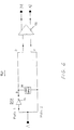
- FIG. 2 shows a differential output structure 30 according to a first embodiment of the invention.
- Output structure 30 includes paths 1 and 2 .
- Path 1 is formed by a series connection of driving elements, such as inverters 12 , 16 and 18 .
- Path 2 is also formed by a series connection of driving elements, such as inverters 26 and 28 .
- Output structure 30 also includes sync circuits 34 and 36 , which dynamically couples the two paths between input A and point C, and between points D and E, respectively.
- Path 1 and path 2 are dynamically coupled because the energy in path 2 is used to aid in the switching of path 1 . This energy transfer occurs when the input to both paths changes logic states (i.e., ground to Vdd or Vdd to ground).
- Output structure 30 further includes an output driver 32 , which is coupled between the outputs of the two paths.
- Driver 32 is a standard differential output driver that may represent any differential output standards (e.g., LVDS, PECL, SSTL, SLVS).
- input A travels along the two paths and is converted to a non-inverted signal M and an inverted signal N.
- path 1 is slower than path 2 due to an additional inverter.
- Sync circuits 34 and 36 provide synchronization functions to the two paths so that signals traveling on path 1 and path 2 arrive at the inputs of driver 32 at substantially the same time.
- Sync circuits 34 and 36 may be implemented, for example, to slow down the two paths by predetermined factors to achieve synchronizations, which is illustrated below in connection with FIG. 3.
- FIG. 3A shows a differential output structure 40 , which is a specific implementation of output structure 30 in FIG. 2.
- sync circuits are implemented with capacitors 42 and 44 , which dynamically couple the two paths.
- Capacitors 42 and 44 are used to slow down the faster path 2 , as will be described below in detail.
- Wp and Wn are the widths of the PMOS and NMOS transistors respectively.
- Other taper and PMOS to NMOS ratios are also possible.
- capacitors 42 and 44 are sized such that capacitor 44 is a chosen factor times larger than capacitor 42 .
- capacitor 44 is four times larger than capacitor 42 .
- Capacitor 42 which is connected between point C and input A, slows down path 2 by a factor of 4, while slowing down path 1 by a factor of 1 since point C is charged at a speed four times faster than at input A. This is because inverter 16 in path 1 has four times the current drive capability to drive capacitor 42 as compared that from input A on path 2 , i.e., there are four times current flowing at point C than at input A. By charging the capacitor 42 faster, it causes signals to move faster. Capacitor 42 also speeds up the logic transition at point C because is dynamically coupled to point A.
- Capacitor 44 functions in a similar manner as capacitor 42 .
- the larger value of capacitor 44 is necessary for the larger sizes of inverters 18 and 26 , which have larger current driving capabilities.
- path 1 may be a 100 ps slower than path 2 without the sync circuit. So the number of delays will slow path 2 and speed up path 1 until they are equal. If path 1 becomes faster than path 2 , then path 1 will be dynamically coupled to path 2 causing these to paths to stay aligned.
- the number of inverters in path 1 and path 2 are usually determined by the size of driver 32 . Furthermore, the dynamically coupling of the slower path to the faster path can be done at all points. A good place to put the sync circuit is in the beginning of the inverter chains after the paths have already split. The number of sync circuits needed depends on the amount of skew between path 1 and path 2 .
- FIGS. 3 B- 3 L show other alternative implementations of the sync circuit, all of which are energy transfer elements or circuits.
- FIG. 4 shows a differential output structure 50 according to a second embodiment of the invention.
- differential output structure 50 includes paths 1 and 2 .
- Path 1 is formed by a series connection of driving elements, such as an exclusive OR (XOR) gate 52 , an inverter 56 and an inverter 58 .
- Path 2 is also formed by a series connection of driving elements, such as an exclusive NOR (XNOR) gate 62 , an inverter 66 and an inverter 68 .
- Path 1 is slower than path 2 due to an additional inversion inherent in the CMOS circuit of gate 52 .
- Output structure 50 also includes sync circuits, such as capacitors 72 and 74 , which dynamically couple the two paths. Additionally, output structure 50 includes an output driver 32 , which is coupled to the outputs of the two paths.
- an input A drives both gates 52 and 62 via one of their inputs.
- Gate 52 has its other input coupled to a power supply Vcc, so that it functions as an inverter.
- gate 62 has its other input coupled to a ground Gnd, so that it functions as a buffer. Input signals travel along the two paths and are output as a non-inverted signal P of the input A and as an inverted signal Q of input A.
- capacitors 72 and 74 are also used to slow down the faster path 2 .
- Capacitors 72 and 74 are sized such that capacitor 74 is four times larger than capacitor 72 .
- Capacitor 72 which is connected between point C and point E, slows down path 2 by a factor of 4, while slowing down path 1 by a factor of 1 since point C is charged at a speed four times faster than at point E. This is because gate 56 in path 1 has four times the current drive capability to drive capacitor 72 as compared to gate 62 in path 2 due to their relative physical sizes, i.e., there are four times current flowing at point C than at point E. By charging the capacitor 72 faster, it causes signals to move faster.
- Capacitor 72 also speeds up the logic transition at point C because point C is dynamically coupled to point E.
- Capacitor 74 functions in a similar manner as capacitor 72 . The larger value of capacitor 74 is necessary for the larger sizes of inverters 58 and 66 , which have larger current driving capabilities.
- FIG. 5 shows a differential output structure 80 according to a third embodiment of the invention.
- Output structure 80 is a variation of structure 30 shown in FIG. 2. It differs from structure 30 in that it does not include inverters 18 and 28 and sync circuit 36 .
- Structure 80 operates in a similar manner as structure 30 in FIG. 2.
- structure 80 includes a driver 82 , which requires a smaller current to operate than that in FIG. 2.
- FIG. 6 shows a differential output structure 90 according to a fourth embodiment of the invention.
- Output structure 90 is a variation of structure 80 shown in FIG. 5. It differs from structure 80 in that it does not include inverters 16 and 26 .
- Structure 90 operates in a similar manner as structure 80 in FIG. 5.
- structure 90 includes a driver 92 , which requires an even smaller current to operate than that in FIG. 5.
Landscapes
- Engineering & Computer Science (AREA)
- Physics & Mathematics (AREA)
- Nonlinear Science (AREA)
- Computer Hardware Design (AREA)
- Computing Systems (AREA)
- General Engineering & Computer Science (AREA)
- Mathematical Physics (AREA)
- Power Engineering (AREA)
- Computer Networks & Wireless Communication (AREA)
- Signal Processing (AREA)
- Logic Circuits (AREA)
Abstract
Description
- The invention relates generally to semiconductor integrated circuit (IC) devices and more particularly, it relates to differential output structures with reduced skew for single inputs.
- In the semiconductor IC industry, board manufacturers are challenged with integrating products with different input and output standards, e.g., TTL (Transistor Transistor Logic) to LVDS (Low Voltage Differential Swing), LVTTL (Low Voltage Transistor Transistor Logic) to LVDS, etc. Typically, when a single input standard such as LVTTL is converted to a differential output standard such as LVDS, the two differential outputs are skewed apart from one another by at least one gate delay, as will be illustrated with reference to FIG. 1.
- FIG. 1 shows a conventional
differential output structure 10, in which a single input A is used to generate two differential and complimentary output signals on output M and output N. In FIG. 1, there are threeinverters inverters - Some solutions have been proposed to limit the skew. One solution is to change the ratios of width/length (W/L) of the inverters in
path 1 andpath 2 in order to match skews at point D and point F in FIG. 1. Another solution is to make the sums of the channel lengths and widths of the inverters inpath 1 equal to the sums of the channel lengths and widths inpath 2, respectively, as follows: - L 12 +L 16 +L 18 =L 26 +L 28
- W 12 +W 16 +W 18 =W 26 +W 28
- where L 12, L16, L18, L26 and L28 are the channel lengths of
inverters inverters - However, these proposed solutions suffer from several drawbacks. When an inverter chain is laid out, a good design practice is to characterize the process and determine the ratio of PMOS (p-type metal oxide semiconductor) and NMOS (n-type metal oxide semiconductor), which gives the desired power consumption, speed, duty cycle, propagation time, etc. For most processes, the ratio of PMOS width (Wp) to NMOS width (Wn) is typically between 2 and 3 to 1. By not using a constant Wp to Wn ratio in the proposed solutions described above, it makes matching every differential inverter path a numerical problem. Moreover, the non-ratioed changing of the length for the PMOS and NMOS devices compounds the problem even further since different lengths and widths add additional processing variations.
- Therefore, there is a need for an improved differential output structure with reduced skew, while introducing less process variations.
- The invention provides an improved differential output structure with minimal skew and introduces less process variations.
- According to one embodiment of the invention, a differential output structure is provided and comprises an input line, an output driver and a sync circuit. The input line includes first and second paths. The first path has an input end for receiving input signals. The first path also has an output end and includes at least one driving element. The second path has an input end operably coupled to the input end of the first path for receiving the input signals. The second path also has an output end. The output driver is operably coupled to the output ends of the first and second paths and is configured to provide differential outputs. The sync circuit is operably coupled between the first and second paths and is configured to synchronize the speed of signals traveling on the two paths.
- Other objects and attainments together with a fuller understanding of the invention will become apparent and appreciated by referring to the following description and claims taken in conjunction with the accompanying drawings.
- The invention is explained in further detail, and by way of example, with reference to the accompanying drawings wherein:
- FIG. 1 shows a conventional differential output structure;
- FIG. 2 shows a differential output structure according to a first embodiment of the invention;
- FIG. 3A shows a specific implementation of the differential output structure in FIG. 2;
- FIGS. 3B-3L show other alternative implementations of the sync circuit;
- FIG. 4 shows a differential output structure according to a second embodiment of the invention;
- FIG. 5 shows a differential output structure according to a third embodiment of the invention;
- FIG. 6 shows a differential output structure according to a fourth embodiment of the invention; and
- FIG. 7 illustrates an alternative embodiment of the invention which includes more than two paths.
- Throughout the drawings, the same reference numerals indicate similar or corresponding features or functions.
- FIG. 2 shows a
differential output structure 30 according to a first embodiment of the invention.Output structure 30 includespaths Path 1 is formed by a series connection of driving elements, such asinverters Path 2 is also formed by a series connection of driving elements, such asinverters Output structure 30 also includessync circuits Path 1 andpath 2 are dynamically coupled because the energy inpath 2 is used to aid in the switching ofpath 1. This energy transfer occurs when the input to both paths changes logic states (i.e., ground to Vdd or Vdd to ground). The transfer of energy slows downpath 2 and speeds uppath 1.Output structure 30 further includes anoutput driver 32, which is coupled between the outputs of the two paths.Driver 32 is a standard differential output driver that may represent any differential output standards (e.g., LVDS, PECL, SSTL, SLVS). In FIG. 2, input A travels along the two paths and is converted to a non-inverted signal M and an inverted signal N. - In FIG. 2,
path 1 is slower thanpath 2 due to an additional inverter.Sync circuits path 1 andpath 2 arrive at the inputs ofdriver 32 at substantially the same time.Sync circuits - FIG. 3A shows a
differential output structure 40, which is a specific implementation ofoutput structure 30 in FIG. 2. In FIG. 3A, sync circuits are implemented withcapacitors 42 and 44, which dynamically couple the two paths.Capacitors 42 and 44 are used to slow down thefaster path 2, as will be described below in detail. - In this embodiment, as in FIG. 2, the following parameters are used, i.e., taper ratio=4, and Wp/Wn=3 for each gate, where Wp and Wn are the widths of the PMOS and NMOS transistors respectively. Other taper and PMOS to NMOS ratios are also possible. Assuming Wn=1 and Ln=Lp=1,
path 1 would be sized as follows: for inverter 12: Wp/Lp=3/1, Wn/Ln=1/1; for inverter 16: 4*(inverter 12), i.e., Wp/Lp=12/1, Wn/Ln=4/1; and for inverter 18: 16*(inverter 12), i.e., Wp/Lp=48/1, Wn/Ln =16/1. Similarly,path 2 would be sized as follows: for inverter 26: 4*(inverter 12), i.e., Wp/Lp =12/1, Wn/Ln=4/1; and for inverter 28: 16*(inverter 12), i.e., Wp/Lp=48/1, Wn/Ln=16/1. - In FIG. 3A,
capacitors 42 and 44 are sized such thatcapacitor 44 is a chosen factor times larger than capacitor 42. In this example,capacitor 44 is four times larger than capacitor 42. Capacitor 42, which is connected between point C and input A, slows downpath 2 by a factor of 4, while slowing downpath 1 by a factor of 1 since point C is charged at a speed four times faster than at input A. This is becauseinverter 16 inpath 1 has four times the current drive capability to drive capacitor 42 as compared that from input A onpath 2, i.e., there are four times current flowing at point C than at input A. By charging the capacitor 42 faster, it causes signals to move faster. Capacitor 42 also speeds up the logic transition at point C because is dynamically coupled to point A. -
Capacitor 44 functions in a similar manner as capacitor 42. The larger value ofcapacitor 44 is necessary for the larger sizes ofinverters - The capacitors in FIG. 3
align path 1 withpath 2. For example,path 1 may be a 100 ps slower thanpath 2 without the sync circuit. So the number of delays will slowpath 2 and speed uppath 1 until they are equal. Ifpath 1 becomes faster thanpath 2, thenpath 1 will be dynamically coupled topath 2 causing these to paths to stay aligned. - The number of inverters in
path 1 andpath 2 are usually determined by the size ofdriver 32. Furthermore, the dynamically coupling of the slower path to the faster path can be done at all points. A good place to put the sync circuit is in the beginning of the inverter chains after the paths have already split. The number of sync circuits needed depends on the amount of skew betweenpath 1 andpath 2. - FIGS. 3B-3L show other alternative implementations of the sync circuit, all of which are energy transfer elements or circuits.
- FIG. 4 shows a
differential output structure 50 according to a second embodiment of the invention. In FIG. 4,differential output structure 50 includespaths Path 1 is formed by a series connection of driving elements, such as an exclusive OR (XOR)gate 52, aninverter 56 and aninverter 58.Path 2 is also formed by a series connection of driving elements, such as an exclusive NOR (XNOR)gate 62, aninverter 66 and aninverter 68.Path 1 is slower thanpath 2 due to an additional inversion inherent in the CMOS circuit ofgate 52.Output structure 50 also includes sync circuits, such ascapacitors output structure 50 includes anoutput driver 32, which is coupled to the outputs of the two paths. - In this embodiment, similar parameters as in FIG. 3A are used, i.e., taper ratio=4, and Wp/Wn=3 for each gate, where Wp and Wn are the widths of the PMOS and NMOS transistors respectively. Again other taper and PMOS to NMOS ratios are possible. Assuming Wn=1 and Ln=Lp=1,
path 1 would be sized as follows: for gate 52: Wp/Lp=3/1, Wn/Ln=1/1; for inverter 56: 4*(gate 52), i.e., Wp/Lp=12/1, Wn/Ln=4/1; and for inverter 58: 16*(gate 52), i.e., Wp/Lp=48/1, Wn/Ln=16/1. Similarly,path 2 would be sized as follows: for gate 62: Wp/Lp=3/1, Wn/Ln=1/1; for inverter 66: 4*(gate 62), i.e., Wp/Lp=12/1, Wn/Ln=4/1; and for inverter 68: 16*(gate 62), i.e., Wp/Lp=48/1, Wn/Ln=16/1. - In FIG. 4, an input A drives both
gates Gate 52 has its other input coupled to a power supply Vcc, so that it functions as an inverter. On the other hand,gate 62 has its other input coupled to a ground Gnd, so that it functions as a buffer. Input signals travel along the two paths and are output as a non-inverted signal P of the input A and as an inverted signal Q of input A. - In this embodiment, as in FIG. 3A,
capacitors faster path 2.Capacitors capacitor 74 is four times larger thancapacitor 72.Capacitor 72, which is connected between point C and point E, slows downpath 2 by a factor of 4, while slowing downpath 1 by a factor of 1 since point C is charged at a speed four times faster than at point E. This is becausegate 56 inpath 1 has four times the current drive capability to drivecapacitor 72 as compared togate 62 inpath 2 due to their relative physical sizes, i.e., there are four times current flowing at point C than at point E. By charging thecapacitor 72 faster, it causes signals to move faster.Capacitor 72 also speeds up the logic transition at point C because point C is dynamically coupled to pointE. Capacitor 74 functions in a similar manner ascapacitor 72. The larger value ofcapacitor 74 is necessary for the larger sizes ofinverters - FIG. 5 shows a
differential output structure 80 according to a third embodiment of the invention.Output structure 80 is a variation ofstructure 30 shown in FIG. 2. It differs fromstructure 30 in that it does not includeinverters sync circuit 36.Structure 80 operates in a similar manner asstructure 30 in FIG. 2. In this embodiment,structure 80 includes adriver 82, which requires a smaller current to operate than that in FIG. 2. - FIG. 6 shows a
differential output structure 90 according to a fourth embodiment of the invention.Output structure 90 is a variation ofstructure 80 shown in FIG. 5. It differs fromstructure 80 in that it does not includeinverters Structure 90 operates in a similar manner asstructure 80 in FIG. 5. In this embodiment,structure 90 includes adriver 92, which requires an even smaller current to operate than that in FIG. 5. - It should be noted that there can be more than two paths as long as the gate elements, e.g., inverters, are differential, such as illustrated in FIG. 7.
- While the invention has been described in conjunction with specific embodiments, it is evident that many alternatives, modifications and variations will be apparent to those skilled in the art in light of the foregoing description. Accordingly, it is intended to embrace all such alternatives, modifications and variations as fall within the spirit and scope of the appended claims.
Claims (20)
Priority Applications (4)
| Application Number | Priority Date | Filing Date | Title |
|---|---|---|---|
| US10/125,963 US6700420B2 (en) | 2002-04-18 | 2002-04-18 | Differential output structure with reduced skew for a single input |
| CNB031360092A CN100521538C (en) | 2002-04-18 | 2003-04-15 | Differential output structure with decreased bias under single input |
| TW092108659A TW200408192A (en) | 2002-04-18 | 2003-04-15 | Differential output structure with reduced skew for a single input |
| US10/678,937 US6836163B2 (en) | 2002-04-18 | 2003-10-03 | Differential output structure with reduced skew for a single input |
Applications Claiming Priority (1)
| Application Number | Priority Date | Filing Date | Title |
|---|---|---|---|
| US10/125,963 US6700420B2 (en) | 2002-04-18 | 2002-04-18 | Differential output structure with reduced skew for a single input |
Related Child Applications (1)
| Application Number | Title | Priority Date | Filing Date |
|---|---|---|---|
| US10/678,937 Continuation US6836163B2 (en) | 2002-04-18 | 2003-10-03 | Differential output structure with reduced skew for a single input |
Publications (2)
| Publication Number | Publication Date |
|---|---|
| US20030197539A1 true US20030197539A1 (en) | 2003-10-23 |
| US6700420B2 US6700420B2 (en) | 2004-03-02 |
Family
ID=29214894
Family Applications (2)
| Application Number | Title | Priority Date | Filing Date |
|---|---|---|---|
| US10/125,963 Expired - Lifetime US6700420B2 (en) | 2002-04-18 | 2002-04-18 | Differential output structure with reduced skew for a single input |
| US10/678,937 Expired - Lifetime US6836163B2 (en) | 2002-04-18 | 2003-10-03 | Differential output structure with reduced skew for a single input |
Family Applications After (1)
| Application Number | Title | Priority Date | Filing Date |
|---|---|---|---|
| US10/678,937 Expired - Lifetime US6836163B2 (en) | 2002-04-18 | 2003-10-03 | Differential output structure with reduced skew for a single input |
Country Status (3)
| Country | Link |
|---|---|
| US (2) | US6700420B2 (en) |
| CN (1) | CN100521538C (en) |
| TW (1) | TW200408192A (en) |
Families Citing this family (18)
| Publication number | Priority date | Publication date | Assignee | Title |
|---|---|---|---|---|
| DE10255642B4 (en) * | 2002-11-28 | 2006-07-13 | Infineon Technologies Ag | Method and device for outputting a digital signal |
| US20060044016A1 (en) * | 2004-08-24 | 2006-03-02 | Gasper Martin J Jr | Integrated circuit with signal skew adjusting cell selected from cell library |
| US7332818B2 (en) * | 2005-05-12 | 2008-02-19 | Endicott Interconnect Technologies, Inc. | Multi-chip electronic package with reduced line skew and circuitized substrate for use therein |
| US7368950B2 (en) * | 2005-11-16 | 2008-05-06 | Montage Technology Group Limited | High speed transceiver with low power consumption |
| TWI283966B (en) * | 2005-12-21 | 2007-07-11 | Univ Nat Central | Low-voltage, high-frequency frequency divider having dual-mode operation |
| US7800184B2 (en) * | 2006-01-09 | 2010-09-21 | International Business Machines Corporation | Integrated circuit structures with silicon germanium film incorporated as local interconnect and/or contact |
| US8230285B2 (en) * | 2006-02-17 | 2012-07-24 | Jds Uniphase Corporation | Protocol analyzer for consumer electronics |
| US8127190B2 (en) * | 2006-02-17 | 2012-02-28 | Lanning Eric J | Sampling a device bus |
| US7443217B2 (en) * | 2006-03-07 | 2008-10-28 | Texas Instruments Incorporated | Circuit and method to balance delays through true and complement phases of differential and complementary drivers |
| US7477086B1 (en) | 2006-09-22 | 2009-01-13 | Altera Corporation | Low-skew digital lever shifter for I/O |
| US7463080B2 (en) * | 2007-04-06 | 2008-12-09 | Maxim Integrated Products, Inc. | Methods and systems for converting a single-ended signal to a differential signal |
| US8242823B2 (en) * | 2009-04-27 | 2012-08-14 | Oracle America, Inc. | Delay chain initialization |
| US8179165B2 (en) * | 2009-04-27 | 2012-05-15 | Oracle America, Inc. | Precision sampling circuit |
| US8283960B2 (en) * | 2009-04-27 | 2012-10-09 | Oracle America, Inc. | Minimal bubble voltage regulator |
| US8198931B2 (en) * | 2009-04-27 | 2012-06-12 | Oracle America, Inc. | Fine grain timing |
| WO2011142148A1 (en) * | 2010-05-14 | 2011-11-17 | シャープ株式会社 | Level shift circuit and display device provided with the same |
| KR101998173B1 (en) * | 2012-12-24 | 2019-10-17 | 에스케이하이닉스 주식회사 | Phase splitter |
| US20250300645A1 (en) * | 2024-03-21 | 2025-09-25 | Taiwan Semiconductor Manufacturing Company, Ltd. | System, Device, and Method for Transforming a Single-Ended Input Signal Into Differential Output Signals |
Family Cites Families (5)
| Publication number | Priority date | Publication date | Assignee | Title |
|---|---|---|---|---|
| US5375148A (en) * | 1993-03-01 | 1994-12-20 | Motorola, Inc. | VCO bias generator in a phase lock loop |
| US5909134A (en) * | 1995-12-18 | 1999-06-01 | Lg Semicon Co., Ltd. | Clock generator for generating complementary clock signals with minimal time differences |
| US6246278B1 (en) * | 1995-12-22 | 2001-06-12 | Lsi Logic Corporation | High speed single phase to dual phase clock divider |
| US6107847A (en) * | 1997-12-30 | 2000-08-22 | Rambus Inc. | Zero power reset circuit for low voltage CMOS circuits |
| US6420920B1 (en) * | 2000-08-28 | 2002-07-16 | Micron Technology, Inc. | Method and apparatus for phase-splitting a clock signal |
-
2002
- 2002-04-18 US US10/125,963 patent/US6700420B2/en not_active Expired - Lifetime
-
2003
- 2003-04-15 TW TW092108659A patent/TW200408192A/en unknown
- 2003-04-15 CN CNB031360092A patent/CN100521538C/en not_active Expired - Fee Related
- 2003-10-03 US US10/678,937 patent/US6836163B2/en not_active Expired - Lifetime
Also Published As
| Publication number | Publication date |
|---|---|
| US20040066216A1 (en) | 2004-04-08 |
| CN1452318A (en) | 2003-10-29 |
| US6700420B2 (en) | 2004-03-02 |
| US6836163B2 (en) | 2004-12-28 |
| TW200408192A (en) | 2004-05-16 |
| CN100521538C (en) | 2009-07-29 |
Similar Documents
| Publication | Publication Date | Title |
|---|---|---|
| US6700420B2 (en) | Differential output structure with reduced skew for a single input | |
| US6724218B2 (en) | Digital logic devices with extremely skewed trip points and reset circuitry for rapidly propagating signal edges | |
| US5926050A (en) | Separate set/reset paths for time critical signals | |
| US8334709B2 (en) | Level shifter | |
| EP1166443B1 (en) | Single rail domino logic for four-phase clocking scheme | |
| US7355446B2 (en) | Voltage conversion circuit with stable transition delay characteristic | |
| US6617881B2 (en) | Semiconductor integrated circuit | |
| US6661274B1 (en) | Level converter circuit | |
| US6734705B2 (en) | Technique for improving propagation delay of low voltage to high voltage level shifters | |
| KR19980071674A (en) | Complementary Metal Oxide Semiconductor Circuit | |
| US20020186050A1 (en) | Logic circuit for true and complement signal generator | |
| US6373292B1 (en) | Low voltage differential logic | |
| US6429687B1 (en) | Semiconductor integrated circuit device | |
| KR100305710B1 (en) | Sense amplifier-based CMOS flip-flop with enhanced output transition speed | |
| US20050207504A1 (en) | Signal transmission circuit | |
| KR102674627B1 (en) | Level shifter | |
| JP2000101417A (en) | Inverter circuit and inverter buffer | |
| KR19980083562A (en) | Dynamic input buffer |
Legal Events
| Date | Code | Title | Description |
|---|---|---|---|
| AS | Assignment |
Owner name: KONINKLIJKE PHILIPS ELECTRONICS N.V., NETHERLANDS Free format text: ASSIGNMENT OF ASSIGNORS INTEREST;ASSIGNOR:SPEHAR, JAMES R.;REEL/FRAME:012845/0693 Effective date: 20020417 |
|
| STCF | Information on status: patent grant |
Free format text: PATENTED CASE |
|
| AS | Assignment |
Owner name: NXP B.V., NETHERLANDS Free format text: ASSIGNMENT OF ASSIGNORS INTEREST;ASSIGNOR:KONINKLIJKE PHILIPS ELECTRONICS N.V.;REEL/FRAME:018635/0787 Effective date: 20061117 |
|
| FPAY | Fee payment |
Year of fee payment: 4 |
|
| FPAY | Fee payment |
Year of fee payment: 8 |
|
| AS | Assignment |
Owner name: PARTNERS FOR CORPORATE RESEARCH INTERNATIONAL, CAY Free format text: ASSIGNMENT OF ASSIGNORS INTEREST;ASSIGNOR:NXP B. V.;REEL/FRAME:031334/0449 Effective date: 20120907 |
|
| AS | Assignment |
Owner name: FUTURE LINK SYSTEMS, CALIFORNIA Free format text: ASSIGNMENT OF ASSIGNORS INTEREST;ASSIGNOR:PARTNERS FOR CORPORATE RESEARCH INTERNATIONAL;REEL/FRAME:032399/0965 Effective date: 20130808 |
|
| FPAY | Fee payment |
Year of fee payment: 12 |